EP1482524A1 - Laminate type electronic component - Google Patents
Laminate type electronic component Download PDFInfo
- Publication number
- EP1482524A1 EP1482524A1 EP03743633A EP03743633A EP1482524A1 EP 1482524 A1 EP1482524 A1 EP 1482524A1 EP 03743633 A EP03743633 A EP 03743633A EP 03743633 A EP03743633 A EP 03743633A EP 1482524 A1 EP1482524 A1 EP 1482524A1
- Authority
- EP
- European Patent Office
- Prior art keywords
- electronic component
- particle
- type electronic
- dielectric
- resin
- Prior art date
- Legal status (The legal status is an assumption and is not a legal conclusion. Google has not performed a legal analysis and makes no representation as to the accuracy of the status listed.)
- Granted
Links
Images

Classifications
-
- H—ELECTRICITY
- H01—ELECTRIC ELEMENTS
- H01G—CAPACITORS; CAPACITORS, RECTIFIERS, DETECTORS, SWITCHING DEVICES, LIGHT-SENSITIVE OR TEMPERATURE-SENSITIVE DEVICES OF THE ELECTROLYTIC TYPE
- H01G4/00—Fixed capacitors; Processes of their manufacture
- H01G4/002—Details
- H01G4/228—Terminals
- H01G4/232—Terminals electrically connecting two or more layers of a stacked or rolled capacitor
- H01G4/2325—Terminals electrically connecting two or more layers of a stacked or rolled capacitor characterised by the material of the terminals
Definitions
- the present invention relates to a laminate type electronic component and, more specifically, to a laminate type electronic component such as a laminated ceramic capacitor.
- Switching power supplies and DC/DC converters have currently been employed in many of power supplies of electronic devices.
- a capacitor used in these power supplies is a power supply bypass capacitor.
- an aluminum electrolytic capacitor or tantalum electrolytic capacitor having a large capacity or a laminated ceramic capacitor having a low capacity has been used according to circuit parameters such as its power capacity and switching frequency and a smoothing coil employed.
- the electrolytic capacitors mentioned above have excellent advantages in that they can easily attain a large capacity as a power supply bypass (smoothing) capacitor, they are problematic in that they are large in size; they are poor in low-temperature characteristics; they arouse a fear of short-circuiting; their internal impedance is relatively high, so that their dielectric dissipation factor (tan ⁇ ) due to equivalent series resistance (hereinafter referred to as "ESR") is high, whereby loss occurs steadily, which generates heat; they fail to attain sufficient frequency characteristics, so that their smoothness is insufficient; etc.
- ESR equivalent series resistance
- ripple noise In power supply bypass capacitors, it is important to reduce ripple noise in order to attain a sufficient smoothing action.
- the ripple noise can be suppressed if the ESR of the capacitor is reduced.
- capacitors having a low ESR be used in power supply bypass circuits, whereby proposals to use laminated ceramic capacitors having a low ESR in power supply circuits have been under study.
- the ESR of the smoothing circuit greatly influences phase characteristics of a feedback loop in secondary circuits such as a DC/DC converter having a feedback circuit to become a power supply and a switching power supply, in particular, the ESR may become extremely low, whereby it has been impossible to attain sufficient reliability.
- the secondary smoothing circuit is equivalently constituted by L and C components alone, so that only ⁇ 90 degrees and 0 degree exist as phase components existing in the circuit, and phases have no room, whereby oscillations are easy to occur. This oscillation phenomenon has also occurred when load fluctuates in a power supply circuit using a three-terminal regulator.
- Japanese Patent Application Laid-Open No. HEI 8-45784 proposes an electronic component in which an end part of a laminated ceramic capacitor is turned into a semiconductor by using a carbide and a reducing agent.
- Japanese Patent Application Laid-Open No. SHO 59-225509 discloses one in which a resistive paste such as ruthenium oxide is laminated on a laminated ceramic capacitor, and they are baked at the same time, so as to yield a resistive element.
- Japanese Patent Publication No. 2578264 proposes a CR composite component in which a metal oxide film is provided on a surface of an external electrode, in order to attain a desirable ESR.
- the conductive resin contains spherical or scaly particles made of a metal such as silver.
- the ESR of this type of smoothing capacitor is relatively low in general, i.e., 10 m ⁇ or less. Therefore, in order for the ESR of the external electrode to rise to at least 40 m ⁇ , which is said to be able to sufficiently prevent the above-mentioned oscillation phenomenon from occurring, the content of the conductive material is required to be as small as possible, for which studies have been under way.
- the laminated ceramic capacitor disclosed in Japanese Patent Application Laid-Open No. SHO 59-225509 has a configuration having the above-mentioned resistive element formed by using a resistive paste such as ruthenium oxide, when an external electrode is further provided, the equivalent circuit becomes a parallel circuit of C/R or (LC)/R and fails to yield a series circuit. Also, in order for this laminated ceramic capacitor to yield a series circuit, the external electrode requires a complicated form and a complicated manufacturing step, and the manufacturing efficiency becomes low, whereby there is no configuration capable of yielding a sufficient mass productivity.
- a resistive paste such as ruthenium oxide
- a metal oxide film is formed by heating a terminal electrode comprising nickel as a constituent material, and the thickness of the metal oxide film is adjusted by barrel polishing, whereby a desirable resistance value is obtained (see Examples). Therefore, the CR composite component is also hard to yield a desirable resistance value, the adjustment of the resistance value is troublesome, the manufacturing efficiency is low, and there is no configuration capable of yielding a sufficient mass productivity.
- the inventors have found that the above-mentioned object can be achieved in a laminate type electronic component having an external electrode comprising a conductive resin as a constituent material, when the value of ESR is adjusted to 40 to 150 m ⁇ while the fluctuation (standard deviation) of the value of ESR obtained at the time of operation is adjusted to 10 m ⁇ or less.
- the inventors have found that the value of ESR and its fluctuation (standard deviation) can be adjusted within the ranges mentioned above easily and reliably if a particle satisfying specific geometric conditions concerning its form is contained as a conductive particle contained in a conductive resin and the content of the particle is within a particular range when forming an external electrode comprising the conductive particle as a constituent material, thereby achieving the present invention.
- the present invention provides a laminate type electronic component comprising at least:
- the present invention can easily and reliably yield a laminate type electronic component having an ESR value of 40 to 150 m ⁇ with a fluctuation (standard deviation) of 10 m ⁇ or less in the ESR value at the time of operation.
- the laminate type electronic component satisfying these two electric characteristic conditions at the same time has a DC resistance or impedance within a range usable in a smoothing circuit or the like of a switching power supply circuit having various circuit constants.
- the laminate type electronic component satisfying the above-mentioned two electric characteristic conditions can easily and reliably yield a laminate type electronic component having an excellent reliability, which can sufficiently prevent the oscillation phenomenon from occurring and attain a sufficient smoothing action even when employed in a power supply bypass circuit.
- the resin electrode layers of the external electrodes are mainly composed of the conductive particle and the thermosetting resin, they can be made easily with a favorable reproducibility so as to satisfy the above-mentioned two electric characteristic conditions. Therefore, the laminate type electronic component in accordance with the present invention is excellent in mass productivity.
- the ESR value When the ESR value is less than 40 m ⁇ here, the oscillation phenomenon occurs easily. When the ESR value exceeds 150 m ⁇ , by contrast, the conductivity of the external electrodes (first and second external electrodes) drops remarkably, and frequency characteristics also deteriorate remarkably. If one having an ESR value exceeding 150 m ⁇ is employed in a power supply circuit, the current loss is so large that desirable power supply voltage and current cannot be obtained.
- the ESR value is 40 m ⁇ or more, the electronic component can sufficiently prevent the oscillation phenomenon from occurring even when employed in a power supply bypass circuit.
- the ESR value (40 m ⁇ ) to become a threshold of whether the oscillation phenomenon can sufficiently be prevented from occurring or not is a value calculated in view of various circuit constants (electrostatic capacity, inductance, and impedance) of substantially all the kinds of switching power supplies.
- the inventors have also found that, when the fluctuation (standard deviation) of the ESR value exceeds 10 m ⁇ , outputs of the power supply voltage and power supply current cannot be controlled, whereby the above-mentioned effects of the present invention cannot be obtained. From the viewpoint of controlling the output of power supply current more reliably, it will be preferred if the fluctuation (standard deviation) of the ESR value is 8 m ⁇ or less.
- the conductive particle content in the conductive resin constituting the resin electrode layer is less than 70 mass% in the present invention, the electric resistance of the first and second external electrodes increases so much that the electronic component cannot attain a conductivity sufficient for functioning as an electrode.
- the conductivity of the first and second external electrodes increases so much that the ESR value becomes less than 40 m ⁇ . From the foregoing viewpoint, the conductive particle content in the conductive resin constituting the resin electrode layer is 70 to 75 mass%.
- geometric conditions concerning the form of the acicular particle to become a main ingredient of the conductive particle are as follows. Namely, it has an average longitudinal length of 30 to 70 ⁇ m and an aspect ratio of 1.5 to 3.3.
- the laminate type electronic component satisfying the above-mentioned two electric characteristic conditions concerning the ESR can be constructed easily.
- average longitudinal length refers to an average value of major axes of acicular particles having an anisotropic shape and, more specifically, to an arithmetic average value of major axes of 30 acicular particles randomly sampled from those disposed at a cross section observed by SEM in an external electrode (first or second external electrode) to become a measurement sample.
- average latitudinal length refers to an arithmetic average value of major axes of 30 acicular particles randomly sampled from those disposed at a cross section observed by SEM in an external electrode (first or second external electrode) to become a measurement sample.
- the ESR value decreases, or the fluctuation (standard deviation) of ESR value increases, whereby the above-mentioned effects of the present invention cannot be obtained.
- the average longitudinal length of acicular particles exceeds 70 ⁇ m, the fluctuation (standard deviation) of ESR value increases, so that the above-mentioned effects of the present invention cannot be obtained.
- the “aspect ratio” refers to [(average longitudinal length)/(average latitudinal length)].
- the aspect ratio When the aspect ratio is less than 1.5, the ESR value becomes lower, so that the above-mentioned effects of the present invention cannot be obtained.
- the aspect ratio exceeds 3.3, the fluctuation (standard deviation) of ESR value becomes greater, so that the above-mentioned effects of the present invention cannot be obtained.
- the content of the acicular particle, which is a main ingredient of the conductive particle, in the conductive particle is at least 40 mass%, preferably 40 to 75 mass%.
- the acicular particle content in the conductive particle is less than 40 mass%, the electric resistance of the first and second external electrodes increases so much that they cannot obtain a conductivity sufficient for functioning as an electrode of the electronic component, whereby the above-mentioned effects of the present invention cannot be obtained.
- the conductivity of the first and second external electrodes increases so much that the ESR value is more likely to become less than 40 m ⁇ .
- the acicular particle is a particle (Ag filler) comprising Ag.
- the inventors have found that the above-mentioned effects of the present invention can be obtained more reliably when this particle is used.
- the conductive particle further contains a spherical particle having an average particle size of 3 to 20 ⁇ m therein, and has an acicular particle content of 40 to 75 mass% and a spherical particle content of 15 to 35 mass% therein.
- the inventors have found that the above-mentioned effects of the present invention can be obtained more reliably when the three numerical range conditions mentioned above are satisfied at the same time in the case where the spherical particle is used together with the acicular particle.
- the contact resistance between spherical particles increases, so that the electric resistance of the first and second external electrodes (electric resistance of each of the resin electrode layers in the first and second external electrodes) becomes too high, whereby they are less likely to attain a conductivity sufficient for functioning as an electrode of the electronic component.
- the average particle size of the spherical particle is less than 3 ⁇ m, the viscosity of a paste containing the spherical particle for forming each resin electrode layer increases, so that electrodes are harder to form.
- spherical particle refers to a particle having an average particle size of 3 to 20 ⁇ m and an aspect ratio of 1.0 to 1.2.
- the "average particle size” of the spherical particle refers to an arithmetic average value of respective maximum particle sizes of 30 spherical particles randomly sampled from those disposed at a cross section observed by SEM in an external electrode (first or second external electrode) containing spherical particles to become a measurement sample.
- the electric resistance of the first and second external electrodes increases so much that they are less likely to attain a conductivity sufficient for functioning as an electrode of the electronic component.
- the conductivity of the first and second external electrodes increases so much that the ESR value is more likely to become less than 40 m ⁇ .
- the acicular particle content in the conductive particle is less than 40 mass% when the spherical particle is used together with the acicular particle, the electric resistance of the first and second external electrodes (electric resistance of each of the resin electrode layers in the first and second external electrodes) increases so much that the they are less likely to attain a conductivity sufficient for functioning as an electrode of the electronic component.
- the conductivity of the first and second external electrodes increases so much that the ESR value is more likely to become less than 40 m ⁇ .
- the spherical particle is a particle (Ag filler) comprising Ag.
- the inventors have found that the above-mentioned effects of the present invention can be obtained more reliably when this particle is used.
- each of the first and second external electrodes is further provided with a metal electrode layer comprising a metal disposed between the resin electrode layer and dielectric part.
- the electric contact state between the resin electrode layer and the internal electrode in the dielectric part can be made better than that in the case where the resin electrode layer is directly formed on the surface of the dielectric part, whereby the electric contact resistance between the resin electrode layer and the dielectric part occurring when the resin electrode layer is directly formed on the surface of the dielectric powder can sufficiently be lowered in an easy and reliable manner.
- the resin electrode layer can physically be secured to the dielectric part more firmly.
- the metal electrode layer is formed by sintering a paste mainly composed of any of metals of Cu, Ag, Pd, Ni, and Ag-Pd alloy, from the viewpoint of sufficiently lowering the above-mentioned electric resistance and from the viewpoint of manufacturing efficiency.
- a Ni plating layer formed from Ni by plating is further disposed on an outer surface of the resin electrode layer.
- electrolytic plating can be employed as the plating in this case.
- an Sn plating layer formed from Sn by plating is further disposed on an outer surface of the Ni plating layer.
- Electrolytic plating can be employed as the plating in this case as well.
- the at least two internal electrodes are disposed in the dielectric part such that one of the two internal electrodes adjacent each other by way of the dielectric layer is electrically connected to the first external electrode whereas the other is electrically connected to the second external electrode.
- This can yield a laminate type electronic component which is easy to be made compact and has an excellent charging/discharging efficiency.
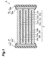
- Fig. 1 is a schematic sectional view showing the basic configuration of a preferred embodiment (laminated ceramic capacitor) of the laminate type electronic component in accordance with the present invention.
- Fig. 2 is a partly enlarged sectional view schematically showing the inner structure of the first and second external electrodes shown in Fig. 1.
- the laminated ceramic capacitor 1 shown in Fig. 1 comprises a dielectric part 2 containing a dielectric as a constituent material, and a pair of a first external electrode 31 and a second external electrode 32, each disposed in close contact with the dielectric part 2, opposing each other by way of the dielectric part 2.
- the dielectric part 2 comprises at least two internal electrodes (electrode plates 23a to 23e which will be explained later) each electrically connected to one of the first external electrode 31 and second external electrode 32, and at least one dielectric layer made of the dielectric and disposed one by one between electrodes adjacent each other in the at least two internal electrodes.
- At least one of the at least two internal electrodes is electrically connected to the first external electrode, and at least one of the at least two internal electrodes is electrically connected to the second external electrode.
- the dielectric part 2 made of a dielectric is constituted by six dielectric layers 21a to 21f and five rectangular electrode plates 23a to 23e.
- the dielectric layers 21a to 21f are configured such that the dielectric layer 21a is disposed on one bottom face of the dielectric part 2 having a substantially rectangular parallelepiped shape, and the dielectric layers 21b to 21f are successively disposed thereon.
- the electrode plates 23a to 23e to become the internal electrodes are disposed between the dielectric layers 21b and 21c, between the dielectric layers 21c and 21d, between the dielectric layers 21d and 21e, and between the dielectric layers 21e and 21f, respectively, while in close contact with their corresponding dielectric layers holding them.
- the electrode plates 23a, 23c, and 23e are electrically connected to the first external electrode 31, whereas the electrode plates 23b and 23d are connected to the second external electrode 32.
- at least two internal electrodes are disposed in the second dielectric part 2 such that one of the two internal electrodes adjacent each other by way of a dielectric layer is electrically connected to the first external electrode 31, whereas the other is electrically connected to the second external electrode 32.
- This laminated ceramic capacitor 1 functions as a passive device which generates an electrostatic capacity component between each pair of internal electrodes.
- each of the first external electrode 31 and second external electrode 32 has the following configuration.
- the first external electrode 31 and second external electrode 32 comprise resin electrode layers 31a and 32a, each made of a conductive resin mainly composed of a thermosetting resin 6 and a conductive particle 7; a metal electrode layer 31b disposed between the resin electrode layer 31a and the dielectric part 2; and a metal electrode layer 32b disposed between the resin electrode layer 32a and the dielectric part 2.
- the resin electrode layers 31a and 32a are connected to the dielectric part 2 by way of the metal electrode layers 31b and 32b, respectively, electric contact states of the resin electrode layers 31a and 32a with the internal electrodes (resin electrode layers 23a to 23e) within the dielectric part 2 can be made better than those in the case where the resin electrode layers 31a and 32a are directly formed on the surface of the dielectric part 2, whereby the electric contact resistance between the dielectric part 2 and the resin electrode layers 31a and 32a occurring when the resin electrode layers 31a and 32a are directly formed on the surface of the dielectric part 2 can sufficiently be lowered in an easy and reliable manner.
- the resin electrode layers 31a and 32a can physically be secured to the dielectric part 2 more firmly by way of the metal electrode layers 31b, 32b, respectively.
- the metal electrode layers 31b and 32b are preferably formed by sintering a paste mainly composed of any of metals of Cu, Ag, Pd, Ni, and Ag-Pd alloy, more preferably formed by sintering a paste mainly composed of Cu.
- the conductive particle content in the conductive resin in the resin electrode layers 31a and 32a is 70 to 75 mass% as mentioned above.
- the conductive particle 7 contains, as main ingredients, acicular particles 71 having an average longitudinal length of 30 to 70 ⁇ m and an aspect ratio of 1.5 to 3.3 and spherical particles 72 having an average particle size of 3 to 20 ⁇ m.
- the content of the acicular particles 71 in the conductive particle is 40 to 75 mass%, while the content of the spherical particles 72 in the conductive particle is 15 to 35 mass%.
- both the acicular particles 71 and spherical particles 72 are particles made of Ag.
- thermosetting resin 6 examples include epoxy resins, phenol resins, etc. From the viewpoints of heat resistance and high-frequency characteristics, the epoxy resins are preferred in particular among the thermosetting resins.
- the electrode plates 23a to 23e are not restricted in particular as long as they have an electronic conductivity usable in a laminated ceramic capacitor, whereby those made of the same constituent material as with internal electrodes mounted to known laminated ceramic capacitors can be used.
- those made of the same constituent material as with internal electrodes mounted to known laminated ceramic capacitors can be used.
- Cu, Ni, Ag-Pd alloy, etc. can be used.
- the laminated ceramic capacitor 1 allows the laminated ceramic capacitor 1 to have an ESR value of 40 to 150 m ⁇ with a fluctuation (standard deviation) of 10 m ⁇ or less in the ESR value at the time of operation.
- the laminated ceramic capacitor 1 has a DC resistance or impedance within a range usable in a smoothing circuit or the like of a switching power supply circuit having various circuit constants.
- the laminated ceramic capacitor 1 has such an excellent reliability that it can sufficiently prevent the oscillation phenomenon from occurring and attain a sufficient smoothing action even when used in a power supply bypass circuit.
- the laminated ceramic capacitor 1 can be made by the same thin-film manufacturing technique as with the making of a known laminated ceramic capacitor except that the ingredients contained in the first external electrode 31 and second external electrode 32 and their compositions are adjusted to the conditions mentioned above.
- an Ni plating layer formed from Ni by plating may further be disposed on the outer surfaces of the resin electrode layers 31a and 32a.
- an Sn plating layer formed from Sn by plating may further be disposed on the outer surface of each of the Ni plating layers of the resin electrode layers 31a and 32a.
- protective layers (having a thickness of 50 to 100 ⁇ m, for example) made of the same constituent material as with the dielectric layers 21a and 21f may further be disposed on respective outer surfaces of the dielectric part 2 (respective outer surfaces of the dielectric layers 21a and 21f).
- a paste containing a dielectric material was prepared, and then each dielectric layer was formed from this paste by doctor blading.
- Each internal electrode comprising Ni was formed by preparing a Ni paste mainly composed of Ni and then printing this paste on each dielectric layer by a printing process.
- the dielectric part was heat-treated in the air under a temperature condition of 400° to 600°C, so as to eliminate the binder component contained in the dielectric part.
- the resulting dielectric part was further sintered (baked) in the air under a temperature condition of 1250° to 1360°C.
- the first and second external electrodes were formed on surfaces of the resulting sintered (baked) dielectric part.
- the first and second external electrodes were formed on respective surfaces, parallel to a surface perpendicular to the contact surface of each dielectric layer, opposing each other in the dielectric part having a rectangular parallelepiped shape.
- a paste mainly composed of Cu was prepared and applied to each of the opposing surfaces of the dielectric part, so as to form a coating film constituted by the paste mainly composed of Cu on each of the surfaces opposing each other in the dielectric part.
- the coating film was dried, and then was heat-treated in the air under a temperature condition of 700° to 800°C, so as to yield a metal electrode layer made of Cu (having a thickness of 10 to 25 ⁇ m).
- each of the resin electrode layers of the first and second external electrodes was formed by a conductive resin constituted by an epoxy resin, which was a thermosetting resin, and acicular particles (particles made of Ag), which were conductive particles.
- the epoxy resin, which was a thermosetting resin, and the acicular particles (particles made of Ag) were mixed together by using a three-roll apparatus or stone mill, so as to prepare a mixed paste.
- the mixed paste was diluted with a solvent [a thinner (a mixed liquid of toluene, acetone, and methanol)], so as to adjust its viscosity, and the resulting mixed paste was applied to the above-mentioned pair of opposing side faces of the above-mentioned dielectric part.
- a solvent a thinner (a mixed liquid of toluene, acetone, and methanol)]
- the resulting mixed paste was applied to the above-mentioned pair of opposing side faces of the above-mentioned dielectric part.
- the coating film was dried, and the curing reaction of the thermosetting resin in the coating film was further advanced, so as to form respective resin electrode layers of the first and second electrodes, each of which is formed into a rectangular plate (with a thickness of 70 to 150 ⁇ m).
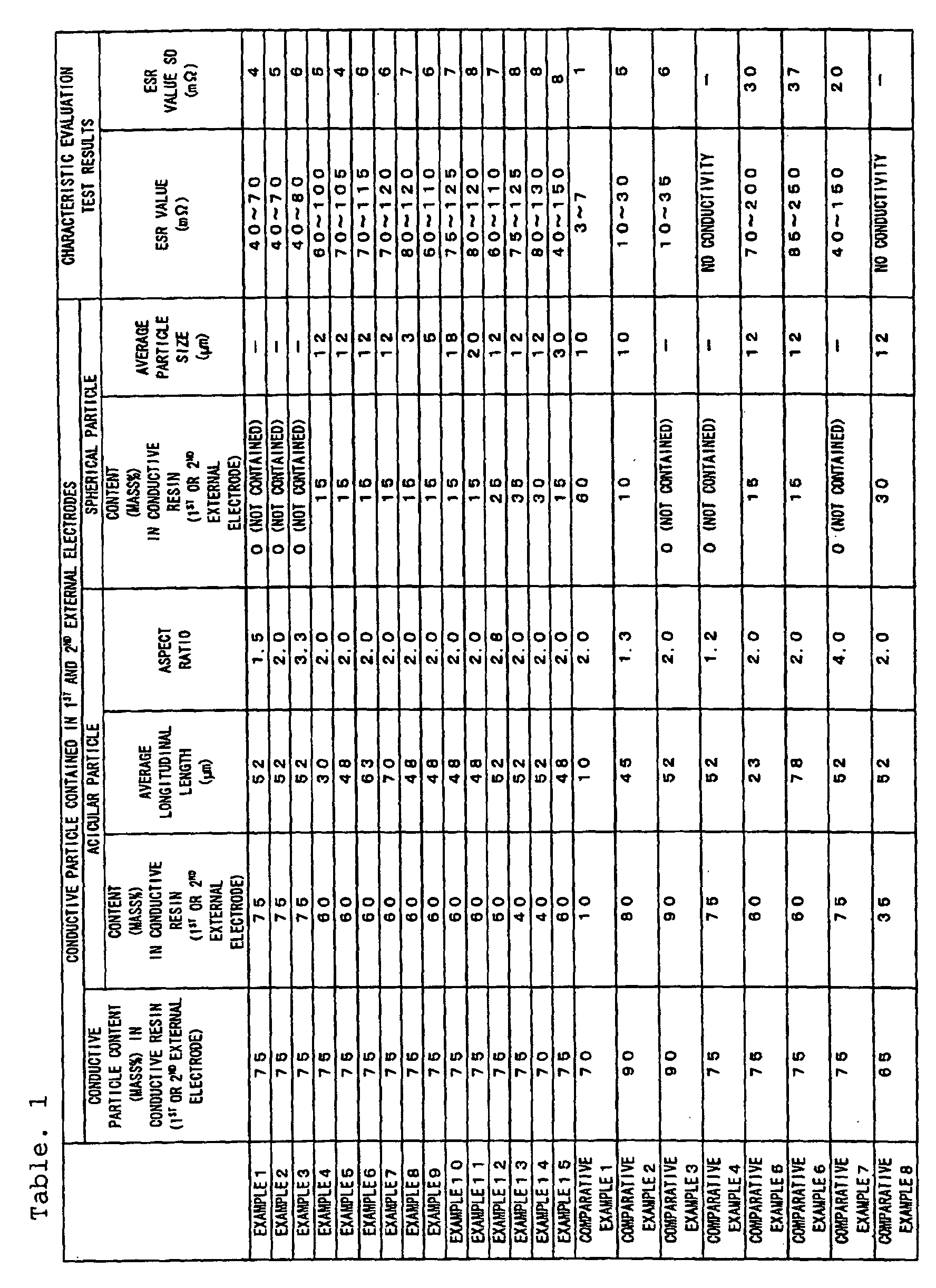
- the conductive particle content in each of the resin electrode layers in the first and second external electrodes was adjusted to the value shown in Table 1.
- the acicular particles particles made of Ag
- those having the aspect ratio and average longitudinal direction shown in Table 1 were used.
- each of the resin electrode layers in the first and second external electrodes was formed from the above-mentioned conductive resin alone as a constituent material, "the conductive particle content in the first external electrode” equals “the conductive particle content in the conductive resin contained in the first external electrode”, and "the conductive particle content in the second external electrode” equals "the conductive particle content in the conductive resin contained in the second external electrode”.
- Laminated ceramic capacitors were made in the same procedure under the same condition as with Example 1 except that respective conductive particle contents in each of the resin electrode layers in the first and second external electrodes were adjusted to their corresponding values shown in Table 1, and that respective particles having their corresponding aspect ratios and average longitudinal lengths shown in Table 1 were used as the acicular particles (particles made of Ag).
- Laminated ceramic capacitors were made in the same procedure under the same condition as with Example 1 except that respective conductive particle contents in each of the resin electrode layers in the first and second external electrodes were adjusted to their corresponding values shown in Table 1, that respective particles having their corresponding aspect ratios and average longitudinal lengths shown in Table 1 were used as the acicular particles (particles made of Ag), and that respective particles having their corresponding average particle sizes shown in Table 1 were used as spherical particles (particles made of Ag).
- Laminated ceramic capacitors were made in the same procedure under the same condition as with Example 1 except that respective conductive particle contents in each of the resin electrode layers in the first and second external electrodes were adjusted to their corresponding values shown in Table 1, that respective particles having their corresponding aspect ratios and average longitudinal lengths shown in Table 1 were used as the acicular particles (particles made of Ag), and that respective particles having their corresponding average particle sizes shown in Table 1 were used as spherical particles (particles made of Ag).
- Laminated ceramic capacitors were made in the same procedure under the same condition as with Example 1 except that respective conductive particle contents in each of the resin electrode layers in the first and second external electrodes were adjusted to their corresponding values shown in Table 1, and that respective particles having their corresponding aspect ratios and average longitudinal lengths shown in Table 1 were used as the acicular particles (particles made of Ag).
- Laminated ceramic capacitors were made in the same procedure under the same condition as with Example 1 except that respective conductive particle contents in each of the resin electrode layers in the first and second external electrodes were adjusted to their corresponding values shown in Table 1, that respective particles having their corresponding aspect ratios and average longitudinal lengths shown in Table 1 were used as the acicular particles (particles made of Ag), and that respective particles having their corresponding average particle sizes shown in Table 1 were used as spherical particles (particles made of Ag).
- a laminated ceramic capacitor was made in the same procedure under the same condition as with Example 1 except that the conductive particle content in each of the resin electrode layers in the first and second external electrodes was adjusted to the value shown in Table 1, and that particles having the aspect ratio and average longitudinal length shown in Table 1 were used as the acicular particles (particles made of Ag).
- a laminated ceramic capacitor was made in the same procedure under the same condition as with Example 1 except that the conductive particle content in each of the resin electrode layers in the first and second external electrodes was adjusted to the value shown in Table 1, that particles having the aspect ratio and average longitudinal length shown in Table 1 were used as the acicular particles (particles made of Ag), and that particles having the average particle size shown in Table 1 were used as spherical particles (particles made of Ag).
- Each of the laminated ceramic capacitors in accordance with Examples 1 to 14 and Comparative Examples 1 to 8 was connected to a measurement terminal of a measuring device of an impedance analyzer (made by Hewlett-Packard Co. under the product name of 4294A), so as to measure its ESR value.
- the frequency was swept once over the range from 100 Hz to 100 MHz, and the value at a self-resonance frequency f0 was determined as the ESR value.
- 10 measurement operations were carried out, so as to calculate the arithmetic average value of ESR values and their standard deviation. The results are shown in Table 1.
- the laminated ceramic capacitors in accordance with Examples 1 to 15 can yield laminated ceramic capacitors having an ESR value within a wide range of 40 to 150 m ⁇ with a standard deviation of 10 m ⁇ or less in the ESR value, which can sufficiently be used in a smoothing circuit of a power supply circuit, etc.
- the present invention can easily and reliably yield a laminate type electronic component having an ESR value of 40 to 150 m ⁇ with a fluctuation (standard deviation) of 10 m ⁇ or less in the ESR value at the time of operation.
- This can provide a laminate type electronic component having such an excellent reliability that the oscillation phenomenon can sufficiently be prevented from occurring and a sufficient smoothing action can be obtained even when used in a power supply bypass circuit, while having a configuration excellent in mass productivity.
Landscapes
- Engineering & Computer Science (AREA)
- Power Engineering (AREA)
- Manufacturing & Machinery (AREA)
- Microelectronics & Electronic Packaging (AREA)
- Fixed Capacitors And Capacitor Manufacturing Machines (AREA)
- Ceramic Capacitors (AREA)
Abstract
Description
wherein at least one of the at least two internal electrodes is electrically connected to the first external electrode, and at least one of the at least two internal electrodes is electrically connected to the second external electrode;
wherein each of the first and second external electrodes comprises at least a resin electrode layer made of a conductive resin mainly composed of a thermosetting resin and a conductive particle;
wherein the conductive resin has a conductive particle content of 70 to 75 mass%; and
wherein the conductive particle contains an acicular particle having an average longitudinal length of 30 to 70 µm and an aspect ratio of 1.5 to 3.3 as a main ingredient.
Claims (12)
- A laminate type electronic component comprising at least:wherein the dielectric part comprises at least two internal electrodes each electrically connected to one of the first and second external electrodes, and at least one dielectric layer made of the dielectric and disposed one by one between electrodes adjacent each other in the at least two internal electrodes;a dielectric part containing a dielectric as a constituent material; anda pair of first and second external electrodes, each disposed in close contact with the dielectric part, opposing each other by way of the dielectric part;
wherein at least one of the at least two internal electrodes is electrically connected to the first external electrode, and at least one of the at least two internal electrodes is electrically connected to the second external electrode;
wherein each of the first and second external electrodes comprises at least a resin electrode layer made of a conductive resin mainly composed of a thermosetting resin and a conductive particle;
wherein the conductive resin has a conductive particle content of 70 to 75 mass%; and
wherein the conductive particle contains an acicular particle having an average longitudinal length of 30 to 70 µm and an aspect ratio of 1.5 to 3.3 as a main ingredient. - The laminate type electronic component according to claim 1, wherein the acicular particle contained in the conductive resin has a content of 40 to 75 mass% therein.
- The laminate type electronic component according to claim 1, wherein the conductive particle further contains a spherical particle having an average particle size of 3 to 20 µm;
wherein the acicular particle has a content of 40 to 75 mass% in the conductive particle; and
wherein the spherical particle has a content of 15 to 35 mass% in the conductive particle. - The laminate type electronic component according to claim 1, wherein the acicular particle is a particle comprising Ag.
- The laminate type electronic component according to claim 1, wherein the spherical particle is a particle comprising Ag.
- The laminate type electronic component according to claim 1, wherein each of the first and second external electrodes is further provided with a metal electrode layer comprising a metal disposed between the resin electrode layer and dielectric part.
- The laminate type electronic component according to claim 6, wherein the metal electrode layer is formed by sintering a paste mainly composed of any of metals of Cu, Ag, Pd, Ni, and Ag-Pd alloy.
- The laminate type electronic component according to claim 1, wherein a Ni plating layer formed from Ni by plating is further disposed on an outer surface of the resin electrode layer.
- The laminate type electronic component according to claim 1, wherein an Sn plating layer formed from Sn by plating is further disposed on an outer surface of the Ni plating layer.
- The laminate type electronic component according to claim 1, wherein the at least two internal electrodes are disposed in the dielectric part such that one of the two internal electrodes adjacent each other by way of the dielectric layer is electrically connected to the first external electrode whereas the other is electrically connected to the second external electrode.
- The laminate type electronic component according to claim 1, having an equivalent series resistance value of 40 to 150 mΩ with a standard deviation of 10 mΩ or less in the equivalent series resistance value obtained at the time of operation.
- The laminate type electronic component according to claim 10, wherein the standard deviation of the equivalent series resistance value is 8 mΩ or less.
Applications Claiming Priority (3)
| Application Number | Priority Date | Filing Date | Title |
|---|---|---|---|
| JP2002061663 | 2002-03-07 | ||
| JP2002061663 | 2002-03-07 | ||
| PCT/JP2003/002743 WO2003075295A1 (en) | 2002-03-07 | 2003-03-07 | Laminate type electronic component |
Publications (3)
| Publication Number | Publication Date |
|---|---|
| EP1482524A1 true EP1482524A1 (en) | 2004-12-01 |
| EP1482524A4 EP1482524A4 (en) | 2008-08-27 |
| EP1482524B1 EP1482524B1 (en) | 2011-09-28 |
Family
ID=27784865
Family Applications (1)
| Application Number | Title | Priority Date | Filing Date |
|---|---|---|---|
| EP03743633A Expired - Lifetime EP1482524B1 (en) | 2002-03-07 | 2003-03-07 | Laminate type electronic component |
Country Status (6)
| Country | Link |
|---|---|
| US (1) | US6956731B2 (en) |
| EP (1) | EP1482524B1 (en) |
| JP (1) | JP4276084B2 (en) |
| CN (1) | CN100428378C (en) |
| TW (1) | TWI269325B (en) |
| WO (1) | WO2003075295A1 (en) |
Cited By (2)
| Publication number | Priority date | Publication date | Assignee | Title |
|---|---|---|---|---|
| US9583265B2 (en) | 2013-10-02 | 2017-02-28 | Samsung Electro-Mechanics Co., Ltd. | Multilayer ceramic electronic component and method of manufacturing the same |
| US9666366B2 (en) | 2002-04-15 | 2017-05-30 | Avx Corporation | Method of making multi-layer electronic components with plated terminations |
Families Citing this family (32)
| Publication number | Priority date | Publication date | Assignee | Title |
|---|---|---|---|---|
| US7286368B2 (en) * | 2004-10-29 | 2007-10-23 | Intel Corporation | System to control effective series resistance of decoupling capacitor |
| JP2007234800A (en) | 2006-02-28 | 2007-09-13 | Tdk Corp | Electronic component and manufacturing method thereof |
| JP2008085280A (en) * | 2006-09-26 | 2008-04-10 | Taiyo Yuden Co Ltd | Surface-mounting electronic component and manufacturing method thereof |
| CN101656152B (en) * | 2008-08-19 | 2011-08-17 | 达方电子股份有限公司 | Multilayer ceramic capacitor and method of forming same |
| US20130107419A1 (en) * | 2011-10-28 | 2013-05-02 | Kemet Electronics Corporation | Multilayered ceramic capacitor with improved lead frame attachment |
| JP5794222B2 (en) * | 2012-02-03 | 2015-10-14 | 株式会社村田製作所 | Ceramic electronic components |
| KR101792268B1 (en) * | 2012-03-13 | 2017-11-01 | 삼성전기주식회사 | Multilayered ceramic capacitor |
| KR101565639B1 (en) * | 2013-02-20 | 2015-11-03 | 삼성전기주식회사 | Multi-layered ceramic electronic parts |
| KR101444615B1 (en) * | 2013-08-09 | 2014-09-26 | 삼성전기주식회사 | Multi-layered ceramic capacitor and manufacturing method the same |
| KR102097329B1 (en) * | 2013-09-12 | 2020-04-06 | 삼성전기주식회사 | Multi-layered ceramic capacitor, manufacturing method thereof and board for mounting the same |
| JP2015026840A (en) * | 2013-10-25 | 2015-02-05 | 株式会社村田製作所 | Ceramic electronic component and taping electronic component series |
| JP6502627B2 (en) * | 2014-07-29 | 2019-04-17 | 太陽誘電株式会社 | Coil parts and electronic devices |
| KR102025708B1 (en) * | 2014-08-11 | 2019-09-26 | 삼성전기주식회사 | Chip electronic component and board having the same mounted thereon |
| JP6639823B2 (en) | 2015-01-13 | 2020-02-05 | 三菱マテリアル電子化成株式会社 | Silver-coated resin particles, method for producing the same, and conductive paste using the same |
| KR20160125121A (en) * | 2015-04-21 | 2016-10-31 | 삼성전기주식회사 | Multi-layered ceramic capacitor and manufacturing method the same |
| KR101983183B1 (en) * | 2015-06-15 | 2019-05-28 | 삼성전기주식회사 | Multi-layered ceramic electronic parts and fabricating method thereof |
| JP6623574B2 (en) * | 2015-06-24 | 2019-12-25 | 株式会社村田製作所 | Multilayer ceramic capacitors |
| CN106571229B (en) * | 2015-10-09 | 2018-11-09 | 株式会社村田制作所 | Electronic unit |
| KR102242667B1 (en) | 2015-12-22 | 2021-04-21 | 삼성전기주식회사 | Multi-layered ceramic electronic parts and fabricating method thereof |
| US10580567B2 (en) | 2016-07-26 | 2020-03-03 | Samsung Electro-Mechanics Co., Ltd. | Coil component and method of manufacturing the same |
| JP2018110185A (en) * | 2017-01-04 | 2018-07-12 | 株式会社村田製作所 | Method for manufacturing multilayer ceramic capacitor, ceramic laminate, and multilayer ceramic capacitor |
| TWI665691B (en) * | 2017-01-25 | 2019-07-11 | 禾伸堂企業股份有限公司 | Multilayer ceramic capacitor and its manufacturing method |
| KR20180093464A (en) * | 2017-02-13 | 2018-08-22 | 삼성전기주식회사 | Common mode filter |
| JP6972592B2 (en) * | 2017-03-16 | 2021-11-24 | Tdk株式会社 | Electronic components and electronic component equipment |
| KR102463330B1 (en) * | 2017-10-17 | 2022-11-04 | 삼성전기주식회사 | Coil Electronic Component |
| KR20190121213A (en) * | 2018-10-24 | 2019-10-25 | 삼성전기주식회사 | Ceramic electronic component |
| WO2020174847A1 (en) * | 2019-02-28 | 2020-09-03 | 株式会社村田製作所 | Electronic component and method for manufacturing electronic component |
| KR102130678B1 (en) | 2019-04-16 | 2020-07-06 | 삼성전기주식회사 | Coil Electronic Component |
| KR102803446B1 (en) | 2019-09-04 | 2025-05-07 | 삼성전기주식회사 | Multilayered electronic component |
| KR102154199B1 (en) * | 2019-09-11 | 2020-09-09 | 삼성전기주식회사 | Chip electronic component and board having the same mounted thereon |
| JP7385469B2 (en) * | 2019-12-27 | 2023-11-22 | 太陽誘電株式会社 | electronic components |
| JP2022067931A (en) * | 2020-10-21 | 2022-05-09 | Tdk株式会社 | Electronic component |
Family Cites Families (19)
| Publication number | Priority date | Publication date | Assignee | Title |
|---|---|---|---|---|
| JPS59225509A (en) | 1983-06-06 | 1984-12-18 | 日本電気株式会社 | Cr composite unit |
| JPS61106408A (en) * | 1984-10-25 | 1986-05-24 | Daikin Ind Ltd | Preparation of acicular particle containing iron carbide |
| JPH01315903A (en) * | 1988-06-14 | 1989-12-20 | Tdk Corp | Electricaly conductive paste and chip parts |
| US5252380A (en) * | 1988-10-31 | 1993-10-12 | Hitachi Maxell, Ltd. | Acicular alloy containing magnetic recording medium |
| US5137783A (en) * | 1989-04-07 | 1992-08-11 | Toda Kogyo Corporation | Acicular magnetic metal particles containing iron as main ingredient and process for producing the same |
| JP2578264B2 (en) | 1991-05-15 | 1997-02-05 | 太陽誘電株式会社 | Adjustment method of equivalent series resistance of ceramic capacitor |
| JPH06267784A (en) * | 1992-11-04 | 1994-09-22 | Du Pont Kk | Conductive resin paste and multilayer ceramic chip capacitor having terminal electrodes made of the same |
| JPH0845784A (en) | 1994-07-26 | 1996-02-16 | Taiyo Yuden Co Ltd | Manufacture of compound electronic component |
| JP3599149B2 (en) * | 1996-08-21 | 2004-12-08 | 日立化成工業株式会社 | Conductive paste, electric circuit using conductive paste, and method of manufacturing electric circuit |
| JPH10284343A (en) * | 1997-04-11 | 1998-10-23 | Mitsubishi Materials Corp | Chip type electronic components |
| JPH10321460A (en) | 1997-05-20 | 1998-12-04 | Matsushita Electric Ind Co Ltd | External electrode of capacitor element and method of manufacturing the same |
| JPH10316901A (en) * | 1997-05-22 | 1998-12-02 | Toyoda Gosei Co Ltd | Electroconductive coating material |
| JPH1154358A (en) | 1997-07-30 | 1999-02-26 | Kyocera Corp | Multilayer ceramic capacitors |
| JPH11162771A (en) | 1997-11-25 | 1999-06-18 | Kyocera Corp | Multilayer ceramic capacitors |
| JP2000138130A (en) | 1998-11-02 | 2000-05-16 | Kyocera Corp | Chip type electronic components |
| JP3376971B2 (en) * | 1999-09-09 | 2003-02-17 | 株式会社村田製作所 | Ceramic electronic components |
| JP3534684B2 (en) * | 2000-07-10 | 2004-06-07 | Tdk株式会社 | Conductive paste, external electrode and method of manufacturing the same |
| JP2002057423A (en) * | 2000-08-07 | 2002-02-22 | Matsushita Electric Ind Co Ltd | Circuit board using conductive paste and method of manufacturing the same |
| JP2002234769A (en) * | 2001-02-01 | 2002-08-23 | Murata Mfg Co Ltd | Method for producing barium titanate powder, barium titanate powder, dielectric ceramic and multilayer ceramic capacitor |
-
2003
- 2003-03-07 JP JP2003573659A patent/JP4276084B2/en not_active Expired - Lifetime
- 2003-03-07 TW TW092104907A patent/TWI269325B/en not_active IP Right Cessation
- 2003-03-07 CN CNB038052024A patent/CN100428378C/en not_active Expired - Lifetime
- 2003-03-07 US US10/506,812 patent/US6956731B2/en not_active Expired - Lifetime
- 2003-03-07 WO PCT/JP2003/002743 patent/WO2003075295A1/en not_active Ceased
- 2003-03-07 EP EP03743633A patent/EP1482524B1/en not_active Expired - Lifetime
Cited By (5)
| Publication number | Priority date | Publication date | Assignee | Title |
|---|---|---|---|---|
| US9666366B2 (en) | 2002-04-15 | 2017-05-30 | Avx Corporation | Method of making multi-layer electronic components with plated terminations |
| US10020116B2 (en) | 2002-04-15 | 2018-07-10 | Avx Corporation | Plated terminations |
| US10366835B2 (en) | 2002-04-15 | 2019-07-30 | Avx Corporation | Plated terminations |
| US11195659B2 (en) | 2002-04-15 | 2021-12-07 | Avx Corporation | Plated terminations |
| US9583265B2 (en) | 2013-10-02 | 2017-02-28 | Samsung Electro-Mechanics Co., Ltd. | Multilayer ceramic electronic component and method of manufacturing the same |
Also Published As
| Publication number | Publication date |
|---|---|
| EP1482524B1 (en) | 2011-09-28 |
| US20050083637A1 (en) | 2005-04-21 |
| US6956731B2 (en) | 2005-10-18 |
| WO2003075295A1 (en) | 2003-09-12 |
| TWI269325B (en) | 2006-12-21 |
| JPWO2003075295A1 (en) | 2005-06-30 |
| EP1482524A4 (en) | 2008-08-27 |
| CN100428378C (en) | 2008-10-22 |
| JP4276084B2 (en) | 2009-06-10 |
| CN1639815A (en) | 2005-07-13 |
| TW200401313A (en) | 2004-01-16 |
Similar Documents
| Publication | Publication Date | Title |
|---|---|---|
| EP1482524B1 (en) | Laminate type electronic component | |
| CN101042960B (en) | Capacitor assembly | |
| US6185091B1 (en) | Four-terminal capacitor | |
| EP2411988B1 (en) | Leaded multi-layer ceramic capacitor with low esl and low esr | |
| US20180061571A1 (en) | Multilayer ceramic electronic component and method of manufacturing the same | |
| US20080128860A1 (en) | Monolithic electronic component | |
| KR101983128B1 (en) | Multilayer Ceramic Electronic Component | |
| US20020039272A1 (en) | Reduction-resistant dielectric ceramic compact and laminated ceramic capacitor | |
| JP2001189233A (en) | Layered capacitor | |
| CN104658756A (en) | Multilayer Ceramic Electronic Component And Board Having The Same Mounted Thereon | |
| EP3226270B1 (en) | Solid electrolytic capacitor | |
| KR20150049795A (en) | Multi-layered ceramic capacitor and board for mounting the same | |
| JP2021141323A (en) | Leadless stacked ceramic capacitor | |
| KR101532116B1 (en) | Multi-Layered Ceramic Electronic Component and Manufacturing Method of the Same | |
| JP2000173860A (en) | Composite capacitor | |
| US12148570B2 (en) | Multilayer electronic component | |
| Engel | Material requirements for power and high temperature multilayer ceramic capacitors (MLCC) | |
| JP6904505B2 (en) | Dielectric porcelain composition and multilayer ceramic capacitors containing it | |
| CN120164726B (en) | A multilayer ceramic capacitor and its preparation method | |
| EP4557333A1 (en) | Multilayer ceramic capacitor | |
| JP3822714B2 (en) | CR composite electronic component and manufacturing method thereof | |
| US20250166910A1 (en) | Multilayer electronic component | |
| US20260058065A1 (en) | Multilayer electronic component | |
| EP4579700A1 (en) | Multilayer electronic component | |
| EP4435811A2 (en) | Multilayer electronic component |
Legal Events
| Date | Code | Title | Description |
|---|---|---|---|
| PUAI | Public reference made under article 153(3) epc to a published international application that has entered the european phase |
Free format text: ORIGINAL CODE: 0009012 |
|
| 17P | Request for examination filed |
Effective date: 20040907 |
|
| AK | Designated contracting states |
Kind code of ref document: A1 Designated state(s): AT BE BG CH CY CZ DE DK EE ES FI FR GB GR IE IT LI LU MC NL PT RO SE SI SK TR |
|
| AX | Request for extension of the european patent |
Extension state: AL LT LV MK |
|
| A4 | Supplementary search report drawn up and despatched |
Effective date: 20080724 |
|
| RIC1 | Information provided on ipc code assigned before grant |
Ipc: H01G 4/232 20060101AFI20080718BHEP |
|
| GRAP | Despatch of communication of intention to grant a patent |
Free format text: ORIGINAL CODE: EPIDOSNIGR1 |
|
| GRAS | Grant fee paid |
Free format text: ORIGINAL CODE: EPIDOSNIGR3 |
|
| GRAA | (expected) grant |
Free format text: ORIGINAL CODE: 0009210 |
|
| AK | Designated contracting states |
Kind code of ref document: B1 Designated state(s): DE |
|
| REG | Reference to a national code |
Ref country code: DE Ref legal event code: R096 Ref document number: 60338545 Country of ref document: DE Effective date: 20111208 |
|
| PLBE | No opposition filed within time limit |
Free format text: ORIGINAL CODE: 0009261 |
|
| STAA | Information on the status of an ep patent application or granted ep patent |
Free format text: STATUS: NO OPPOSITION FILED WITHIN TIME LIMIT |
|
| 26N | No opposition filed |
Effective date: 20120629 |
|
| REG | Reference to a national code |
Ref country code: DE Ref legal event code: R097 Ref document number: 60338545 Country of ref document: DE Effective date: 20120629 |
|
| PGFP | Annual fee paid to national office [announced via postgrant information from national office to epo] |
Ref country code: DE Payment date: 20220203 Year of fee payment: 20 |
|
| REG | Reference to a national code |
Ref country code: DE Ref legal event code: R071 Ref document number: 60338545 Country of ref document: DE |