EP1482297A1 - Scanning probe microscope and specimen surface structure measuring method - Google Patents
Scanning probe microscope and specimen surface structure measuring method Download PDFInfo
- Publication number
- EP1482297A1 EP1482297A1 EP03703178A EP03703178A EP1482297A1 EP 1482297 A1 EP1482297 A1 EP 1482297A1 EP 03703178 A EP03703178 A EP 03703178A EP 03703178 A EP03703178 A EP 03703178A EP 1482297 A1 EP1482297 A1 EP 1482297A1
- Authority
- EP
- European Patent Office
- Prior art keywords
- probe
- specimen
- cantilever
- specimen surface
- frequency
- Prior art date
- Legal status (The legal status is an assumption and is not a legal conclusion. Google has not performed a legal analysis and makes no representation as to the accuracy of the status listed.)
- Withdrawn
Links
Images




Classifications
-
- G—PHYSICS
- G01—MEASURING; TESTING
- G01Q—SCANNING-PROBE TECHNIQUES OR APPARATUS; APPLICATIONS OF SCANNING-PROBE TECHNIQUES, e.g. SCANNING PROBE MICROSCOPY [SPM]
- G01Q60/00—Particular types of SPM [Scanning Probe Microscopy] or microscopes; Essential components thereof
- G01Q60/24—AFM [Atomic Force Microscopy] or apparatus therefor, e.g. AFM probes
- G01Q60/32—AC mode
- G01Q60/34—Tapping mode
-
- G—PHYSICS
- G01—MEASURING; TESTING
- G01Q—SCANNING-PROBE TECHNIQUES OR APPARATUS; APPLICATIONS OF SCANNING-PROBE TECHNIQUES, e.g. SCANNING PROBE MICROSCOPY [SPM]
- G01Q10/00—Scanning or positioning arrangements, i.e. arrangements for actively controlling the movement or position of the probe
- G01Q10/04—Fine scanning or positioning
- G01Q10/06—Circuits or algorithms therefor
-
- G—PHYSICS
- G01—MEASURING; TESTING
- G01Q—SCANNING-PROBE TECHNIQUES OR APPARATUS; APPLICATIONS OF SCANNING-PROBE TECHNIQUES, e.g. SCANNING PROBE MICROSCOPY [SPM]
- G01Q30/00—Auxiliary means serving to assist or improve the scanning probe techniques or apparatus, e.g. display or data processing devices
- G01Q30/04—Display or data processing devices
-
- G—PHYSICS
- G01—MEASURING; TESTING
- G01Q—SCANNING-PROBE TECHNIQUES OR APPARATUS; APPLICATIONS OF SCANNING-PROBE TECHNIQUES, e.g. SCANNING PROBE MICROSCOPY [SPM]
- G01Q70/00—General aspects of SPM probes, their manufacture or their related instrumentation, insofar as they are not specially adapted to a single SPM technique covered by group G01Q60/00
- G01Q70/08—Probe characteristics
- G01Q70/10—Shape or taper
- G01Q70/12—Nanotube tips
-
- B—PERFORMING OPERATIONS; TRANSPORTING
- B82—NANOTECHNOLOGY
- B82Y—SPECIFIC USES OR APPLICATIONS OF NANOSTRUCTURES; MEASUREMENT OR ANALYSIS OF NANOSTRUCTURES; MANUFACTURE OR TREATMENT OF NANOSTRUCTURES
- B82Y15/00—Nanotechnology for interacting, sensing or actuating, e.g. quantum dots as markers in protein assays or molecular motors
Definitions
- the present invention relates to a scanning probe microscope capable of making three-dimensional measurements on the nanometer order of accuracy on the surface structure of a specimen, and relates in particular to a probe microscope capable of accurate measurements of a surface structure with a fine structure on the nanometer level, and further possessing a high aspect ratio.
- SEM scanning electron microscope
- FIB focusing ion beam
- These types of methods using probe microscopes to measure surface structures with high aspect ratios include a method (Patent No. 2936545) for discrete scanning of the specimen in a state where the probe is separated from the specimen, and the probe is moved to a measurement point in proximity to the specimen to measure the surface position.
- a method for discrete scanning of the specimen in a state where the probe is separated from the specimen, and the probe is moved to a measurement point in proximity to the specimen to measure the surface position.
- the gap between the specimen and probe when making an actual physical measurement is larger than necessary and the probe moves at high speed to the next pixel; and when making surface measurements, the scanning is stopped, and the probe is moved in proximity to the specimen and measures the surface position.
- Measurements of a specimen surfaces with a large aspect ratio and small aperture diameter require attaching an extremely slim probe as a tip of the cantilever.
- the elasticity (spring constant) of the probe is therefore poor horizontally and is nearly the same spring constant as the cantilever.
- the probe therefore warps or deforms on reaching the oblique surface (of the specimen).
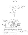
- F c is the fixed atomic force
- ⁇ is the angle the oblique surface tilts from perpendicular relative to the probe
- k is the spring constant of the probe
- E is the Young's modulus of the probe
- 1 is the probe length
- t is the probe thickness.
- the ⁇ a is here called the probe aspect ratio.
- the probe aspect ratio holds roughly the same significance as the specimen aspect ratio. This type of measurement cannot be performed unless the probe aspect ratio is higher than the specimen aspect ratio.
- the force setting is approximately 10 -8 N.
- the angle ⁇ is 45 degrees
- the Young's modulus E of the probe is 2 ⁇ 10 11 N/cm 2
- the probe length l is 1 ⁇ m
- the ⁇ r and the ⁇ z are 2 nanometers.
- the angle ⁇ is 80 degrees
- the ⁇ r is 11 nanometers and the ⁇ z is 64 nanometers.
- the present invention has the object of providing a scanning probe microscope capable of accurately measuring surface structures with high aspect ratio, and a method for measuring surface structures of specimens having a high aspect ratio.
- the present invention employs the vibration type force detection method.
- the present invention uses a non-contact force detection method.
- the cantilever supporting the probe is oscillated at its resonance point, and the shift occurring in the resonance point (resonance frequency) due to an externally applied force is measured.
- One type (FM modulation type) detects the weak force acting on the probe by oscillating the cantilever supporting the probe at its resonance point and measuring the shift in the resonance point due to an externally applied force.
- the other type oscillates the cantilever at a frequency slightly shifted from its resonance point, and measures the minuscule atomic force by measuring the change in amplitude resulting from the externally applied force.
- the atomic force in the attraction force region is detected by utilizing these methods.
- An atomic force of around 10 -13 N can be detected by these methods.
- a probe position error of 1 nanometer or less can be attained even with a slope of 85 degrees or more on the specimen cross section so that shapes with an aspect ratio of 10 or more can be measured with accuracy on the sub-nanometer level.
- High aspect probes such as carbon nanotubes can also be used as probes in this invention.
- the scanning probe microscope of the present invention is in other words, characterized in comprising: a specimen stage for mounting the specimen, a probe, a cantilever for supporting the probe, a first probe movement means for moving the probe two-dimensionally along the surface of the specimen, a second probe movement means for moving the probe closer to or farther away from the specimen surface, a probe position detection means for detecting the probe position, a means to oscillate the cantilever at a specified frequency shifted slightly from the cantilever resonance point, an amplitude detection means to detect the oscillation amplitude of the specified frequency component of the cantilever, and a control means to detect changes in the vibration amplitude while moving the cantilever closer to the specimen surface and measure the probe position when the change in the vibration amplitude has reached a specified quantity.
- the amplitude detection means is comprised of a lock-in amplifier.
- the scanning probe microscope of the present invention is further characterized in comprising: a specimen stage for mounting the specimen, a probe, a cantilever for supporting the probe, a first probe movement means for moving the probe two-dimensionally along the surface of the specimen, a second probe movement means for moving the probe closer to or farther away from the specimen surface, a probe position detection means for detecting the probe position, a means to oscillate the cantilever supporting the probe at that resonance point, a resonance frequency shift detection means to detect a shift in the resonance frequency of the cantilever, and a control means to detect a shift in the resonance frequency of the cantilever while moving the cantilever in a direction closer to the specimen surface, and measure the probe position when the shift in the resonance frequency reaches a specified quantity.
- the resonance frequency shift detection means may be comprised of a phase-locked-loop circuit.
- the probe of the scanning probe microscope of the present invention may be comprised of carbon nanotube.
- the probe position detection means may utilize a capacity displacement meter a strain gauge, a light interferometer or an optical lever.
- the specimen surface structure measuring method of the present invention for measuring the surface structure of the specimen utilizing the scanning probe microscope containing a cantilever supporting the probe, with this measuring method comprising: a step to stop the servo system maintaining a fixed gap between the probe and specimen and move the probe along the specimen surface to the measurement point with the probe separate from the specimen, a step to oscillate and move the probe close to the specimen surface and measure the probe position when a specified atomic force is detected in an attraction force region, and a step to move the prove away from the specimen surface immediately after the measurement, and the above steps are repeated at each measurement point.
- the probe is lifted with a distance or more where there is no absorption force to attract the probe.
- the servo circuit (circuit to control the distance between the specimen and probe to attain the desired atomic force) preferably utilizes a distance control signal when moving the probe in proximity to the surface of the specimen.
- the probe should also preferably move towards the specimen at a constant speed. Using the servo circuit signal to avoid the probe striking the specimen for the probe approach to the surface is essential at this time.
- the probe vibration frequency is a frequency shifted slightly from the resonance point of the cantilever, and the specified atomic force is detected based on the change in the vibration amplitude of the cantilever.
- the vibration frequency of the probe may be made the cantilever resonance point frequency and, the atomic force detected based on the shift in the cantilever resonance frequency.
- the scanning probe microscope of the present invention may be used for measurement of tiny devices or may be used to measure defects. This scanning probe microscope may also be used as a line monitor in the semiconductor manufacturing process.
- the vibration method (non-contact) method is used simultaneous with probe operation at a force setting of 10 -10 N and below. Therefore, even with an aspect ratio of 10 or more, errors of 1 nanometer or less due to slip of the probe can be suppressed, and high precision shape measurement can be performed.
- FIG. 1 is a block diagram showing an example of the digital probing AFM of the present invention using the slope detection method.
- this digital probing AFM contains a vibration mechanism for detecting the atomic force gradient.
- the specimen 11 is mounted on the XY specimen stage 12.
- the XY specimen stage 12 is moved coarsely by the XY scanning circuit 25 so that the measurement region is selected directly below the probe.
- the cantilever 22 with the probe is attached on an exciter piezoelectric element 23 and a cylindrical XYZ scanning piezoelectric element 24.
- a normal optical lever method made up of a semiconductor laser 31, a position detector 32, and a force detector 34 is utilized as the force detector.
- the servo circuit 35 drives the probe in the Z direction by means of the XYZ scanning piezoelectric element 24, and servo controls the force to a fixed value with the signal detected by force detector 34.
- the XY scanning circuit 25 performs XY scanning utilizing the XYZ scanning piezoelectric element 24 for drive of the probe in the XY directions along the specimen surface. Though not shown in the drawing, an approach is installed for making the probe approach or retract from the surface of the specimen 11 with a large stroke from Z movement of the XYZ scanning piezoelectric element 24.
- the present example utilizes a lock-in amplifier 40 for detecting the force gradient.
- the controller 37 controls the XY scanning circuit 24 and the servo circuit 35.
- the probe preferably has a shape and slim shape as possible in view of the height and groove depth of the specimen 11.
- probes with an aspect ratio of 10 or more are preferably fabricated using a carbon nanotube or carbon fiber, etc.
- FIG. 2 is concept drawing showing an example of the probe of carbon nanotube.
- a carbon nanotube forming the probe 21 is bonded to the tip of the cantilever 22 made from silicon film, silicon nitride film or silicon oxide film.
- the diameter of the carbon nanotube is preferably approximately 10 to 50 nanometers and the length is 500 nanometers or more.
- the carbon nanotube is attached to the cantilever 22 by adhering the carbon nanotube to the tip of the cantilever supporting to a manipulator not shown in the drawing.
- the electron beam is then irradiated onto the end section (arrow position in drawing) cantilever 22 side of the carbon nanotube, and the bonding (adhesion) is performed by means electron beam deposition of the carbon at that time.
- FIG. 3 is a drawing showing the movement of the probe during the measurement sequence in vibration type digital probing AFM shown in FIG. 1.
- FIG. 3(a) is a drawing showing the repeated movement of the probe along the specimen surface.
- FIG. 3(b) is a drawing showing the fundamental movement of the probe for one pixel point.
- the probe 21 is first of all driven approximately a few to a few hundred nanometers in the Z direction while vibrated by the XYZ scanning piezoelectric element 24 and is made to approach the surface of the specimen 11.
- An excitation signal is at this time output from the lock-in amplifier 40 or an external oscillator, and input to the exciter piezoelectric element 23.
- the vibration of the exciter piezoelectric element 23 then vibrates the probe 21.
- the vibration frequency is a frequency shifted slightly from the cantilever resonance point.
- the probe 21 is then lifted up in a pre-determined distance ⁇ Z to retract it from the specimen surface (2).
- This distance ⁇ Z is at least a distance where the specimen 11 has no absorption force on the probe 2, or is set as a distance larger than the predicted surface irregularities.
- the XY scanning circuit 25 next drives the XYZ scanning piezoelectric element 24 to move the probe only by ⁇ X in the X direction, and sets the probe 21 at the next pixel position (3).
- the surface structure of the specimen I 1 is measured by the repeated probe 21 movement comprised of the above (1) (2) (3) steps.
- the probe moves just a specified distance ⁇ Y in the Y direction, and again scans in the X direction.
- the specimen surface can be measured three-dimensionally by repeating these movements.
- the measurement of the atomic force gradient acting on the probe is described next utilizing the block diagram of the lock-in amplifier shown in FIG. 4.
- the high frequency signal output from the oscillator 45 is input to the exciter piezoelectric element 23 and the multiplier 41 of the lock-in amplifier 40.
- the cantilever 22 is driven at a frequency ⁇ by the exciter piezoelectric element 23.
- a laser beam 33 emitted from the semiconductor laser 31 is reflected by the cantilever 22, and is detected by the position detector 32 made up of a dual-split or quad-split optical detector.
- the output from the force detector (laser position detector circuit) 34 is multiplied by the output from the oscillator 45 at multiplier 41 inside the lock-in amplifier 40.
- the amplitude of the frequency component output from the multiplier 41 via the low-pass filter 42, that is synchronized with the oscillator signal is then detected.
- the resonance point (frequency) of the cantilever 22 shifts.
- the lock-in amplifier 40 captures the shift in this resonance point as a change in amplitude of the probe 21 vibration. This amplitude change is detected as a fluctuation of the force gradient, and when the preset change in the force gradient is reached, the probe 21 is determined to have arrived at the surface of specimen 11.
- the controller 37 measures the coordinates of the probe 21 at that time or in other words, measures the surface position coordinates (x, y, z).
- FIG. 5 is graph showing the relation of the amount detected as the change in amplitude by the lock-in amplifier and the distance between the specimen surface and probe.
- the horizontal axis is the gap between the probe and specimen.
- the vertical axis is the amplitude of the frequency ⁇ component detected by the lock-in amplifier.
- the curve A expresses the change in amplitude when the excitation frequency ⁇ was set to a frequency lower than the resonance frequency of probe 21. In this case, the amplitude of the frequency ⁇ component increases when the probe 21 nears the specimen surface.
- curve B the amplitude of the frequency ⁇ component conversely decreases when the probe 21 nears the specimen surface. Therefore, by setting a threshold (value) for the amplitude change, the probe 21 can be decided to have reached the specimen surface when the detected change in amplitude has exceeded that threshold.
- the XY scanning function is completely stopped by the XY scanning circuit 25.
- the probe 21 is promptly retracted from the specimen surface in the Z direction by a specified distance ⁇ Z.
- the probe 21 next moves to the next pixel point by the XY scanning circuit 25 by distance ⁇ X.
- the probe 21 is then again moved near the specimen 11 by the same procedure, and detects the surface position.
- the system can also be operated to detect an extremely small force, so errors due to the probe 21 slipping along a steep slope can be drastically reduced when moving the probe 21 in proximity to the specimen 11.
- the method of the present invention can therefore measure with good accuracy the high aspect structures that will be needed in the future.
- the retraction amount ⁇ Z of probe 21 should preferably be set larger than the height or depth of peaks or grooves on specimen 11, in view of the heights or depths of the surface structure of the specimen 11.
- an optical lever was utilized for detecting the displacement of the probe 21.
- a capacity displacement meter, a strain gauge, or a light interferometer or similar device of the known art in measuring technology may also be utilized.
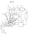
- FIG. 6 is a concept block diagram of showing another example of digital probing AFM in the present invention.
- this digital probing AFM contains an FM (frequency modulation) detection type atomic force gradient detector.
- the force detector utilizes an optical lever system made up of a semiconductor laser 31, a position detector 32, a force detector circuit 34.
- the frequency is demodulated using a PLL (phase-lock-loop) circuit 50 and the change in the force gradient detected from the change in the frequency.
- the servo system, scanning system, proximity mechanism, and probe position detector identical to the first embodiment are utilized to regulate the detected signal to a fixed value.
- an external oscillator or vibrator is not used for self-vibrating the probe, instead a resonance circuit system in the internal circuit network is utilized.
- the closed loop formed by the probe, exciter piezoelectric element 23, oscillator circuit 51, force detector 34 and optical lever probe position detector 32 is made to function as a positive feedback coupling to make the cantilever 22 oscillate (vibrate) at the resonance point.
- the measurement procedure is the same as the first embodiment.
- a closed loop is formed by the probe, exciter piezoelectric element 23, oscillator circuit 51, force detector 34 and light deflection probe position detector 32. These components form a positive feedback coupling to make the cantilever 22 oscillate (vibrate) at the resonance point.
- the probe is made to approach near the specimen surface while being vibrated.
- the preset atomic force gradient acts on the probe, the probe is determined to have made an approach near the specimen surface.
- the surface position information is then acquired and the probe afterwards retracted from the specimen surface to a specified distance ⁇ Z. At the Z position where the probe was retracted, the probe is moved in the X direction to the next pixel position, and the operation for surface position measurement is repeated in the same way.
- the exciter signal from the oscillator circuit 51 is input to the PLL circuit 50 at this time.
- the PLL circuit has a demodulation function, converts the resonance frequency into a low frequency signal, and inputs it to the servo circuit 35.
- the signal V 1 with the resonance frequency ⁇ 1 from oscillator circuit 51 equaling Acos ⁇ 1 t is multiplied by the signal V 2 (Bcos ⁇ 2 t) with a frequency ⁇ 2 from the voltage controlled oscillator 56 at the phase comparator 53.
- the loop filter 54 selects and outputs a signal containing a low frequency component of frequency ( ⁇ 1 - ⁇ 2 ), to the loop amplifier 55.
- the loop amplifier 55 outputs a signal G ⁇ cos( ⁇ 1 - ⁇ 2 )t ⁇ showing the change in frequency.
- FIG. 8 shows the change in resonant frequency detected by the PLL circuit 50, as the probe approaches the specimen surface.
- the fluctuation in the force gradient is detected from this resonant frequency and when the amount of change in the force gradient reaches a preset amount, the probe is determined to have reached the surface of the specimen 11.
- the controller 37 thereupon promptly measures the surface position (x, y, z) of the specimen 11 from the probe position.
- the XY scanning function is completely stopped by the XY scanning circuit 25 at this time.
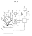
- FIG. 9 is a concept block diagram of a semiconductor scanning device utilizing a digital probing AFM incorporating the slope detection method.
- the semiconductor scanning device shown in the figure contains an AFM having a function using the vibration method for detecting the atomic force gradient.
- This device further contains a chip position detection function for measuring at an optional measurement position within the semiconductor chip, as well as a computer processing function for automatic measurements.
- the force detector for the AFM utilizes the optical lever method.
- This force detector is made up of a semiconductor laser 31, a position detector 32, and a force detector 34.
- a lock-in amplifier 40 detects the force gradient the same as in the first embodiment.
- An approach device (not shown in drawing) is installed to make the probe 21 approach the surface of the specimen 11 (semiconductor chip).
- this embodiment further contains an optical microscope 60 for simultaneously observing the probe 21 and the specimen 11.
- the optical microscope 60 contains an objective lens 61 and an eyepiece lens 62.
- This optical microscope 60 is capable of simultaneously observing the specimen surface and cantilever 22 and the specimen 11.
- the epi-illumination system is omitted from the drawings.
- a CCD camera 63 observes the illuminated specimen 11 and the probe 2.
- the optical target captured by the CCD camera 63 is utilized to accurately recognize the chip position in the system.
- the chip placement on the wafer and the positional relationship within the inspection device are in this way calculated and found. Mapping in this way allows accurately determining the position of the probe 21 on locations on the chip whose surface shape was measured.
- the controller 37 communicates (exchanges data) with the host computer and the wafer auto conveyor robot, receives measurement points and measurement conditions, controls automatic measurement and/or controls carry-in/carry-out of wafers from the robot.
- the controller 37 instructs the XY scanning circuit 25 to drive the specimen stage 12 and the XYZ scanning piezoelectric element 24 so that the location specified by the host computer becomes the observation position, and measures the specified location.
- the controller 37 communicates (transfers) the measurement data to the host computer and displays it on the display device 38.
- the present invention when used to measure the shapes of high aspect structures with dimensions in the submicron range, is capable of making measurements down to the nanometer range and below without the probe slipping on the oblique surface.
- the present invention can further be utilized for defect (flaw) measurement and measuring dimensions of tiny devices.
- the present invention can also be utilized as a line monitor for semiconductor processes.
- the present invention configured as described above, is capable of making measurements down to the nanometer range and below with no slipping of the probe on oblique surfaces in the measuring of shapes of high aspect structures with dimensions in the submicron range.
Landscapes
- Physics & Mathematics (AREA)
- Health & Medical Sciences (AREA)
- General Health & Medical Sciences (AREA)
- General Physics & Mathematics (AREA)
- Nuclear Medicine, Radiotherapy & Molecular Imaging (AREA)
- Radiology & Medical Imaging (AREA)
- Engineering & Computer Science (AREA)
- Power Engineering (AREA)
- Chemical & Material Sciences (AREA)
- Nanotechnology (AREA)
- Length Measuring Devices With Unspecified Measuring Means (AREA)
Abstract
A digital probing type atomic force microscope (AFM) for measuring high
aspect structures with high precision. A probe 21 is vibrated while moved to the
vicinity of an atomic force region on a specimen surface. The position of the probe is
measured when a specified atomic force is detected in the atomic force region. The
probe is then moved away from the specimen surface. A servo system for maintaining
a gap between the probe and specimen surface is stopped. The probe is moved to a
measurement point along the specimen surface while kept away from the specimen.
The vibration frequency is a frequency slightly offset from the cantilever resonance
point. The atomic force is detected based on the vibration amplitude of the cantilever.
Description
The present invention relates to a scanning probe microscope capable of
making three-dimensional measurements on the nanometer order of accuracy on the
surface structure of a specimen, and relates in particular to a probe microscope
capable of accurate measurements of a surface structure with a fine structure on the
nanometer level, and further possessing a high aspect ratio.
In recent years, along with the growth of our information society, there are
increasing needs for technology capable of joint use of large amounts of information.
The semiconductor field is making progress in miniaturization. Current leading edge
technology is seeking to miniaturize devices to a minimum scale of 0.13 µm. Along
with this progress, there is also a need for higher precision and greater miniaturization
in device isolation technology, wiring technology and contact technology, etc.
Structures with a higher aspect ratio (depth/aperture diameter) are also being
proposed and technology to fabricate these structures is being sought. Besides
fabrication technology, advances in measurement technology are also needed. In
particular, development of methods for measuring precision on the nanometer scale
are needed. More specifically, according to the semiconductor road map for the
future, the current minimum hole diameter of 180 nanometers will shrink to 60
nanometers by the year 2010. Also, aspect ratios will increase from 7 to 12 so
measurement down to these dimensions will also become increasingly difficult.
Current technology uses the scanning electron microscope (SEM), to observe a
cross-section of the specimen after splitting it open or machining it with a focusing
ion beam (FIB) technology.
These types of methods using probe microscopes to measure surface
structures with high aspect ratios include a method (Patent No. 2936545) for discrete
scanning of the specimen in a state where the probe is separated from the specimen,
and the probe is moved to a measurement point in proximity to the specimen to
measure the surface position. In this method, during scanning of the surface, the gap
between the specimen and probe when making an actual physical measurement is
larger than necessary and the probe moves at high speed to the next pixel; and when
making surface measurements, the scanning is stopped, and the probe is moved in
proximity to the specimen and measures the surface position.
Measurements of a specimen surfaces with a large aspect ratio and small
aperture diameter require attaching an extremely slim probe as a tip of the cantilever.
The elasticity (spring constant) of the probe is therefore poor horizontally and is
nearly the same spring constant as the cantilever. The probe therefore warps or
deforms on reaching the oblique surface (of the specimen).
In atomic force microscopes (AFM) of the conventional art with contact type
digital probing, the probe at the pixel position, repeatedly moves close to the
specimen surface and then back. When the probe captures the specimen surface while
nearing it, and when the oblique surface is steep, the cantilever 80 and probe 81 are
twisted as shown in FIG. 10, and an error appears in the position measurement on the
surface of the specimen 82. The measurement position error Δr (surface interior) and
Δz (perpendicular direction) are expressed as follows due to the warping of the probe.
Δr = Fc tan/k (k = E1/(5γa 3 ), γa = 1/t)
Δz = Δr tan
Fc = F cos2
Here, Fc is the fixed atomic force, is the angle the oblique surface tilts from
perpendicular relative to the probe, k is the spring constant of the probe, E is the
Young's modulus of the probe, 1 is the probe length, and t is the probe thickness. The
γa is here called the probe aspect ratio. The probe aspect ratio holds roughly the same
significance as the specimen aspect ratio. This type of measurement cannot be
performed unless the probe aspect ratio is higher than the specimen aspect ratio.
In contact type methods for detecting atomic force such as the light deflection
method, the force setting is approximately 10-8N. For example, when the atomic force
Fc setting is 10-8N, the angle is 45 degrees, the Young's modulus E of the probe is
2 × 10¹¹N/cm2, the probe length l is 1 µm, and the probe thickness is 50 nanometers (γa
= 20), then the Δr and the Δz are 2 nanometers. When the angle is 80 degrees, then
the Δr is 11 nanometers and the Δz is 64 nanometers. Further, when the angle is 85
degrees, the Δr is 23 nanometers, the Δz is 261 nanometers, it can be seen that the
probe tip will slip on the specimen surface. This slippage shows that the technology of
the conventional art is not capable of accurately measuring the shape of surface
structures having a high aspect ratio.
In view of the problems with the conventional art, the present invention has
the object of providing a scanning probe microscope capable of accurately measuring
surface structures with high aspect ratio, and a method for measuring surface
structures of specimens having a high aspect ratio.
As can be seen from equations (1) and (2), lowering the atomic force Fc by
regulating it to a fixed quantity with the servo will prove effective in reducing the
measurement position errors Δr and Δz. In other words, it is important that a small
atomic force be used to control the system. The conventional art utilized the atomic
force of the repulsive force region to accomplish this. However, the minimum atomic
force is approximately 10-8N so achieving a measurement position error of 1
nanometer or less, requires setting an atomic force regulated to 10-10N or less.
In order to regulate the atomic force to 10-10N or less, the present invention
employs the vibration type force detection method. In other words, the present
invention uses a non-contact force detection method. In this method, the cantilever
supporting the probe is oscillated at its resonance point, and the shift occurring in the
resonance point (resonance frequency) due to an externally applied force is measured.
There are two types of non-contact force detection methods. One type (FM
modulation type) detects the weak force acting on the probe by oscillating the
cantilever supporting the probe at its resonance point and measuring the shift in the
resonance point due to an externally applied force. The other type (slope detection
method) oscillates the cantilever at a frequency slightly shifted from its resonance
point, and measures the minuscule atomic force by measuring the change in amplitude
resulting from the externally applied force. The atomic force in the attraction force
region is detected by utilizing these methods. An atomic force of around 10-13N can be
detected by these methods. Further, a probe position error of 1 nanometer or less can
be attained even with a slope of 85 degrees or more on the specimen cross section so
that shapes with an aspect ratio of 10 or more can be measured with accuracy on the
sub-nanometer level. High aspect probes such as carbon nanotubes can also be used as
probes in this invention.
The scanning probe microscope of the present invention is in other words,
characterized in comprising: a specimen stage for mounting the specimen, a probe, a
cantilever for supporting the probe, a first probe movement means for moving the
probe two-dimensionally along the surface of the specimen, a second probe movement
means for moving the probe closer to or farther away from the specimen surface, a
probe position detection means for detecting the probe position, a means to oscillate
the cantilever at a specified frequency shifted slightly from the cantilever resonance
point, an amplitude detection means to detect the oscillation amplitude of the
specified frequency component of the cantilever, and a control means to detect
changes in the vibration amplitude while moving the cantilever closer to the specimen
surface and measure the probe position when the change in the vibration amplitude
has reached a specified quantity. The amplitude detection means is comprised of a
lock-in amplifier.
The scanning probe microscope of the present invention is further
characterized in comprising: a specimen stage for mounting the specimen, a probe, a
cantilever for supporting the probe, a first probe movement means for moving the
probe two-dimensionally along the surface of the specimen, a second probe movement
means for moving the probe closer to or farther away from the specimen surface, a
probe position detection means for detecting the probe position, a means to oscillate
the cantilever supporting the probe at that resonance point, a resonance frequency
shift detection means to detect a shift in the resonance frequency of the cantilever, and
a control means to detect a shift in the resonance frequency of the cantilever while
moving the cantilever in a direction closer to the specimen surface, and measure the
probe position when the shift in the resonance frequency reaches a specified quantity.
The resonance frequency shift detection means may be comprised of a
phase-locked-loop circuit.
The probe of the scanning probe microscope of the present invention may be
comprised of carbon nanotube. The probe position detection means may utilize a
capacity displacement meter a strain gauge, a light interferometer or an optical lever.
The specimen surface structure measuring method of the present invention for
measuring the surface structure of the specimen utilizing the scanning probe
microscope containing a cantilever supporting the probe, with this measuring method
comprising: a step to stop the servo system maintaining a fixed gap between the probe
and specimen and move the probe along the specimen surface to the measurement
point with the probe separate from the specimen, a step to oscillate and move the
probe close to the specimen surface and measure the probe position when a specified
atomic force is detected in an attraction force region, and a step to move the prove
away from the specimen surface immediately after the measurement, and the above
steps are repeated at each measurement point. In the step to move the probe away from
the specimen surface, the probe is lifted with a distance or more where there is no
absorption force to attract the probe.
After the probe detects the specified atomic force, the probe is pulled back
from the specimen immediately. However, the probe might sometimes strike the
specimen surface due to a circuit delay, etc. The probe might then break and the
measurement function disabled. To avoid probe breakage, the servo circuit (circuit to
control the distance between the specimen and probe to attain the desired atomic
force) preferably utilizes a distance control signal when moving the probe in
proximity to the surface of the specimen. The probe should also preferably move
towards the specimen at a constant speed. Using the servo circuit signal to avoid the
probe striking the specimen for the probe approach to the surface is essential at this
time.
More specifically, the probe vibration frequency is a frequency shifted
slightly from the resonance point of the cantilever, and the specified atomic force is
detected based on the change in the vibration amplitude of the cantilever.
As an alternative, the vibration frequency of the probe may be made the
cantilever resonance point frequency and, the atomic force detected based on the shift
in the cantilever resonance frequency.
The scanning probe microscope of the present invention may used for
measurement of tiny devices or may be used to measure defects. This scanning probe
microscope may also be used as a line monitor in the semiconductor manufacturing
process. In the basic probe operation during measurement, when the scanning stops
the surface position is measured, and during scanning the probe is separated from the
specimen surface. The vibration method (non-contact) method is used simultaneous
with probe operation at a force setting of 10-10N and below. Therefore, even with an
aspect ratio of 10 or more, errors of 1 nanometer or less due to slip of the probe can be
suppressed, and high precision shape measurement can be performed.
The present invention is next described in detail while referring to the
drawings. The digital probing AFM of the present invention possesses a system to
detect the force gradient. In the following drawings, sections with the same functions
are assigned identical reference numeral and their redundant description is omitted.
First Embodiment
FIG. 1 is a block diagram showing an example of the digital probing AFM of
the present invention using the slope detection method. In addition to the usual AFM
structure, this digital probing AFM contains a vibration mechanism for detecting the
atomic force gradient.
The specimen 11 is mounted on the XY specimen stage 12. The XY specimen
stage 12 is moved coarsely by the XY scanning circuit 25 so that the measurement
region is selected directly below the probe. The cantilever 22 with the probe is
attached on an exciter piezoelectric element 23 and a cylindrical XYZ scanning
piezoelectric element 24. A normal optical lever method made up of a semiconductor
laser 31, a position detector 32, and a force detector 34 is utilized as the force
detector. The servo circuit 35 drives the probe in the Z direction by means of the XYZ
scanning piezoelectric element 24, and servo controls the force to a fixed value with
the signal detected by force detector 34. The XY scanning circuit 25 performs XY
scanning utilizing the XYZ scanning piezoelectric element 24 for drive of the probe in
the XY directions along the specimen surface. Though not shown in the drawing, an
approach is installed for making the probe approach or retract from the surface of the
specimen 11 with a large stroke from Z movement of the XYZ scanning piezoelectric
element 24. The present example utilizes a lock-in amplifier 40 for detecting the force
gradient. The controller 37 controls the XY scanning circuit 24 and the servo circuit
35.
The probe preferably has a shape and slim shape as possible in view of the
height and groove depth of the specimen 11. In particular probes with an aspect ratio
of 10 or more are preferably fabricated using a carbon nanotube or carbon fiber, etc.
FIG. 2 is concept drawing showing an example of the probe of carbon
nanotube. A carbon nanotube forming the probe 21 is bonded to the tip of the
cantilever 22 made from silicon film, silicon nitride film or silicon oxide film. The
diameter of the carbon nanotube is preferably approximately 10 to 50 nanometers and
the length is 500 nanometers or more. The carbon nanotube is attached to the
cantilever 22 by adhering the carbon nanotube to the tip of the cantilever supporting
to a manipulator not shown in the drawing. The electron beam is then irradiated onto
the end section (arrow position in drawing) cantilever 22 side of the carbon nanotube,
and the bonding (adhesion) is performed by means electron beam deposition of the
carbon at that time.
FIG. 3 is a drawing showing the movement of the probe during the
measurement sequence in vibration type digital probing AFM shown in FIG. 1. FIG.
3(a) is a drawing showing the repeated movement of the probe along the specimen
surface. FIG. 3(b) is a drawing showing the fundamental movement of the probe for
one pixel point.
The probe 21 is first of all driven approximately a few to a few hundred
nanometers in the Z direction while vibrated by the XYZ scanning piezoelectric
element 24 and is made to approach the surface of the specimen 11. An excitation
signal is at this time output from the lock-in amplifier 40 or an external oscillator, and
input to the exciter piezoelectric element 23. The vibration of the exciter piezoelectric
element 23 then vibrates the probe 21. The vibration frequency is a frequency shifted
slightly from the cantilever resonance point. When the preset atomic force gradient
acts on the probe 21, the vibration amplitude changes, and matches the value that was
set. This (match) is determined when the probe 21 reaches to the specimen 11. The
driving of the probe 21 towards the vicinity of the specimen surface is stopped. The
probe 21 is then lifted up in a pre-determined distance ΔZ to retract it from the
specimen surface (2). This distance ΔZ is at least a distance where the specimen 11
has no absorption force on the probe 2, or is set as a distance larger than the predicted
surface irregularities. Next, at the point retracted by a distance ΔZ, the XY scanning
circuit 25 next drives the XYZ scanning piezoelectric element 24 to move the probe
only by ΔX in the X direction, and sets the probe 21 at the next pixel position (3).
The surface structure of the specimen I 1 is measured by the repeated probe 21
movement comprised of the above (1) (2) (3) steps. When scanning along the X
direction is complete, the probe moves just a specified distance ΔY in the Y direction,
and again scans in the X direction. The specimen surface can be measured
three-dimensionally by repeating these movements.
The measurement of the atomic force gradient acting on the probe is described
next utilizing the block diagram of the lock-in amplifier shown in FIG. 4. The high
frequency signal output from the oscillator 45 is input to the exciter piezoelectric
element 23 and the multiplier 41 of the lock-in amplifier 40. The cantilever 22 is
driven at a frequency ω by the exciter piezoelectric element 23. A laser beam 33
emitted from the semiconductor laser 31 is reflected by the cantilever 22, and is
detected by the position detector 32 made up of a dual-split or quad-split optical
detector. The output from the force detector (laser position detector circuit) 34 is
multiplied by the output from the oscillator 45 at multiplier 41 inside the lock-in
amplifier 40. The amplitude of the frequency component output from the multiplier 41
via the low-pass filter 42, that is synchronized with the oscillator signal is then
detected.
When the probe 21 approaches near the surface of the specimen 11, and the
atomic force acts on the probe 21, the resonance point (frequency) of the cantilever 22
shifts. The lock-in amplifier 40 captures the shift in this resonance point as a change
in amplitude of the probe 21 vibration. This amplitude change is detected as a
fluctuation of the force gradient, and when the preset change in the force gradient is
reached, the probe 21 is determined to have arrived at the surface of specimen 11. The
controller 37 then measures the coordinates of the probe 21 at that time or in other
words, measures the surface position coordinates (x, y, z).
FIG. 5 is graph showing the relation of the amount detected as the change in
amplitude by the lock-in amplifier and the distance between the specimen surface and
probe. The horizontal axis is the gap between the probe and specimen. The vertical
axis is the amplitude of the frequency ω component detected by the lock-in amplifier.
The curve A expresses the change in amplitude when the excitation frequency ω was
set to a frequency lower than the resonance frequency of probe 21. In this case, the
amplitude of the frequency ω component increases when the probe 21 nears the
specimen surface. In the case of curve B, the amplitude of the frequency ω component
conversely decreases when the probe 21 nears the specimen surface. Therefore, by
setting a threshold (value) for the amplitude change, the probe 21 can be decided to
have reached the specimen surface when the detected change in amplitude has
exceeded that threshold.
When the position of the specimen surface is detected by means of the force
gradient acting on the probe 21, the XY scanning function is completely stopped by
the XY scanning circuit 25. After measuring the probe coordinates, the probe 21 is
promptly retracted from the specimen surface in the Z direction by a specified
distance ΔZ. After retracting in the Z axis direction, the probe 21 next moves to the
next pixel point by the XY scanning circuit 25 by distance ΔX. The probe 21 is then
again moved near the specimen 11 by the same procedure, and detects the surface
position. The surface position (x, y, z) of the specimen at each pixel, and acquires
information on the surface structure of the specimen.
By driving the probe 21 in this way, the effects of friction due to scanning by
continuous servo drive of the probe 2 can therefore be eliminated. The system can also
be operated to detect an extremely small force, so errors due to the probe 21 slipping
along a steep slope can be drastically reduced when moving the probe 21 in proximity
to the specimen 11. The method of the present invention can therefore measure with
good accuracy the high aspect structures that will be needed in the future. The
retraction amount ΔZ of probe 21 should preferably be set larger than the height or
depth of peaks or grooves on specimen 11, in view of the heights or depths of the
surface structure of the specimen 11.
In the example shown in the drawing, an optical lever was utilized for
detecting the displacement of the probe 21. However a capacity displacement meter,
a strain gauge, or a light interferometer or similar device of the known art in
measuring technology may also be utilized.
FIG. 6 is a concept block diagram of showing another example of digital
probing AFM in the present invention. In addition to the usual AFM structure, this
digital probing AFM contains an FM (frequency modulation) detection type atomic
force gradient detector.
In the example in the drawing, the force detector utilizes an optical lever
system made up of a semiconductor laser 31, a position detector 32, a force detector
circuit 34. However in order to detect the force gradient, the frequency is
demodulated using a PLL (phase-lock-loop) circuit 50 and the change in the force
gradient detected from the change in the frequency. The servo system, scanning
system, proximity mechanism, and probe position detector identical to the first
embodiment are utilized to regulate the detected signal to a fixed value. Unlike the
first embodiment, an external oscillator (or vibrator) is not used for self-vibrating the
probe, instead a resonance circuit system in the internal circuit network is utilized. In
other words, the closed loop formed by the probe, exciter piezoelectric element 23,
oscillator circuit 51, force detector 34 and optical lever probe position detector 32 is
made to function as a positive feedback coupling to make the cantilever 22 oscillate
(vibrate) at the resonance point.
The measurement procedure is the same as the first embodiment. First of all,
a closed loop is formed by the probe, exciter piezoelectric element 23, oscillator
circuit 51, force detector 34 and light deflection probe position detector 32. These
components form a positive feedback coupling to make the cantilever 22 oscillate
(vibrate) at the resonance point. The probe is made to approach near the specimen
surface while being vibrated. When the preset atomic force gradient acts on the probe,
the probe is determined to have made an approach near the specimen surface. The
surface position information is then acquired and the probe afterwards retracted from
the specimen surface to a specified distance ΔZ. At the Z position where the probe was
retracted, the probe is moved in the X direction to the next pixel position, and the
operation for surface position measurement is repeated in the same way.
Measurement of the atomic force gradient acting on the probe is described
next utilizing the block diagram of PLL circuit shown in FIG. 7. While being vibrated,
the probe is made to approach near the surface of the specimen 11. The exciter signal
from the oscillator circuit 51 is input to the PLL circuit 50 at this time. The PLL
circuit has a demodulation function, converts the resonance frequency into a low
frequency signal, and inputs it to the servo circuit 35. In other words, the signal V1
with the resonance frequency ω1 from oscillator circuit 51 equaling Acosω1 t, is
multiplied by the signal V2 (Bcosω2t) with a frequency ω2 from the voltage controlled
oscillator 56 at the phase comparator 53.
From the some component signals at the phase comparator 53, the loop filter
54 selects and outputs a signal containing a low frequency component of frequency
(ω1- ω2), to the loop amplifier 55. The loop amplifier 55 outputs a signal G{cos(ω1-ω2)t}
showing the change in frequency. The voltage controlled oscillator 56 is
regulated so that (ω2 = ω1){cos (ω1- ω2)t}, (G = ω1) or in other words, so that ω2
always equals ω1.
When the probe near the specimen surface, the atomic force is applied to the
probe, and the resonance point of the cantilever 22 is shifted. FIG. 8 shows the change
in resonant frequency detected by the PLL circuit 50, as the probe approaches the
specimen surface. The fluctuation in the force gradient is detected from this resonant
frequency and when the amount of change in the force gradient reaches a preset
amount, the probe is determined to have reached the surface of the specimen 11. The
controller 37 thereupon promptly measures the surface position (x, y, z) of the
specimen 11 from the probe position. The XY scanning function is completely
stopped by the XY scanning circuit 25 at this time.
Instead of using an optical lever shown in the drawing for detecting the
displacement of the probe, other measuring technology of the known art such as a
capacity displacement meter, a strain gauge, or a light interferometer or similar
device may be utilized.
FIG. 9 is a concept block diagram of a semiconductor scanning device
utilizing a digital probing AFM incorporating the slope detection method. The
semiconductor scanning device shown in the figure contains an AFM having a
function using the vibration method for detecting the atomic force gradient. This
device further contains a chip position detection function for measuring at an optional
measurement position within the semiconductor chip, as well as a computer
processing function for automatic measurements.
The force detector for the AFM utilizes the optical lever method. This force
detector is made up of a semiconductor laser 31, a position detector 32, and a force
detector 34. A lock-in amplifier 40 detects the force gradient the same as in the first
embodiment. An approach device (not shown in drawing) is installed to make the
probe 21 approach the surface of the specimen 11 (semiconductor chip).
In addition to the AFM measurement means, this embodiment further contains
an optical microscope 60 for simultaneously observing the probe 21 and the specimen
11. The optical microscope 60 contains an objective lens 61 and an eyepiece lens 62.
This optical microscope 60 is capable of simultaneously observing the specimen
surface and cantilever 22 and the specimen 11. The epi-illumination system is omitted
from the drawings. A CCD camera 63 observes the illuminated specimen 11 and the
probe 2. The optical target captured by the CCD camera 63 is utilized to accurately
recognize the chip position in the system. The chip placement on the wafer and the
positional relationship within the inspection device are in this way calculated and
found. Mapping in this way allows accurately determining the position of the probe 21
on locations on the chip whose surface shape was measured.
The controller 37 communicates (exchanges data) with the host computer and
the wafer auto conveyor robot, receives measurement points and measurement
conditions, controls automatic measurement and/or controls carry-in/carry-out of
wafers from the robot. The controller 37 instructs the XY scanning circuit 25 to drive
the specimen stage 12 and the XYZ scanning piezoelectric element 24 so that the
location specified by the host computer becomes the observation position, and
measures the specified location. The controller 37 communicates (transfers) the
measurement data to the host computer and displays it on the display device 38.
The present invention as described above, when used to measure the shapes of
high aspect structures with dimensions in the submicron range, is capable of making
measurements down to the nanometer range and below without the probe slipping on
the oblique surface. The present invention can further be utilized for defect (flaw)
measurement and measuring dimensions of tiny devices. The present invention can
also be utilized as a line monitor for semiconductor processes.
The present invention configured as described above, is capable of making
measurements down to the nanometer range and below with no slipping of the probe
on oblique surfaces in the measuring of shapes of high aspect structures with
dimensions in the submicron range.
Claims (10)
- A scanning probe microscope comprising:a specimen stage for mounting the specimen,a probe,a cantilever for supporting the probe,a first probe movement means for moving the probe two-dimensionally along the surface of the specimen,a second probe movement means for moving the probe closer to or farther away from the specimen surface,a probe position detection means for detecting the probe position,a means to oscillate the cantilever at a specified frequency shifted slightly from the cantilever resonance point,an amplitude detection means to detect the oscillation amplitude of the specified frequency component of the cantilever, anda control means to detect changes in the vibration amplitude while moving the cantilever closer to the specimen surface and measure the probe position when the change in the vibration amplitude has reached a specified quantity.
- A scanning probe microscope according to claim 1, wherein the amplitude detection means is comprised of a lock-in amplifier.
- A scanning probe microscope comprising:a specimen stage for mounting the specimen,a probe,a cantilever for supporting the probe,a first probe movement means for moving the probe two-dimensionally along the surface of the specimen,a second probe movement means for moving the probe closer to or farther away from the specimen surface,a probe position detection means for detecting the probe position,a means to oscillate the cantilever to which the probe is attached at its resonance point,a resonance frequency shift detection means to detect a shift in the resonance frequency of the cantilever, anda control means to detect a shift in the resonance frequency of the cantilever while moving the cantilever in a direction closer to the specimen surface, and measure the probe position when the shift in the resonance frequency reaches a specified quantity.
- A scanning probe microscope according to claim 3, wherein the resonance frequency shift detection means is a phase locked loop circuit.
- A scanning probe microscope according to any one of claims 1 to 4, wherein the probe is comprised of carbon nanotube.
- A scanning probe microscope according to any one of claims 1 to 5, wherein a capacity displacement meter, a strain gauge, a light interferometer or an optical lever may be utilized as the probe position detection means.
- A specimen surface structure measuring method for measuring the surface structure of the specimen utilizing the scanning probe microscope containing a probe attached on a cantilever, the method comprising the steps of:in which these steps are repeated at each measurement point.stopping the servo control for maintaining a fixed gap between the probe and specimen surface and moving the probe along the specimen surface to the measurement point with the probe separate from the specimen,moving the probe close to the specimen surface and measure the probe position when a specified atomic force is detected in an atomic force region, andmoving the probe away from the specimen surface immediately after the measurement,
- A specimen surface structure measuring method according to claim 7, wherein in the step for moving the probe away from the specimen surface, the probe is moved at least to a distance where there is no absorption force to attract the probe.
- A specimen surface structure measuring method according to claim 7 or 8, wherein the vibration frequency is a frequency shifted slightly from the cantilever resonance point, and the specified atomic force is detected based on the change in the vibration amplitude of the cantilever.
- A specimen surface structure measuring method according to claim 7 or 8, wherein the vibration frequency is the frequency of the cantilever resonance point, and the specified atomic force is detected based on the shift in the cantilever resonance frequency.
Applications Claiming Priority (3)
| Application Number | Priority Date | Filing Date | Title |
|---|---|---|---|
| JP2002028046A JP2003227788A (en) | 2002-02-05 | 2002-02-05 | Scanning probe microscope and method for measuring surface structure of sample |
| JP2002028046 | 2002-02-05 | ||
| PCT/JP2003/001168 WO2003067224A1 (en) | 2002-02-05 | 2003-02-05 | Scanning probe microscope and specimen surface structure measuring method |
Publications (2)
| Publication Number | Publication Date |
|---|---|
| EP1482297A1 true EP1482297A1 (en) | 2004-12-01 |
| EP1482297A4 EP1482297A4 (en) | 2008-04-30 |
Family
ID=27677852
Family Applications (1)
| Application Number | Title | Priority Date | Filing Date |
|---|---|---|---|
| EP03703178A Withdrawn EP1482297A4 (en) | 2002-02-05 | 2003-02-05 | SCANNING PROBE MICROSCOPE AND METHOD OF MEASURING SURFACE SPECIMEN STRUCTURE |
Country Status (5)
| Country | Link |
|---|---|
| US (1) | US7241994B2 (en) |
| EP (1) | EP1482297A4 (en) |
| JP (1) | JP2003227788A (en) |
| KR (1) | KR20040096530A (en) |
| WO (1) | WO2003067224A1 (en) |
Cited By (6)
| Publication number | Priority date | Publication date | Assignee | Title |
|---|---|---|---|---|
| EP1653476A3 (en) * | 2004-10-26 | 2006-09-06 | Olympus Corporation | Cantilever |
| WO2009037249A1 (en) * | 2007-09-17 | 2009-03-26 | Commissariat A L'energie Atomique | Solid immersion lens and related method for making same |
| CN101294887B (en) * | 2007-11-20 | 2011-01-26 | 中国科学院电工研究所 | Spm high resolution graphics data processing method |
| WO2014202551A1 (en) * | 2013-06-17 | 2014-12-24 | Anton Paar Tritec Sa | Measuring head for nanoindentation instrument and measuring method |
| CN105241908A (en) * | 2015-08-28 | 2016-01-13 | 广州市本原纳米仪器有限公司 | Improved scanning method for scanning probe microscope |
| WO2017125466A1 (en) | 2016-01-19 | 2017-07-27 | Anton Paar Tritec Sa | Sample holder arrangement |
Families Citing this family (41)
| Publication number | Priority date | Publication date | Assignee | Title |
|---|---|---|---|---|
| JP4427824B2 (en) * | 2003-09-03 | 2010-03-10 | 日立建機株式会社 | Probe manufacturing method, probe, and scanning probe microscope |
| JP2006059701A (en) * | 2004-08-20 | 2006-03-02 | Sii Nanotechnology Inc | Charged particle beam apparatus and narrow gap electrode forming method using the same |
| US7444856B2 (en) * | 2004-09-23 | 2008-11-04 | The Board Of Trustees Of The Leland Stanford Junior University | Sensors for electrochemical, electrical or topographical analysis |
| JP4502122B2 (en) * | 2004-11-26 | 2010-07-14 | セイコーインスツル株式会社 | Scanning probe microscope and scanning method |
| KR100635546B1 (en) | 2004-12-24 | 2006-10-17 | 학교법인 포항공과대학교 | Scanning probe microscope with field effect transistor channel structure and method of manufacturing the same |
| JP2006234507A (en) * | 2005-02-23 | 2006-09-07 | Hitachi Constr Mach Co Ltd | Scanning probe microscope and its measurement method |
| US9423693B1 (en) | 2005-05-10 | 2016-08-23 | Victor B. Kley | In-plane scanning probe microscopy tips and tools for wafers and substrates with diverse designs on one wafer or substrate |
| US7571638B1 (en) * | 2005-05-10 | 2009-08-11 | Kley Victor B | Tool tips with scanning probe microscopy and/or atomic force microscopy applications |
| JP2008051556A (en) * | 2006-08-22 | 2008-03-06 | Sii Nanotechnology Inc | Optical displacement detection mechanism and surface information measuring apparatus using the same |
| KR100761059B1 (en) * | 2006-09-29 | 2007-09-21 | 파크시스템스 주식회사 | Scanning probe microscope with overhang sample measurement |
| US8050802B2 (en) * | 2006-11-03 | 2011-11-01 | Bruker Nano, Inc. | Method and apparatus of compensating for position shift |
| US8166567B2 (en) | 2007-03-16 | 2012-04-24 | Bruker Nano, Inc. | Fast-scanning SPM scanner and method of operating same |
| US8904560B2 (en) | 2007-05-07 | 2014-12-02 | Bruker Nano, Inc. | Closed loop controller and method for fast scanning probe microscopy |
| US7770231B2 (en) | 2007-08-02 | 2010-08-03 | Veeco Instruments, Inc. | Fast-scanning SPM and method of operating same |
| GB0801900D0 (en) * | 2008-02-01 | 2008-03-12 | Imp Innovations Ltd | Scanning probe microscopy |
| DE102008062928A1 (en) * | 2008-12-23 | 2010-07-01 | Nawotec Gmbh | A method of determining a repair shape of a defect at or near an edge of a substrate of a photomask |
| JP5351590B2 (en) * | 2009-04-01 | 2013-11-27 | キヤノン株式会社 | Piezoelectric element driving unit and foreign matter removing apparatus |
| KR101045059B1 (en) | 2009-06-17 | 2011-06-29 | (주)나노포커스 | APM measurement method and APM measurement system |
| EP2447723A4 (en) * | 2009-06-23 | 2014-01-15 | Univ Kyoto | SCANNING MICROSCOPE PROBE AND PROTEST PROXIMITY DETECTION METHOD THEREOF |
| KR101598832B1 (en) | 2009-10-26 | 2016-03-03 | 삼성전자주식회사 | Method for inspection of defects on substrate |
| US8549660B2 (en) | 2010-04-09 | 2013-10-01 | Boise State University | Cantilever-based optical fiber probe interfacial force microscope for partial immersion in liquid |
| US20120047610A1 (en) | 2010-04-09 | 2012-02-23 | Boise State University | Cantilever-based optical interface force microscope |
| EP2646838B1 (en) * | 2010-11-29 | 2019-11-27 | Bruker Nano, Inc. | Method of using peak force tapping mode to measure physical properties of a sample |
| CN103295853B (en) * | 2012-02-23 | 2015-12-09 | 清华大学 | Field emitting electronic source and apply the field emission apparatus of this field emitting electronic source |
| CN103288033B (en) * | 2012-02-23 | 2016-02-17 | 清华大学 | The preparation method of the micro-sharp structure of CNT |
| CN103293341B (en) * | 2012-02-23 | 2015-07-01 | 清华大学 | Atomic force microscope probe |
| CN103515168B (en) * | 2012-06-20 | 2016-01-20 | 清华大学 | Thermal emission electronic component |
| US9778572B1 (en) | 2013-03-15 | 2017-10-03 | Victor B. Kley | In-plane scanning probe microscopy tips and tools for wafers and substrates with diverse designs on one wafer or substrate |
| CN104865409B (en) * | 2015-05-07 | 2017-12-05 | 天津大学 | Double frequency atom force test system and method based on new tuning fork probe |
| CN105258786A (en) * | 2015-11-03 | 2016-01-20 | 中国科学院半导体研究所 | Rapid measurement of resonant frequency and quality factor of high-frequency harmonic oscillator |
| KR102407818B1 (en) | 2016-01-26 | 2022-06-10 | 삼성전자주식회사 | Cantilever set for atomic force microscope, apparatus for substrate surface inspection comprising the same, method of analyzing a surface of a semiconductor substrate using the same, and method of forming a micropattern using the same |
| JP6963338B2 (en) * | 2017-03-28 | 2021-11-05 | 株式会社日立ハイテクサイエンス | Scanning probe microscope |
| WO2018211563A1 (en) * | 2017-05-15 | 2018-11-22 | オリンパス株式会社 | Atomic force microscope |
| TWI714418B (en) * | 2020-01-06 | 2020-12-21 | 精浚科技股份有限公司 | Focused atomic force microscope |
| TWI730578B (en) * | 2020-01-06 | 2021-06-11 | 精浚科技股份有限公司 | Atomic force microscope |
| CN113125808A (en) * | 2020-01-10 | 2021-07-16 | 精浚科技股份有限公司 | Focusing atomic force microscope |
| WO2022065928A1 (en) * | 2020-09-24 | 2022-03-31 | 파크시스템스 주식회사 | Method for measuring, by measurement device, characteristics of surface of object to be measured, atomic force microscope for performing same method, and computer program stored in storage medium to perform same method |
| KR102632891B1 (en) * | 2020-09-24 | 2024-02-06 | 파크시스템스 주식회사 | Mehtod for measuring surface characteristic of measurement object by measuring apparatus, atomic force microscope for carring out the method and computer program stored on storage medium for carring out the method |
| CN114765113B (en) * | 2021-01-15 | 2024-07-05 | 长鑫存储技术有限公司 | Method and device for measuring semiconductor structure dimensions |
| CN114088981B (en) * | 2021-10-21 | 2023-05-23 | 华南理工大学 | Side wall scanning probe and processing method thereof |
| CN114155219B (en) * | 2021-11-30 | 2024-05-14 | 东北林业大学 | Method for measuring pressure and electric shear stack high-frequency motion displacement based on AFM knocking processing track |
Family Cites Families (14)
| Publication number | Priority date | Publication date | Assignee | Title |
|---|---|---|---|---|
| JP2566794B2 (en) * | 1987-10-15 | 1996-12-25 | セイコー電子工業株式会社 | Measuring method of scanning tunneling microscope |
| JP2936545B2 (en) * | 1988-06-24 | 1999-08-23 | 株式会社日立製作所 | Scanning probe microscope |
| DE69309318T2 (en) * | 1992-01-10 | 1997-10-30 | Hitachi, Ltd., Tokio/Tokyo | Method and device for observing a surface |
| JPH05296761A (en) * | 1992-04-23 | 1993-11-09 | Hitachi Ltd | Scanning force microscope |
| US5262643A (en) * | 1992-06-12 | 1993-11-16 | International Business Machines Corp. | Automatic tip approach method and apparatus for scanning probe microscope |
| US5412980A (en) * | 1992-08-07 | 1995-05-09 | Digital Instruments, Inc. | Tapping atomic force microscope |
| JPH09152436A (en) | 1995-11-30 | 1997-06-10 | Olympus Optical Co Ltd | Scanning probe microscope probe and method for producing the same |
| JPH1130619A (en) * | 1997-07-11 | 1999-02-02 | Jeol Ltd | Scanning probe microscope |
| DE19812987A1 (en) * | 1998-03-24 | 1999-09-30 | Boris Anczykowski | Distance control between probe and specimen for oscillating measurement probe in electron scanning microscopy |
| US6079254A (en) * | 1998-05-04 | 2000-06-27 | International Business Machines Corporation | Scanning force microscope with automatic surface engagement and improved amplitude demodulation |
| JP3754821B2 (en) | 1998-07-09 | 2006-03-15 | 日本電子株式会社 | Cantilever amplitude measuring method and non-contact atomic force microscope |
| US6666075B2 (en) * | 1999-02-05 | 2003-12-23 | Xidex Corporation | System and method of multi-dimensional force sensing for scanning probe microscopy |
| JP3766682B2 (en) | 1999-05-16 | 2006-04-12 | 喜萬 中山 | Nanotube probe |
| JP3877919B2 (en) | 1999-10-13 | 2007-02-07 | エスアイアイ・ナノテクノロジー株式会社 | Scanning probe microscope |
-
2002
- 2002-02-05 JP JP2002028046A patent/JP2003227788A/en active Pending
-
2003
- 2003-02-05 KR KR10-2004-7011279A patent/KR20040096530A/en not_active Ceased
- 2003-02-05 US US10/503,701 patent/US7241994B2/en not_active Expired - Fee Related
- 2003-02-05 EP EP03703178A patent/EP1482297A4/en not_active Withdrawn
- 2003-02-05 WO PCT/JP2003/001168 patent/WO2003067224A1/en not_active Ceased
Cited By (9)
| Publication number | Priority date | Publication date | Assignee | Title |
|---|---|---|---|---|
| EP1653476A3 (en) * | 2004-10-26 | 2006-09-06 | Olympus Corporation | Cantilever |
| WO2009037249A1 (en) * | 2007-09-17 | 2009-03-26 | Commissariat A L'energie Atomique | Solid immersion lens and related method for making same |
| US7940477B2 (en) | 2007-09-17 | 2011-05-10 | Commissariat A L'energie Atomique Et Aux Energies Alternatives | Solid immersion lens and related method for making same |
| CN101294887B (en) * | 2007-11-20 | 2011-01-26 | 中国科学院电工研究所 | Spm high resolution graphics data processing method |
| WO2014202551A1 (en) * | 2013-06-17 | 2014-12-24 | Anton Paar Tritec Sa | Measuring head for nanoindentation instrument and measuring method |
| EP2816342A1 (en) * | 2013-06-17 | 2014-12-24 | CSM Instruments SA | Measuring head for nanoindentation instrument and measuring method |
| US9970851B2 (en) | 2013-06-17 | 2018-05-15 | Anton Paar Tritec Sa | Measuring head for nanoindentation instrument and measuring method |
| CN105241908A (en) * | 2015-08-28 | 2016-01-13 | 广州市本原纳米仪器有限公司 | Improved scanning method for scanning probe microscope |
| WO2017125466A1 (en) | 2016-01-19 | 2017-07-27 | Anton Paar Tritec Sa | Sample holder arrangement |
Also Published As
| Publication number | Publication date |
|---|---|
| WO2003067224A1 (en) | 2003-08-14 |
| JP2003227788A (en) | 2003-08-15 |
| US20050242283A1 (en) | 2005-11-03 |
| US7241994B2 (en) | 2007-07-10 |
| KR20040096530A (en) | 2004-11-16 |
| EP1482297A4 (en) | 2008-04-30 |
Similar Documents
| Publication | Publication Date | Title |
|---|---|---|
| US7241994B2 (en) | Scanning probe microscope and specimen surface structure measuring method | |
| CA2098040C (en) | Automatic tip approach method and apparatus for scanning probe microscope | |
| EP0536827B1 (en) | Combined scanning force microscope and optical metrology tool | |
| US7823216B2 (en) | Probe device for a metrology instrument and method of fabricating the same | |
| EP0394962A2 (en) | Atomic force microscope | |
| KR100751928B1 (en) | Scanning type probe microscope and probe moving control method therefor | |
| JP6423343B2 (en) | Small cantilever probe for scanning probe microscopy and method for manufacturing the same | |
| WO2004074816A1 (en) | Scanning probe microscope and sample observing method using this and semiconductor device production method | |
| US20080223117A1 (en) | Scanning probe microscope and sample observation method using the same and device manufacturing method | |
| US7333191B2 (en) | Scanning probe microscope and measurement method using the same | |
| KR100421375B1 (en) | High frequency dithering probe for high-speed scanning probe microscopy | |
| US7987703B2 (en) | Tweezer-equipped scanning probe microscope and transfer method | |
| JP2009525466A (en) | This application claims priority to US Provisional Patent Application 60 / 763,659 filed on January 31, 2006, and is filed in the United States on November 28, 2006. And claims its priority in connection with patent application 11 / 563,822 (name of invention “variable density scanning”), which is hereby incorporated by reference in its entirety. | |
| US6404207B1 (en) | Scanning capacitance device for film thickness mapping featuring enhanced lateral resolution, measurement methods using same | |
| KR102767392B1 (en) | Torsion Wing Probe Assembly | |
| JP2005283538A (en) | Scanning probe microscope and leakage physical quantity measurement method | |
| US20250290950A1 (en) | High Frequency Passivated AFM Cantilever and Method of Fabrication | |
| US11719719B2 (en) | Metrology probe with built-in angle and method of fabrication thereof | |
| US20250244359A1 (en) | Method and Apparatus of Magnetic Property Measurement Using an AFM Operating in a Force Mapping AFM Mode | |
| Dai et al. | True 3D measurements of micro and nano structures | |
| JPH0626846A (en) | Surface roughness measuring device | |
| Martin | Performance and selection criteria of critical components of STM and AFM | |
| Ito et al. | Dimensional measurement of micrometer-scale structures with a nanopipette ball probe by using shear-force detection | |
| JP2006276027A (en) | Scanning probe microscope | |
| JP2007248417A (en) | Method for controlling probe of scanning probe microscope |
Legal Events
| Date | Code | Title | Description |
|---|---|---|---|
| PUAI | Public reference made under article 153(3) epc to a published international application that has entered the european phase |
Free format text: ORIGINAL CODE: 0009012 |
|
| 17P | Request for examination filed |
Effective date: 20040818 |
|
| AK | Designated contracting states |
Kind code of ref document: A1 Designated state(s): AT BE BG CH CY CZ DE DK EE ES FI FR GB GR HU IE IT LI LU MC NL PT SE SI SK TR |
|
| A4 | Supplementary search report drawn up and despatched |
Effective date: 20080331 |
|
| STAA | Information on the status of an ep patent application or granted ep patent |
Free format text: STATUS: THE APPLICATION HAS BEEN WITHDRAWN |
|
| 18W | Application withdrawn |
Effective date: 20091021 |