EP1480304A1 - Quantum nano-composite semiconductor laser and quantum nano-composite array - Google Patents
Quantum nano-composite semiconductor laser and quantum nano-composite array Download PDFInfo
- Publication number
- EP1480304A1 EP1480304A1 EP03707006A EP03707006A EP1480304A1 EP 1480304 A1 EP1480304 A1 EP 1480304A1 EP 03707006 A EP03707006 A EP 03707006A EP 03707006 A EP03707006 A EP 03707006A EP 1480304 A1 EP1480304 A1 EP 1480304A1
- Authority
- EP
- European Patent Office
- Prior art keywords
- quantum
- grooves
- period
- laser
- substrate
- Prior art date
- Legal status (The legal status is an assumption and is not a legal conclusion. Google has not performed a legal analysis and makes no representation as to the accuracy of the status listed.)
- Granted
Links
Images


Classifications
-
- H—ELECTRICITY
- H01—ELECTRIC ELEMENTS
- H01S—DEVICES USING THE PROCESS OF LIGHT AMPLIFICATION BY STIMULATED EMISSION OF RADIATION [LASER] TO AMPLIFY OR GENERATE LIGHT; DEVICES USING STIMULATED EMISSION OF ELECTROMAGNETIC RADIATION IN WAVE RANGES OTHER THAN OPTICAL
- H01S5/00—Semiconductor lasers
- H01S5/30—Structure or shape of the active region; Materials used for the active region
- H01S5/34—Structure or shape of the active region; Materials used for the active region comprising quantum well or superlattice structures, e.g. single quantum well [SQW] lasers, multiple quantum well [MQW] lasers or graded index separate confinement heterostructure [GRINSCH] lasers
-
- H—ELECTRICITY
- H01—ELECTRIC ELEMENTS
- H01S—DEVICES USING THE PROCESS OF LIGHT AMPLIFICATION BY STIMULATED EMISSION OF RADIATION [LASER] TO AMPLIFY OR GENERATE LIGHT; DEVICES USING STIMULATED EMISSION OF ELECTROMAGNETIC RADIATION IN WAVE RANGES OTHER THAN OPTICAL
- H01S5/00—Semiconductor lasers
- H01S5/30—Structure or shape of the active region; Materials used for the active region
- H01S5/34—Structure or shape of the active region; Materials used for the active region comprising quantum well or superlattice structures, e.g. single quantum well [SQW] lasers, multiple quantum well [MQW] lasers or graded index separate confinement heterostructure [GRINSCH] lasers
- H01S5/341—Structures having reduced dimensionality, e.g. quantum wires
-
- B—PERFORMING OPERATIONS; TRANSPORTING
- B82—NANOTECHNOLOGY
- B82Y—SPECIFIC USES OR APPLICATIONS OF NANOSTRUCTURES; MEASUREMENT OR ANALYSIS OF NANOSTRUCTURES; MANUFACTURE OR TREATMENT OF NANOSTRUCTURES
- B82Y10/00—Nanotechnology for information processing, storage or transmission, e.g. quantum computing or single electron logic
-
- H—ELECTRICITY
- H01—ELECTRIC ELEMENTS
- H01S—DEVICES USING THE PROCESS OF LIGHT AMPLIFICATION BY STIMULATED EMISSION OF RADIATION [LASER] TO AMPLIFY OR GENERATE LIGHT; DEVICES USING STIMULATED EMISSION OF ELECTROMAGNETIC RADIATION IN WAVE RANGES OTHER THAN OPTICAL
- H01S5/00—Semiconductor lasers
- H01S5/10—Construction or shape of the optical resonator, e.g. extended or external cavity, coupled cavities, bent-guide, varying width, thickness or composition of the active region
- H01S5/12—Construction or shape of the optical resonator, e.g. extended or external cavity, coupled cavities, bent-guide, varying width, thickness or composition of the active region the resonator having a periodic structure, e.g. in distributed feedback [DFB] lasers
- H01S5/1228—DFB lasers with a complex coupled grating, e.g. gain or loss coupling
-
- H—ELECTRICITY
- H01—ELECTRIC ELEMENTS
- H01S—DEVICES USING THE PROCESS OF LIGHT AMPLIFICATION BY STIMULATED EMISSION OF RADIATION [LASER] TO AMPLIFY OR GENERATE LIGHT; DEVICES USING STIMULATED EMISSION OF ELECTROMAGNETIC RADIATION IN WAVE RANGES OTHER THAN OPTICAL
- H01S5/00—Semiconductor lasers
- H01S5/40—Arrangement of two or more semiconductor lasers, not provided for in groups H01S5/02 - H01S5/30
-
- H—ELECTRICITY
- H10—SEMICONDUCTOR DEVICES; ELECTRIC SOLID-STATE DEVICES NOT OTHERWISE PROVIDED FOR
- H10D—INORGANIC ELECTRIC SEMICONDUCTOR DEVICES
- H10D62/00—Semiconductor bodies, or regions thereof, of devices having potential barriers
- H10D62/80—Semiconductor bodies, or regions thereof, of devices having potential barriers characterised by the materials
- H10D62/81—Semiconductor bodies, or regions thereof, of devices having potential barriers characterised by the materials of structures exhibiting quantum-confinement effects, e.g. single quantum wells; of structures having periodic or quasi-periodic potential variation
- H10D62/812—Single quantum well structures
- H10D62/814—Quantum box structures
-
- H—ELECTRICITY
- H10—SEMICONDUCTOR DEVICES; ELECTRIC SOLID-STATE DEVICES NOT OTHERWISE PROVIDED FOR
- H10P—GENERIC PROCESSES OR APPARATUS FOR THE MANUFACTURE OR TREATMENT OF DEVICES COVERED BY CLASS H10
- H10P14/00—Formation of materials, e.g. in the shape of layers or pillars
- H10P14/20—Formation of materials, e.g. in the shape of layers or pillars of semiconductor materials
- H10P14/27—Formation of materials, e.g. in the shape of layers or pillars of semiconductor materials using selective deposition, e.g. simultaneous growth of monocrystalline and non-monocrystalline semiconductor materials
-
- H—ELECTRICITY
- H10—SEMICONDUCTOR DEVICES; ELECTRIC SOLID-STATE DEVICES NOT OTHERWISE PROVIDED FOR
- H10P—GENERIC PROCESSES OR APPARATUS FOR THE MANUFACTURE OR TREATMENT OF DEVICES COVERED BY CLASS H10
- H10P14/00—Formation of materials, e.g. in the shape of layers or pillars
- H10P14/20—Formation of materials, e.g. in the shape of layers or pillars of semiconductor materials
- H10P14/29—Formation of materials, e.g. in the shape of layers or pillars of semiconductor materials characterised by the substrates
- H10P14/2901—Materials
- H10P14/2907—Materials being Group IIIA-VA materials
- H10P14/2909—Phosphides
-
- H—ELECTRICITY
- H10—SEMICONDUCTOR DEVICES; ELECTRIC SOLID-STATE DEVICES NOT OTHERWISE PROVIDED FOR
- H10P—GENERIC PROCESSES OR APPARATUS FOR THE MANUFACTURE OR TREATMENT OF DEVICES COVERED BY CLASS H10
- H10P14/00—Formation of materials, e.g. in the shape of layers or pillars
- H10P14/20—Formation of materials, e.g. in the shape of layers or pillars of semiconductor materials
- H10P14/29—Formation of materials, e.g. in the shape of layers or pillars of semiconductor materials characterised by the substrates
- H10P14/2901—Materials
- H10P14/2907—Materials being Group IIIA-VA materials
- H10P14/2911—Arsenides
-
- H—ELECTRICITY
- H10—SEMICONDUCTOR DEVICES; ELECTRIC SOLID-STATE DEVICES NOT OTHERWISE PROVIDED FOR
- H10P—GENERIC PROCESSES OR APPARATUS FOR THE MANUFACTURE OR TREATMENT OF DEVICES COVERED BY CLASS H10
- H10P14/00—Formation of materials, e.g. in the shape of layers or pillars
- H10P14/20—Formation of materials, e.g. in the shape of layers or pillars of semiconductor materials
- H10P14/29—Formation of materials, e.g. in the shape of layers or pillars of semiconductor materials characterised by the substrates
- H10P14/2924—Structures
- H10P14/2925—Surface structures
-
- H—ELECTRICITY
- H10—SEMICONDUCTOR DEVICES; ELECTRIC SOLID-STATE DEVICES NOT OTHERWISE PROVIDED FOR
- H10P—GENERIC PROCESSES OR APPARATUS FOR THE MANUFACTURE OR TREATMENT OF DEVICES COVERED BY CLASS H10
- H10P14/00—Formation of materials, e.g. in the shape of layers or pillars
- H10P14/20—Formation of materials, e.g. in the shape of layers or pillars of semiconductor materials
- H10P14/29—Formation of materials, e.g. in the shape of layers or pillars of semiconductor materials characterised by the substrates
- H10P14/2926—Crystal orientations
-
- H—ELECTRICITY
- H10—SEMICONDUCTOR DEVICES; ELECTRIC SOLID-STATE DEVICES NOT OTHERWISE PROVIDED FOR
- H10P—GENERIC PROCESSES OR APPARATUS FOR THE MANUFACTURE OR TREATMENT OF DEVICES COVERED BY CLASS H10
- H10P14/00—Formation of materials, e.g. in the shape of layers or pillars
- H10P14/20—Formation of materials, e.g. in the shape of layers or pillars of semiconductor materials
- H10P14/34—Deposited materials, e.g. layers
- H10P14/3402—Deposited materials, e.g. layers characterised by the chemical composition
- H10P14/3414—Deposited materials, e.g. layers characterised by the chemical composition being group IIIA-VIA materials
- H10P14/3421—Arsenides
-
- H—ELECTRICITY
- H10—SEMICONDUCTOR DEVICES; ELECTRIC SOLID-STATE DEVICES NOT OTHERWISE PROVIDED FOR
- H10P—GENERIC PROCESSES OR APPARATUS FOR THE MANUFACTURE OR TREATMENT OF DEVICES COVERED BY CLASS H10
- H10P14/00—Formation of materials, e.g. in the shape of layers or pillars
- H10P14/20—Formation of materials, e.g. in the shape of layers or pillars of semiconductor materials
- H10P14/34—Deposited materials, e.g. layers
- H10P14/3451—Structure
- H10P14/3452—Microstructure
-
- B—PERFORMING OPERATIONS; TRANSPORTING
- B82—NANOTECHNOLOGY
- B82Y—SPECIFIC USES OR APPLICATIONS OF NANOSTRUCTURES; MEASUREMENT OR ANALYSIS OF NANOSTRUCTURES; MANUFACTURE OR TREATMENT OF NANOSTRUCTURES
- B82Y20/00—Nanooptics, e.g. quantum optics or photonic crystals
-
- H—ELECTRICITY
- H01—ELECTRIC ELEMENTS
- H01S—DEVICES USING THE PROCESS OF LIGHT AMPLIFICATION BY STIMULATED EMISSION OF RADIATION [LASER] TO AMPLIFY OR GENERATE LIGHT; DEVICES USING STIMULATED EMISSION OF ELECTROMAGNETIC RADIATION IN WAVE RANGES OTHER THAN OPTICAL
- H01S5/00—Semiconductor lasers
- H01S5/02—Structural details or components not essential to laser action
- H01S5/026—Monolithically integrated components, e.g. waveguides, monitoring photo-detectors, drivers
- H01S5/0265—Intensity modulators
-
- H—ELECTRICITY
- H01—ELECTRIC ELEMENTS
- H01S—DEVICES USING THE PROCESS OF LIGHT AMPLIFICATION BY STIMULATED EMISSION OF RADIATION [LASER] TO AMPLIFY OR GENERATE LIGHT; DEVICES USING STIMULATED EMISSION OF ELECTROMAGNETIC RADIATION IN WAVE RANGES OTHER THAN OPTICAL
- H01S5/00—Semiconductor lasers
- H01S5/10—Construction or shape of the optical resonator, e.g. extended or external cavity, coupled cavities, bent-guide, varying width, thickness or composition of the active region
- H01S5/1053—Comprising an active region having a varying composition or cross-section in a specific direction
-
- H—ELECTRICITY
- H01—ELECTRIC ELEMENTS
- H01S—DEVICES USING THE PROCESS OF LIGHT AMPLIFICATION BY STIMULATED EMISSION OF RADIATION [LASER] TO AMPLIFY OR GENERATE LIGHT; DEVICES USING STIMULATED EMISSION OF ELECTROMAGNETIC RADIATION IN WAVE RANGES OTHER THAN OPTICAL
- H01S5/00—Semiconductor lasers
- H01S5/10—Construction or shape of the optical resonator, e.g. extended or external cavity, coupled cavities, bent-guide, varying width, thickness or composition of the active region
- H01S5/12—Construction or shape of the optical resonator, e.g. extended or external cavity, coupled cavities, bent-guide, varying width, thickness or composition of the active region the resonator having a periodic structure, e.g. in distributed feedback [DFB] lasers
- H01S5/1206—Construction or shape of the optical resonator, e.g. extended or external cavity, coupled cavities, bent-guide, varying width, thickness or composition of the active region the resonator having a periodic structure, e.g. in distributed feedback [DFB] lasers having a non constant or multiplicity of periods
-
- H—ELECTRICITY
- H01—ELECTRIC ELEMENTS
- H01S—DEVICES USING THE PROCESS OF LIGHT AMPLIFICATION BY STIMULATED EMISSION OF RADIATION [LASER] TO AMPLIFY OR GENERATE LIGHT; DEVICES USING STIMULATED EMISSION OF ELECTROMAGNETIC RADIATION IN WAVE RANGES OTHER THAN OPTICAL
- H01S5/00—Semiconductor lasers
- H01S5/10—Construction or shape of the optical resonator, e.g. extended or external cavity, coupled cavities, bent-guide, varying width, thickness or composition of the active region
- H01S5/12—Construction or shape of the optical resonator, e.g. extended or external cavity, coupled cavities, bent-guide, varying width, thickness or composition of the active region the resonator having a periodic structure, e.g. in distributed feedback [DFB] lasers
- H01S5/1237—Lateral grating, i.e. grating only adjacent ridge or mesa
-
- H—ELECTRICITY
- H01—ELECTRIC ELEMENTS
- H01S—DEVICES USING THE PROCESS OF LIGHT AMPLIFICATION BY STIMULATED EMISSION OF RADIATION [LASER] TO AMPLIFY OR GENERATE LIGHT; DEVICES USING STIMULATED EMISSION OF ELECTROMAGNETIC RADIATION IN WAVE RANGES OTHER THAN OPTICAL
- H01S5/00—Semiconductor lasers
- H01S5/20—Structure or shape of the semiconductor body to guide the optical wave ; Confining structures perpendicular to the optical axis, e.g. index or gain guiding, stripe geometry, broad area lasers, gain tailoring, transverse or lateral reflectors, special cladding structures, MQW barrier reflection layers
- H01S5/22—Structure or shape of the semiconductor body to guide the optical wave ; Confining structures perpendicular to the optical axis, e.g. index or gain guiding, stripe geometry, broad area lasers, gain tailoring, transverse or lateral reflectors, special cladding structures, MQW barrier reflection layers having a ridge or stripe structure
-
- H—ELECTRICITY
- H01—ELECTRIC ELEMENTS
- H01S—DEVICES USING THE PROCESS OF LIGHT AMPLIFICATION BY STIMULATED EMISSION OF RADIATION [LASER] TO AMPLIFY OR GENERATE LIGHT; DEVICES USING STIMULATED EMISSION OF ELECTROMAGNETIC RADIATION IN WAVE RANGES OTHER THAN OPTICAL
- H01S5/00—Semiconductor lasers
- H01S5/30—Structure or shape of the active region; Materials used for the active region
- H01S5/34—Structure or shape of the active region; Materials used for the active region comprising quantum well or superlattice structures, e.g. single quantum well [SQW] lasers, multiple quantum well [MQW] lasers or graded index separate confinement heterostructure [GRINSCH] lasers
- H01S5/341—Structures having reduced dimensionality, e.g. quantum wires
- H01S5/3412—Structures having reduced dimensionality, e.g. quantum wires quantum box or quantum dash
-
- H—ELECTRICITY
- H01—ELECTRIC ELEMENTS
- H01S—DEVICES USING THE PROCESS OF LIGHT AMPLIFICATION BY STIMULATED EMISSION OF RADIATION [LASER] TO AMPLIFY OR GENERATE LIGHT; DEVICES USING STIMULATED EMISSION OF ELECTROMAGNETIC RADIATION IN WAVE RANGES OTHER THAN OPTICAL
- H01S5/00—Semiconductor lasers
- H01S5/40—Arrangement of two or more semiconductor lasers, not provided for in groups H01S5/02 - H01S5/30
- H01S5/4025—Array arrangements, e.g. constituted by discrete laser diodes or laser bar
- H01S5/4031—Edge-emitting structures
Definitions
- This invention relates to a quantum nano-structure semiconductor laser that is particularly effective for application to a distributed feedback (DFB) semiconductor laser and to improvements in and concerning a quantum nano-structure array applicable significantly to various optically functioning devices.
- DFB distributed feedback
- the distributed feedback semiconductor laser that is provided in the direction of advance of a waveguide with periodic structures for refractivity and gain will discharge a very important role as a device for use in the future Wavelength Division Multiplexing (WDM) operation in respect that it is capable of controlling an oscillating wavelength exactly and it facilitates integration because it obviates the necessity of a step of cleavage indispensable as in the Fabry-Perot laser.
- WDM Wavelength Division Multiplexing
- the first problem that is encountered by the distributed feedback semiconductor laser pertains to simplification of the process of production thereof.
- it was customary to form a lower clad layer, a lower guide layer, an active layer and an upper guide layer from a substrate upward in the first cycle of the process of crystal growth, curve gratings conforming to the wavelength in a waveguide on the upper guide layer, and form an upper clad layer on a guide layer having a periodic structure in the second cycle of the crystal growth (refer, for example, to Document 1: P. K. York, J. C.
- stripes are formed along an optical waveguide by means of wet etching through a silicon dioxide mark, and lateral surfaces of the stripes are embedded with a current blocking layer and an ohmic contact layer by the third cycle of growth. It is often the case that the fourth cycle of growth is necessary to flatten the device surface after removing the silicon dioxide mark used for the third selective growth.
- the quantum nano-structure semiconductor laser using quantum wires and quantum dots in the active domain has been found to possess various great merits besides the quantum effect initially expected.
- the quantum dots for example, particularly since the dots are embedded with a material of a broad band gap, they can confine therein a carrier and, by virtue of a simple alteration of the conditions for crystal growth, can aim at attaining an addition to the function without entailing an increase in the cost of production.
- the merit of this nature suggests the possibility of proving extremely advantageous for the construction of semiconductor lasers that will find utility fiber to home age to arrive shortly.
- the present inventors therefore, have hitherto studied processes for the production of quantum wires and have searched stepwise for new processes to redue the device production cost while maintaining the device performance.
- the quantum nano-structure such as a quantum wire or quantum dots with a narrow band gap material embedded in a wide band gap material to form a clad layer in a size of several nm equaling the de Broglie wavelength of an electron has a density of stress concentrated on a specific energy level and, therefore, befits the realization of a high performance optical devices. Even for the sake of clearing the problem regarding a process complexity of device production, therefore, it is more rational to aim at realizing such a quantum nanostructure configuration.
- the upper and lower clad layers should be formed at least in a thickness in the approximate range of 0.5 to 1 ⁇ m.
- a grating is formed on a substrate and a lower clad layer of such a thickness is grown and, even thereafter, the grating is allowed to retain a satisfactory shape on the surface of the lower clad layer, then it is made possible to form an active layer approximating closely to the grating of the clad layer by one time crystal growth and consequently simplify a process for the fabrication of a distributed feedback semiconductor laser prominently.
- the present inventors have suggested a method of forming falcate quantum wires by first forming stripe patterns in the (1-10) direction on a compound semiconductor substrate of the (100) azimuth by following the procedure reported in Document 2 (Xue-Lun Wang et al., "Fabrication of highly uniform AlGaAs/GaAs quantum wire superlattices by flow rate modulation epitaxy on V-grooved substrates," Journal of Crystal Growth 171 (1997) 341-348), forming V-grooves by wet etching, growing thereon AlGaAs and InAlAs confining in the respective compositions Al, an element sparingly producing surface atomic migration, thereby forming a clad layer retaining the profile of V-shaped grooves, and then supplying GaAs and InGaAs confining Ga and In, elements producing a large surface atomic migration.
- the stationary growth profile is made possible when the growth rate of the (111)A plane having a lower rate of crystal growth against that of the (100) plane having a higher rate of growth is equal to sin ⁇ relative to the inclination ⁇ of the crystal plane.
- the rate of growth of a specific plane depends on the chemical activity of that plane and the diffusion of the raw material elements from the environment, and the anisotropy due to the azimuth of a crystal plane tends to fade and the rate of growth becomes uniform in accordance as the temperature increases.
- the rate of growth declines in the azimuth of inactive crystal such as the (111)A plane when the temperature decreases.
- the period of repetition namely the pitch of parallel V-grooves
- This pitch proves unduly coarse as for the purpose of producing a distributed feedback semiconductor laser of fully satisfactory characteristic properties and requires further refinement to the order of submicrons.
- submicron gratings having the shortest possible period relative to the distance of diffusion of Ga atoms adhering to the surface of the substrate, however, it is generally considered difficult to attain the necessary growth while a specific profile of crystal growth is retained. In fact, the growth was impossible at first.
- the present inventors managed to succeed in satisfactorily retaining the profile of V-grooves even on the surface of an AlGaAs layer grown on a substrate, though to a certain thickness.
- Document 3 inserts a report regarding trial alternate superposition of a pair of an AlGaAs layer having a relatively large thickness of about 100 nm and a GaAs layer having a relatively small thickness of about 10 nm on a GaAs substrate having V-grooves formed with a pitch of 0.38 ⁇ m on the surface thereof
- the profile of the V-grooves of the substrate was satisfactorily retained up to about 1 ⁇ m in thickness of superposed layers from the surface of the substrate.
- a GaAs quantum wire was formed in a falcate cross section and in parallel to the bottom parts of these V-grooves. According to the technique prevalent at the time of disclosure of this publication, however, the profile of V-grooves was seriously impaired when the height of superposed layers reached a level exceeding 1 ⁇ m.
- an active layer appearing to be a quantum well layer of the shape of a continuous plane and not quantum wires namely even an active layer of the shape of a fairly uniform flat plane (the shape of a sheet) having the thickness and width thereof not geometrically modulated or corrugated in conformity with the period of gratings of V-grooves, allows the periodic structure such as of the distribution of refractivity, supposed that gratings of either a guiding or cladding layer underneath are constructed with such high accuracy as expected, and can be similarly utilized very effectively as an active layer in a distributed feedback type semiconductor layer.
- the quantum wires will be exclusively described below.
- the present inventors have further made studies and experiments with a view to enabling the V-grooves up to a greater thickness of superposed layers to retain a good profile and consequently have succeeded in improving the technique disclosed in Document 3 mentioned above to an extent of suggesting such conditions that even when the clad layer is formed in a thickness at least exceeding 1 ⁇ m, preferably approximating closely to or even surpassing 1.5 ⁇ m, the V-grooves formed on the surface thereof may retain a fully satisfactory profile.
- the invention perfected based on this knowledge has been already disclosed in Japan Patent Application No. 2000-404645 (JP-A 2002-204033).
- a basic structure is reported to be obtained by etching a plurality of V-grooves extending in the [01-1] direction on a (100) GaAs substrate with a pitch of the order of submicrons in such a manner that the lateral surfaces thereof each constitute a (111)A plane, subjecting the V-grooves to a treatment for removal of a surface oxide layer, thereby enabling the V-grooves to retain an angle of 80 degrees or less even after the treatment, and thermally cleaning them at a temperature in the range of 680°C to 720°C, thereby forming on the surface of the GaAs substrate a buffer layer of the same material GaAs.
- the V-grooves are enabled to retain a fully satisfactory profile till the height of the laminated structure generously exceeds 1 ⁇ m and even reaches 1.5 ⁇ m.
- the profile of V-grooves can be retained to such a height proves that the profile of quantum wires in the lower part and the profile inherent in the V-grooves are highly favorable.
- this technique when this technique is embodied in quantum wires embedded in an active layer of a distributed feedback semiconductor laser, the quantum wires are found to acquire more than satisfactory characteristic properties.
- the invention of the aforementioned Japanese Patent Application has established that even when an AlGaAs layer is grown as a single clad layer to a thickness in the range mentioned above by way of an experiment of constructing a laminate structure formed by repeating such multilayer films, the profile of gratings formed on the surface thereof match the substrate gratings and can be retained fully satisfactorily.
- the quantum wires that are formed thereon acquire fully satisfactory profile and characteristic properties as a matter of course.
- the AlGaAs clad layer having a thickness falling short of the upper limit of the range can be expected to bring still better results.
- the present inventors' efforts have developed such an environment as allows provision of quantum wires of fairly better performance.
- the method of production thereof is simple and capable of forming by one time selective growth of high-density multiple quantum wires with highly satisfactory profile and characteristic properties at a necessary position in the structure of a given device.
- Such an excellent structure of quantum wires as this has not made a true contribution to the industry unless it has achieved a development in terms of application.
- This invention has been initiated with a view to developing such applications and, therefore, is aimed at providing a quantum nano-structure semiconductor laser particularly promising a growing demand, which is capable of satisfying at least either or preferably both of the reduction of the threshold value and the stabilization of frequency of oscillation, the factors which are constantly in need of improvement. It is provided, however, that with the same intent, this invention is not limited to the quantum nano-structure semiconductor laser but has as its intrinsic object the provision of a quantum nano-structure array which uses periodically disposed limited-length quantum wires or quantum dots and which can be developed into various optically functioning devices.
- the first aspect of this invention is directed toward providing a quantum nano-structure semiconductor laser comprising a grooved semiconductor substrate furnished with a plurality of V-grooves individually extended in directions perpendicular to a direction of a laser beam and mutually disposed in parallel along the direction of the laser beam and a plurality of quantum wires formed one on each of the V-grooves by selective growth of a Group III-V compound, the plurality of quantum wires being mutually disposed in parallel along the direction of advance of the laser beam with a period of an integer times of a quarter wavelength in a medium of a laser active layer and disposed individually as an active layer region of a limited length corresponding to a width of stripes of laser.
- this invention is capable of providing a quantum nano-structure semiconductor laser that satisfies at least one, or preferably both, of the reduction of the threshold and the stabilization of the frequency of oscillation more satisfactorily than the conventional countertype.
- the waveguide mode may be stabilized by intentionally varying the period of parallel disposition of the quantum wire array from the period of an integer times of a quarter wavelength mentioned above instead of disposing the quantum wires in parallel along the direction of advance of a laser beam with a period of an integer times of a quarter wavelength in the medium of the laser active layer.
- the oscillation of a broadband wavelength or the oscillation of short pulses in the state of mode lock may be attained by promoting compensation of the dispersion between the oscillation modes.
- a structure commendable from the viewpoint of material can be provided by this invention.
- Examples are a semiconductor laser which is provided with V-grooves of a limited length formed in the [01-1] direction on a GaAs (100) or (311)A substrate, quantum wires of a limited length grown on the V-grooves of the limited length and made of GaAs or InGaAs and a clad region of GaAs or AlGaAs so disposed as to cover the quantum wires; and a semiconductor laser which is provided with V-grooves of a limited length formed in the [01-1] direction on an InP (100) or (311)A substrate, quantum wires of a limited length grown on the V-grooves of the limited length and made of InGaAs and a clad region of InAlAs so formed as to cover the quantum wires.
- These semiconductor lasers may be used as a gain-coupled or refractive index-coupled distributed feedback laser.
- This invention also provides a structure which has adjoining quantum wires mutually connected in a flat part between the adjacent V-grooves or on an upwardly curved convex part of each of the V-grooves so as to assume eventually the shape of a plane (though slightly corrugated) instead of using mutually independent quantum wires. Also in this case, the material described above by way of example can be adopted.
- this invention provides a quantum nano-structure semiconductor laser wherein a laser active layer of a prescribed width which is an effective laser oscillating part formed by selective growth of a Group III-V compound on a semiconductor substrate is in the shape of a flat sheet devoid of corrugation and the periodic perturbation is provided at both sides of the laser active layer in the direction perpendicular to the laser beam from V-grooves individually extended in the directions perpendicular to the laser beam and mutually disposed in parallel along the direction of the laser beam with a period of an integer times of the quarter wavelength in the medium of the laser active layer.
- this invention provides a quantum nano-structure semiconductor laser which is provided with a grooved Group III-V compound semiconductor substrate furnished with a plurality of V-grooves individually extended in the directions perpendicular to the direction of the laser beam and mutually disposed in parallel along the direction of the laser beam with a period of an integer times of the quarter wavelength in the medium of the laser active layer, a plurality of InGaAs or InAs quantum dots formed in each valley part of the V-grooves by growing InGaAs or InAs to a thickness exceeding the critical film thickness on the V-grooves, and the plurality of quantum dots serving as laser active regions, and the GaAs or AlGaAs layers covering the regions serving as clad regions.
- the waveguide mode may be stabilized by intentionally displacing the plurality of V-grooves from the period of an integer times of the quarter wavelength instead of disposing them with a period of an integer times of the quarter wavelength instead of disposing them with a period of an integer times of the quarter wavelength in the medium of the laser active layer, or the oscillation at a broad band wavelength or the short pulse oscillation in the mode lock operation may be attained by promoting compensation of the dispersion between the oscillation modes.
- this invention contemplates providing such substrate materials as are favorable for the application of quantum dots. It is commendable to adopt a GaAs (100) or (311)A substrate or an InP (100) or (311)A substrate as the grooved Group III-V compound substrate.
- a distributed feedback semiconductor laser obtained by mesa-etching the lateral surfaces of the structure including quantum dots may be suggested and a semiconductor laser obtained by imparting corrugation to the lateral surfaces of the structure including quantum dots which are parallel to the propagation direction of light, thereby transforming the structure to a distributed feedback type, may be suggested.
- This invention further proposes a semiconductor laser which is obtained by perforating a structure including quantum dots with a plurality of through holes spaced with a certain period along the lateral sides of the structure and also at both end of the structure spaced perpendicular to the propagation direction of light in such a manner as to leave behind the stripe parts for passing the laser beam.
- the period of spacing the holes is typically set at a half of the wavelength in the medium.
- This invention can provide not only the quantum nano-structure semiconductor laser described above but also a quantum nano-structure array that is adaptable to a wide variety of optical functional devices.
- a quantum nano-structure array which is provided with a grooved semiconductor substrate furnished with a plurality of V-grooves individually extended in the directions perpendicular to the propagation direction of light and mutually disposed in parallel along the propagation direction of light, and with a plurality of quantum wires formed on the V-grooves by the selective growth of a Group III-V compound being mutually disposed along the light direction with a period of an integer times of the quarter wavelength in the medium of the waveguide layer for passing the light and individually adapted to serve as waveguide regions of a limited width corresponding to the width of the waveguide.
- the waveguide mode may be stabilized or the compensation of dispersion concerning the light passing the waveguide may be effected by intentionally displacing the plurality of quantum wires from the period of an integer times of the quarter wavelength mentioned above instead of disposing them along the direction of light propagation with a period of an integer times of the quarter wavelength in the medium of the waveguide layer.
- this invention can provide a quantum dot array which is provided with a grooved semiconductor substrate furnished with a plurality of V-grooves individually extended in the directions perpendicular to the light propagation and mutually disposed in parallel along the light propagation with a period of an integer times of the quarter wavelength in the medium of the waveguide layer, the grooved semiconductor substrate having a plurality of InGaAs or InAs quantum dots formed in the valley parts of the V-grooves by growing InGaAs or InAs to a thickness exceeding the critical film thickness on the V-grooves, and the plurality of quantum dots serving as laser active regions, and the GaAs or AlGaAs layers covering the regions serving as clad regions.
- the waveguide mode may be stabilized or the compensation of dispersion may be effected by intentionally displacing the plurality of quantum dots from the period of an integer times of the quarter wavelength instead of disposing them with a period of an integer times of the quarter wavelength in the medium of the waveguide layer.
- This invention can provide a structure that is convenient for the construction of a various kinds of optical integrated circuits.
- an array structure which is obtained by disposing a plurality of quantum nano-structure semiconductor lasers contemplated by this invention as described above on one and the same substrate and connecting them with a ridge type waveguide may be used not only as a semiconductor laser array but also as an integrated multi-wavelength light source, with the conditions of component parts or a ridge type waveguide structure or relevant parameters duly varied.
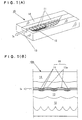
- Fig. 1 one example of the structure of a distributed feedback semiconductor laser 10 as one preferred embodiment of a quantum nano-structure semiconductor laser constructed in accordance with this invention. Basically, the whole structure is manufactured by the method of production disclosed in Japan Patent Application No. 2000-404645 (JP-A 2002-204033).
- an active layer which, as viewed in the direction of light emission Is, comprises a V-groove substrate having a plurality of V-grooves disposed in parallel thereon and limited-length GaAs or InGaAs quantum wires 11 individually formed in V-groove regions of the V-groove substrate and typically measuring 5 to 20 nm in thickness and 10 to 50 nm in the size in the direction of laser beam emission Is and 0.5 to 2 ⁇ m in the size (width) of the direction perpendicular to the direction of laser beam emission Is.
- the pitch of parallel disposition of the plurality of limited-length quantum wires 11 along the direction of laser beam emission Is is set at n ⁇ /4 (wherein n denotes an integer) which is an integer times 1/4 of the wavelength ⁇ in the medium such as, for example, a period of 1/4 or 3/4 wavelength in the medium (0.15 to 0.5 ⁇ m).
- the perimeter of this array of quantum wires is covered with an upper and lower guide layer 13 about 0.2 ⁇ m in a vertical size, a lower AlGaAs clad layer 12 about 1 ⁇ m in thickness and an upper clad layer 1/4.
- One of the upper and lower clad layers 14 and 12 is of an N type and the other layer is of a P type.
- the cross section of these quantum wires 11, as described in Japan Patent Application No. 2000-404645, generally has a falcate shape.
- the clad layers 12 and 14 may be formed of GaAs.
- a group of V-grooves of a limited length is repeatedly formed in the (1-10) direction on a (100) substrate with a period of an integer times of the quarter wavelength in the medium, an N type AlGaAs lower clad layer 12 having an Al percentage of about 0.4 and a non-doped AlGaAs guide layer 13 having an Al percentage of about 0.2, for example, are sequentially formed thereon, further InGaAs quantum wires 11 having an In percentage of about 0.1 is formed, and subsequently a non-dope AlGaAs guide layer 13 having an Al percentage of about 0.2 (since this guide layer, when formed, transforms into an integral member covering the quantum wires 11, the upper and lower guide layers are jointly denoted by a reference numeral 13 in the diagram) and a P type AlGaAs upper clad layer 1/4 having an Al percentage of about 0.4 are continuously grown.
- the laser oscillation is accomplished with a lower threshold than ever because the periodically arrayed quantum wires 11 are closed at both ends thereof and consequently are given a limited length and the diffusion of minority carriers is suppressed in the lateral direction along the quantum wire.
- this achievement has been demonstrated by the present inventors' experiment.
- the existing manufacturing technique has set examples of forming V-grooves in the [01-1] direction by using not only a GaAs (100) substrate but also a GaAs (311)A substrate.
- the present invention can be applied.
- the lower clad layer on the V-groove substrate is allowed to have a decreased thickness and the retention of a periodic structure of V-groove array of a short period is facilitated because the InP substrate is transparent to the oscillation wavelength.
- a structure such as the semiconductor laser 10A of this invention illustrated in Fig. 1(B) is conceivable even though the quantum wires 11 are not formed mutually in a perfectly independent form and individually in a geometric form on the V-groove grating.
- an active layer which appears to be a quantum well layer in the form of a continuous plane, as observed when the opposite sides in the direction of light emission of the parts 11 corresponding to the quantum wires in Fig. 1(A) are connected to the parts 11 of the adjacent quantum wires through a thin active layer part 11a, is enabled to manifest the same function and effect as the semiconductor laser 10 illustrated in Fig. 1(A) so long as the thickness of an active layer 15 is modulated, as illustrated in Fig.
- the same function can be obtained and the oscillation with a low threshold can be achieved even when the width of the waveguide perpendicular to the direction Is of light emission are modulated along the direction Is of light emission in conformity with the period of V-groove grating.
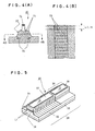
- a semiconductor laser 10B of this invention illustrated in Fig. 2 (A) is such that the part of the active layer 15 serving as an effective oscillating part and having a predetermined width w15 does not jog and constitutes an active layer 15 of the form of a uniform flat plane (sheetlike form).
- the opposite sides thereof form the parts of mountain bases like the bases of a mesa and are furnished with structures each having V-grooves disposed in parallel along the direction Is of light emission with a period of n ⁇ /4, such as 1/4 or 3/4, which is an integer times of the quarter wavelength ⁇ in the medium, namely V-groove gratings.
- Fig. 2(B) which depicts the active layer 15 and the opposite side part 15a thereof exclusively, the opposite mountain base parts 15a continuing to the active layer 15 having the width w15 mentioned above are so shaped as to give rise to grooves 15b corresponding to the V-grooves, while the effective part of the active layer 15 which contributes to the laser oscillation is flat.
- a periodic structure such as of distribution of refractivity in the quantum well layer mentioned above, can be constructed with high accuracy as expected and a low-threshold distributed feedback type semiconductor layer can be likewise obtained even when the edge parts of such an active layer are each provided with a structure of geometrically modulated V-grooves.
- This invention can utilize quantum dots as well.
- the quantum wires 11 depicted as assuming a falcate cross section, depending on the conditions of manufacture may optionally be caused to form a plurality of quantum dots within each of the V-grooves as though they were finely split Naturally, even in this case, the same effect can be expected.
- An artist's concept of this situation is depicted in Fig. 3.
- the quantum wires 11 which are depicted as a physical region continued in the direction of width in the semiconductor laser 10 illustrated in Fig. 1(A) assume a form as though split in the direction of width mentioned above in a semiconductor laser 10C illustrated in Fig. 3 and constitute an aggregate of quantum dots 11' in the individual grooves. Even in this structure, the same function and effect can be manifested as the semiconductor laser of this invention illustrated in Fig. 1(A).
- Fig. 4 illustrates a quantum nano-structure semiconductor laser 20 according to another embodiment of this invention.
- This laser also uses quantum dots 21.
- InGaAs is grown on such a V-groove substrate as described already, with the increased In percent and the thickness of grown film and with a low growth speed, InGaAs or InAs multiple quantum dots 21 can be formed selectively on the V-grooves.
- the intervals between the parallel disposed V-grooves namely the intervals of parallel disposition along the direction of advance of light between the groups of quantum dots 21 arranged in a line, are set similarly to the case of using the quantum wires described above at n ⁇ /4, i.e. an integer times a quarter wavelength in the medium of the laser active layer.
- the shapes of the individual quantum dots 21 are not infrequently dispersed as schematically illustrated in the diagram. And this fact possibly functions rather significantly as described herein below.
- the V-grooves of a limited length do not always retain the shape of grooves incised in the substrate owing to the selective growth. They are allowed to use the shape which results from growing a lower clad layer, forming a guide layer or the like, then withdrawing the substrate once from a growing furnace, incising V-grooves of a limited length thereon, and performing the second growth up to a plurality of repetitions as carried out in the conventional process, such as quantum wires and quantum dots, subsequently forming an upper guide layer and an upper clad layer.
- quantum dots 21 assume a structure such that the entire perimeter of an active layer is encircled with a clad layer of large bandgap energy. Thus, they are equivalent in that buried heterostructures are realized automatically Consequently, the dissipation of injected carriers can be prevented because the electron-hole pairs based on the injection of electric current are retained within quantum dots as schematically shown with a thick arrow mark Ct in Fig. 4 and the diffusion length of minority carriers in the lateral direction along the direction of width schematically indicated with fine arrow marks Ct becomes small.
- Document 4 J. K. Kim, T. A. Strand, R. L. Naone, and L. A.
- the material does not need to be particularly restricted, but is only required to allow realization of a structure contemplated by this invention.
- the InGaAs or InAs quantum dots that are formed by growing InGaAs or InAs to a thickness exceeding the critical film thickness on V-grooves are realistic.
- the V-groove substrate is a GaAs (100) or (311 )A substrate, or an InP (100) or (311)A substrate. This point is held good with the other embodiments of this invention.
- Fig. 5 illustrates another preferred embodiment 30 of the semiconductor laser of this invention.
- a quantum dot laser having quantum dots embedded in an in-plane pattern has been materialized by adopting a technique of crystal growth of the so-called SK mode (refer, for example, to Document 5: Z. Zou, D. L. Huffaker, S. Csutak, and D. G. Deppe, "Ground state lasing from a quantum-dot oxide-confined vertical-cavity surface-emitting laser," Appl. Phys. Letters 75 (1), July 5, 1999, p. 22).
- the etch depth to define the ridge waveguide should be shallow above the active layer for the purpose of avoiding carrier surface recombination on the processing interface.
- This shallow processing layer entails the problem of preventing acquisition of a fully satisfactory stabilization of wavelength.
- this invention allows construction of a DFB type optical resonator even when the quantum dots themselves have random positions by forming a lower clad layer 33 on a V-groove substrate 32, providing an active layer in an upper-lower guide layer 34 with groups of quantum dots 31, thereby forming an upper clad layer 35, and boring the side of a structure confining the quantum dots 31 along the direction of advance of light deep enough to permeate the quantum dots, thereby forming periodic lateral surfaces as exemplified by a quantum nano-structure semiconductor laser 30 illustrated in Fig. 5. That is, this invention allows realization of a DFB laser having a low threshold and enjoying a fully satisfactorily stabilized wavelength without requiring a re-growth process.
- one optical integrated circuit (OEIC) 39 is constructed by integrally forming the part of the semiconductor laser 30 nearly corresponding to the region having formed therein an electrode 37 for a laser, serially with a modulator part 36 corresponding to the region having an electrode 38 for a modulator formed therein.
- the structure of this modulator part 36 per se is not particularly restricted by this invention, but may be a proper known structure selected arbitrarily.
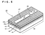
- FIG. 6 is a schematic view of an optical integrated circuit 49 using a two-dimensional photonics crystal and constructed in accordance with this invention.
- This circuit 49 is constructed by forming a lower clad layer 43 on a semiconductor substrate 42, disposing thereon in accordance with this invention as interposed between upper and lower guide layers a multiplicity of groups of quantum dots with a prescribed period, namely a period of an integer times the quarter wavelength in the medium preferably as further superposed in a plurality of layers in the direction of height, forming an upper clad layer 45a and a surface layer 45b, and forming an electrode 47 for a laser in a laser region part 40.
- the embodiment illustrated in Fig. 6 is characterized by having holes 46 bored through a structure having superposed quantum dot layers formed therein along the lateral sides thereof so as to leave behind stripe parts for passing a laser beam in the direction of advance of light and in the vertical direction perpendicular to the lateral direction perpendicular to the direction of advance of light with a prescribed period.
- the period is set, for example, at 1/2 of the wavelength in the medium.
- the stripe parts enclosed with the lines of the holes extending along the direction of advance of light constitute waveguides.
- the intervals of these holes therefore, it is made possible to allow the waveguide wavelength selectivity and enable a signal to be guided through specific waveguides.
- the OEIC 49 necessary for an optical transmission system can be realized by having lasers, modulators, branches, filters, etc. connected onto one and the same substrate through the two-dimensional photonics optical waveguides.
- the modulators provided with the electrodes 48 for modulation are integrated.
- the fact that an active optical module can be realized only by the disposition of holes and electrodes is highly valuable even practically.
- the quantum dots since the surface recombination poses no big problem, a two-dimensional optical circuit can be formed by an additional fabrication.
- the holes 41 may be empty holes filled with air and these empty holes may be optionally filled with a medium of proper refractivity. They are only required to serve as empty holes from the viewpoint of an optical circuit.
- Fig. 7 depicts a monolithic OEIC 50 that makes use of this invention. It has on a proper substrate a ridge type optical waveguide 51 which may be constructed by any of the known techniques. This waveguide 51 has formed therein branch lines that severally serve properly as optical waveguides. These branch lines are each required to have a semiconductor laser of this invention constructed in advance therein as already explained above with reference to Figs. 1 to 3. It is schematically depicted, with a portion magnified for the sake of explanation. The quantum wires 11 already explained and the quantum dots 11', the active layer 15 and the like described above are disposed in the semiconductor laser region 10 (or 10A, 10B, 10C). Thus, the OEIC 50 constitutes a semiconductor laser array.
- the ridge type optical waveguide may be formed after semiconductor laser parts are formed at proper locations preliminarily in the V-groove grating structure under the conditions in conformity to this invention. This invention produces the ease and the convenience with which such structures are formed on V-grooves by one cycle of selective growth.
- each of these waveguides with the structure of an active layer region that is used in the semiconductor laser of this invention as already described with reference to Figs. 3 to 6.
- This invention is enabled by taking into due consideration the same dispositional relation as in the quantum nano-structure semiconductor laser which has been described hitherto concerning the disposition of limited-length quantum wires or quantum dots to provide not only semiconductor lasers but also quantum nano-structure arrays which are applicable to various "optically functional elements.”
- this invention promises useful applications when this invention is defined as a limited-length quantum wire array or a quantum dot array confined in the waveguide region for passing light within the width thereof and parallel disposed in the direction of advance of light with a period of an integer times of the quarter wavelength in the medium of the waveguide.
- the materials and the procedure to be adopted for the manufacture of this array may be the same as those described hitherto regarding the quantum nano-structure semiconductor laser of this invention.
- the quantum nano-structure array contemplated by this invention namely by the structure having limited-length quantum wires or quantum dots disposed with a period conforming to this invention, since the density of states is rendered discrete and the width of gain band is narrowed in the semiconductor laser, the injected carriers are efficiently concentrated on a quantum level conforming to a specific wavelength of oscillation. And this concentration results in decreasing the threshold.
- sharp state density means that the gain is peaked at a sharp wavelength characteristic of the Lorentz type and results in suppressing the change of the peak position thereof.
- the wavelength dependence of refractivity corresponds to the differential waveform.
- the refractivity is nullified in the neighborhood of the center of the gain being oscillated and stable against the variation of carrier concentration.
- change of refractivity against the carrier density is called an "alpha parameter.”
- the active layer formed of the limited-length quantum wire array or quantum dot array disposed in conformity with this invention is capable of appreciably decreasing the alpha parameter and, therefore, is enabled to effect high-speed modulation.
- the mode lock laser and the Mach-Zender type optical switch utilize a supersaturated absorber and the speeds of response of these devices just match the frequency zone necessary for the optical transmission.
- the optical transmission utilizes the pulse transmission in an approximate frequency range of 10 GHz to 100 GHz, which corresponds to the time domain of 10 ps to 100 ps.
- the relevant pulse width just reaches the range of picoseconds because the capture of multiple carriers in the dot level, is slower than the quantum well. If the capture is unduly fast, the number of photons necessary for saturation will be wasted.
- the quantum nano-structure array constructed by this invention can be effectively applied as a frequency modulator/converter.
- the phase relaxing time is called "gamma ( ⁇ )."
- the quantum dots having an isolated quantum state have a longer phase relaxing time and, therefore, manifest the nonlinear effect strongly.
- this invention provides a quantum nano-structure array which has the limited-length quantum wires or quantum dots arranged periodically, it enables the wires or dots to concur on the anti-node of light, causes the aforementioned effect to manifest strongly in a small volume of the active layer, delays the group velocity of light (in other words, reciprocation of light in the material) and allows the gain and absorption of light to occur efficiently.
- the quantum nano-structure array of this invention can serve as an effective device also in constructing various optically functioning elements mentioned above.
- the quantum nano-structure semiconductor lasers and the quantum nano-structure arrays alike which conform to this invention have been delineated as having limited-length quantum wires parallelly disposed, quantum dots formed therein and V-grooves forming an active layer thereon parallel disposed invariably with a period of an integer times of the quarter wavelength in the medium.
- the dispersion of wavelengths can be varied for individual wavelengths depending on the degree of the displacement of the period of quantum wires or V-grooves from 1/4 of the wavelength in the medium, it is made possible by causing numerous longitudinal modes to be propagated invariably at the same speed to induce formation of a state in which numerous wavelengths are synchronized in the same phase (mode lock) or to induce efficient generation of a light pulse of an extremely short (2 - 30 fs) width.
- a semiconductor laser excelling in the property of stabilizing the oscillation frequency with a low threshold preferably by one cycle of selective growth as described above. Since the invention enables limited-length high-density multiple quantum wires and quantum dots to be formed at any necessary positions in the structure of a device, a quantum nano-structure array which promises significant application to highly sophisticated quantum nano-structure semiconductor lasers and various optically functioning elements can be realized by a simple manufacturing process.
- the communication wavelength zone tends to be enlarged in the future and the wavelength zone of 1.0 - 1.6 ⁇ m has been gaining in importance.
- the use of the quantum nano-structure array (limited-length quantum wire array and quantum dot array) provided by this invention allows the wavelength range to be enlarged. Since the array obviates the necessity for re-growth and permits use of a mixed crystal incorporating an Al composition of a large band gap as a clad layer, it is made possible to manufacture a laser not easily affected by the operating temperature (endowed with a high To) and materialize a laser of a stabilized wavelength which is suitably applied to products for general use, such as household appliances and automobiles, which allow rigid control of temperature conditions only with difficulty.
Landscapes
- Physics & Mathematics (AREA)
- Engineering & Computer Science (AREA)
- Chemical & Material Sciences (AREA)
- Optics & Photonics (AREA)
- Nanotechnology (AREA)
- Condensed Matter Physics & Semiconductors (AREA)
- General Physics & Mathematics (AREA)
- Electromagnetism (AREA)
- Crystallography & Structural Chemistry (AREA)
- Theoretical Computer Science (AREA)
- Mathematical Physics (AREA)
- Life Sciences & Earth Sciences (AREA)
- Biophysics (AREA)
- Semiconductor Lasers (AREA)
Abstract
Description
Claims (23)
- A quantum nano-structure semiconductor laser comprising:a grooved semiconductor substrate having a plurality of V-grooves individually extended in directions perpendicular to a direction of advance of an oscillated laser beam and mutually disposed in parallel along the direction of advance of the laser beam; anda plurality of quantum wires formed one on each of the V-grooves by selective growth of a Group III-V compound, said plurality of quantum wires being disposed in parallel along the direction of advance of the laser beam with a period of an integer times of a quarter wavelength in a medium of a laser active layer and individually disposed as an active layer region of a limited length corresponding to a width of stripes of laser.
- A quantum nano-structure semiconductor laser according to claim 1, wherein a waveguide mode is stabilized by intentionally displacing a period of parallel disposition from said period of an integer times 1/4 instead of disposing said plurality of quantum wires in parallel along said direction of advance of the laser beam with a period of an integer times of the quarter wavelength in the medium of the laser active layer for a broadband wavelength oscillation or short pulse oscillation in a state of mode lock is materialized by promoting compensation of dispersion between oscillation modes.
- A quantum nano-structure semiconductor laser according to claim 1 or claim 2, wherein said substrate is a GaAs (100) or (311)A substrate; said V-grooves are limited-length V-grooves formed in a [01-1] direction on the GaAs (100) or (311)A substrate; said quantum wires are limited-length wires manufactured from GaAs or InGaAs and grown on said limited-length V-grooves; and said quantum wires are individually furnished with GaAs or AlGaAs clad regions adapted to cover said quantum wires.
- A quantum nano-structure semiconductor laser according to claim 1 or claim 2, wherein said substrate is an InP (100) or (311)A substrate; said V-grooves are limited-length V-grooves formed in a [01-1] direction on the InP (100) or (311)A substrate; said quantum wires are limited-length wires manufactured from InGaAs and grown on said limited-length V-grooves, and said quantum wires are furnished with InAlAs clad areas adapted to cover said quantum wires.
- A quantum nano-structure semiconductor laser comprising:a grooved semiconductor substrate having a plurality of V-grooves individually extended in directions perpendicular to a direction of advance of an oscillated laser beam and mutually disposed in parallel along said direction of advance of the laser beam, a period for parallel disposition of said plurality of V-grooves being a period of an integer times of a quarter wavelength in a medium of a laser active layer; andactive layers formed on said V-grooves by selective growth of a Group III-V compound and having a thickness or width thereof modulated in accordance with said period of said V-grooves.
- A quantum nano-structure semiconductor laser according to claim 5, wherein a waveguide mode is stabilized by intentionally displacing said period for parallel disposition from said period of an integer times 1/4 instead of disposing said plurality of quantum wires in parallel along said direction of advance of the laser beam with a period of an integer times of the quarter wavelength in the medium of the laser active layer for a broad band wavelength oscillation or short pulse oscillation in a state of mode lock is materialized by promoting compensation of dispersion between oscillation modes.
- A quantum nano-structure semiconductor laser according to claim 5 or claim 6, wherein said substrate is a GaAs (100) or (311)A substrate; said V-grooves are limited-length V-grooves formed in a [01-1] direction on the GaAs (100) or (311)A substrate; said laser active layer is manufactured from GaAs or InGaAs and grown on said limited-length V-grooves; and said active layers are furnished with clad regions of GaAs or AlGaAs adapted to cover said active layers.
- A quantum nano-structure semiconductor laser according to claim 5 or claim 6, wherein said substrate is an InP (100) or (311)A substrate; said V-grooves are limited-length V-grooves formed in a [01-1] direction on the InP (100) or (311)A substrate; said active layers are manufactured from InGaAs and grown on said limited-length V-grooves; and said active layers are furnished with clad regions of InAlAs adapted to cover said active layers.
- A quantum nano-structure semiconductor laser comprising:a laser active layer of a prescribed width formed on a semiconductor substrate by selective growth of a Group III-V compound, serving as an effective laser oscillating part, and assuming a flat sheet form; andV-grooves provided on opposite lateral parts continuing into the laser active layer in a direction of width perpendicular to a direction of advance of an oscillated laser beam, individually extended in directions perpendicular to said direction of advance of the laser beam and mutually disposed in parallel along said direction of advance of the laser beam with a period of an integer times of a quarter wavelength in a medium of said laser active layer.
- A quantum nano-structure semiconductor laser according to claim 9, wherein a waveguide mode is stabilized by intentionally displacing said period of parallel disposition from said period of an integer times 1/4 instead of disposing said plurality of quantum wires in parallel along said direction of advance of the laser beam with a period of an integer times of the quarter wavelength in the medium of the laser active layer, for a broad band wavelength oscillation or short pulse oscillation in a state of mode lock is materialized by promoting compensation of dispersion between oscillation modes.
- A quantum nano-structure semiconductor laser according to any one of claim 1 to claim 10, wherein said semiconductor laser is used as a gain-coupled or refractivity-coupled distribution feedback laser.
- A quantum nano-structure semiconductor laser comprising:a grooved Group III-V compound semiconductor substrate having a plurality of V-grooves individually extended in directions perpendicular to a direction of advance of an oscillated laser beam and mutually disposed in parallel along said direction of advance of the laser beam with a period of an integer times of a quarter wavelength in a medium of a laser active layer;a plurality of InGaAs or InAs quantum dots formed one in each of base parts of said V-grooves by growing InGaAs or InAs on said V-grooves to not less than a critical film thickness, said plurality of quantum dots serving as laser active regions; andGaAs or AlGaAs layers on said laser active regions serving as clad regions.
- A quantum nano-structure semiconductor laser according to claim 12, wherein a waveguide mode is stabilized by intentionally displacing said period of parallel disposition from said period of an integer times 1/4 instead of disposing the period of parallel disposition of said plurality of V-grooves at an integer times of the quarter wavelength in the medium of said laser active layer, for a broadband wavelength oscillation or short pulse oscillation in a state of mode lock is materialized by promoting compensation for dispersion between oscillation modes
- A quantum nano-structure semiconductor laser according to claim 12 or claim 13, wherein said grooved Group III-V compound substrate is a GaAs (100) or (311)A substrate or an InP (100) or (311)A substsrate.
- A quantum nano-structure semiconductor laser according to claim 12 or claim 13, wherein a structure having said quantum dots formed therein is mesa-etched to be transformed into a distributed feedback laser.
- A quantum nano-structure semiconductor laser according to claim 12 or claim 13, wherein a structure having said quantum dots formed therein has lateral surfaces along said direction of the laser beam imparted with corrugations to be transformed into a distributed feedback laser.
- A quantum nano-structure semiconductor layer according to claim 12 or claim 13, wherein a structure having said quantum dots formed therein has a plurality of through holes bored therein with a prescribed period along lateral sides leaving behind stripe parts for passing light and along vertical directions individually perpendicular to both said direction of advance of the laser beam and a lateral direction perpendicular thereto.
- A quantum nano-structure semiconductor laser according to claim 17, wherein said period is ½ of the wavelength in the medium.
- An array of quantum nano-structure semiconductor lasers, comprising a substrate, a plurality of quantum nano-structure semiconductor lasers set forth in any one of claim 1 to claim 18 disposed in parallel on the substrate and a ridge type waveguide that connects the semiconductor lasers to give rise to an array structure.
- A quantum nano-structure array comprising:a grooved semiconductor substrate having a plurality of V-grooves individually extended in directions perpendicular to a direction of advance of a passing light and mutually disposed in parallel along said direction of advance of the light; anda plurality of quantum wires grown one on each of the V-grooves of said grooved semiconductor substrate by selective growth of a Group III-V compound, mutually disposed in parallel along said direction of advance of the light with a period of an integer times of a quarter wavelength in a medium of a waveguide layer for passing light and intended to serve as limited-length waveguide regions corresponding to a width of the waveguide layer.
- A quantum nano-structure array according to claim 20, wherein a waveguide mode is stabilized, or dispersion regarding passing light is compensated by intentionally displacing said period of parallel disposition from said period of an integer times 1/4 instead of disposing said plurality of quantum wires in parallel along said direction of advance of the light with a period of an integer times of the quarter wavelength in the medium of the waveguide layer.
- A quantum nano-structure array comprising:a grooved semiconductor substrate having a plurality of V-grooves individually extended in directions perpendicular to a direction of advance of a passing light and mutually disposed in parallel along said direction of advance of the light with a period of an integer times of a quarter wavelength in a medium of a waveguide layer;a plurality of InGaAs or InAs quantum dots formed one in each of base parts of said V-grooves by growing InGaAs or InAs on said V-grooves to not less than a critical film thickness, said plurality of quantum dots serving as laser active regions; andGaAs or AlGaAs layers formed on the quantum dots for serving as clad regions.
- A quantum nano-structure array according to claim 22, wherein a waveguide mode is stabilized, or dispersion regarding a passing light is compensated by intentionally displacing said period of parallel disposition from said period of an integer times 1/4 instead of setting the period of parallel disposition of said plurality of V-grooves at an integer times of the quarter wavelength in the medium of said waveguide layer.
Applications Claiming Priority (3)
| Application Number | Priority Date | Filing Date | Title |
|---|---|---|---|
| JP2002051548 | 2002-02-27 | ||
| JP2002051548 | 2002-02-27 | ||
| PCT/JP2003/001975 WO2003073570A1 (en) | 2002-02-27 | 2003-02-24 | Quantum nano-composite semiconductor laser and quantum nano-composite array |
Publications (3)
| Publication Number | Publication Date |
|---|---|
| EP1480304A1 true EP1480304A1 (en) | 2004-11-24 |
| EP1480304A4 EP1480304A4 (en) | 2005-12-28 |
| EP1480304B1 EP1480304B1 (en) | 2007-04-11 |
Family
ID=27764312
Family Applications (1)
| Application Number | Title | Priority Date | Filing Date |
|---|---|---|---|
| EP03707006A Expired - Lifetime EP1480304B1 (en) | 2002-02-27 | 2003-02-24 | Quantum nano-composite semiconductor laser and quantum nano-composite array |
Country Status (7)
| Country | Link |
|---|---|
| US (1) | US7463661B2 (en) |
| EP (1) | EP1480304B1 (en) |
| JP (1) | JP4345483B2 (en) |
| KR (1) | KR100967977B1 (en) |
| CA (1) | CA2477610C (en) |
| DE (1) | DE60313140T2 (en) |
| WO (1) | WO2003073570A1 (en) |
Cited By (2)
| Publication number | Priority date | Publication date | Assignee | Title |
|---|---|---|---|---|
| WO2005112210A1 (en) * | 2004-05-14 | 2005-11-24 | Bookham Technology Plc | Semiconductor devices including gratings formed using quantum dots and method of manufacture |
| CN117268279A (en) * | 2023-09-13 | 2023-12-22 | 北京讯腾智慧科技股份有限公司 | Strain optical fiber sensor, manufacturing method thereof and integrated waveguide sensor |
Families Citing this family (18)
| Publication number | Priority date | Publication date | Assignee | Title |
|---|---|---|---|---|
| JP4613304B2 (en) * | 2004-09-07 | 2011-01-19 | 独立行政法人産業技術総合研究所 | Quantum nanostructured semiconductor laser |
| US20060120428A1 (en) * | 2004-12-08 | 2006-06-08 | Dae Kon Oh | Distributed feedback (DFB) semiconductor laser and fabrication method thereof |
| KR100794653B1 (en) * | 2005-12-06 | 2008-01-14 | 한국전자통신연구원 | Distributed Feedback Quantum Dot Semiconductor Laser Structure |
| US20080009844A1 (en) * | 2006-06-26 | 2008-01-10 | Ingeborg Rolle | Device for Laser Surgery |
| JP2010258088A (en) * | 2009-04-22 | 2010-11-11 | Qd Laser Inc | Laser system |
| US8076217B2 (en) | 2009-05-04 | 2011-12-13 | Empire Technology Development Llc | Controlled quantum dot growth |
| JP2011044539A (en) * | 2009-08-20 | 2011-03-03 | Qd Laser Inc | Semiconductor laser and method for manufacturing the same, optical module, and optical transmission system |
| US9057891B2 (en) * | 2009-09-11 | 2015-06-16 | The United States Of America, As Represented By The Secretary Of The Navy | Nonlinear frequency conversion in nanoslab optical waveguides |
| WO2011133144A1 (en) | 2010-04-20 | 2011-10-27 | Hewlett-Packard Development Company, L.P. | A self-arranging, luminescence-enhancement device for surface-enhanced luminescence |
| US9001324B2 (en) | 2010-07-30 | 2015-04-07 | Hewlett-Packard Development Company, L.P. | Optical fiber surface enhanced raman spectroscopy (SERS) probe |
| WO2012075461A1 (en) * | 2010-12-02 | 2012-06-07 | Nanocrystal Corporation | Defect-free group iii - nitride nanostructures and devices based on repetitive multiple step growth-etch sequence |
| US8593629B2 (en) * | 2011-02-17 | 2013-11-26 | Hewlett-Packard Development Company, L.P. | Apparatus for performing SERS |
| US9377409B2 (en) | 2011-07-29 | 2016-06-28 | Hewlett-Packard Development Company, L.P. | Fabricating an apparatus for use in a sensing application |
| CN102684068B (en) * | 2012-05-28 | 2014-04-23 | 西安交通大学 | Tunable laser based on nanowire array and preparation process thereof |
| JP6274224B2 (en) * | 2014-01-10 | 2018-02-07 | 富士通株式会社 | Optical semiconductor device and manufacturing method thereof |
| DE102014106209B3 (en) | 2014-05-05 | 2015-08-27 | Nanoplus Nanosystems And Technologies Gmbh | Interband cascade laser and method for producing an inter-band cascade laser comprising a feedback element |
| WO2018185829A1 (en) * | 2017-04-04 | 2018-10-11 | 三菱電機株式会社 | Semiconductor device, and method for manufacturing semiconductor device |
| WO2024172821A2 (en) * | 2022-02-22 | 2024-08-22 | University Of Southern California | On-chip integrable ordered and highly spectrally uniform single photon sources for scalable quantum optical circuits |
Family Cites Families (24)
| Publication number | Priority date | Publication date | Assignee | Title |
|---|---|---|---|---|
| US4302729A (en) * | 1979-05-15 | 1981-11-24 | Xerox Corporation | Channeled substrate laser with distributed feedback |
| JPS5948975A (en) * | 1982-09-14 | 1984-03-21 | Nec Corp | Semiconductor light emitting element |
| JPH07109928B2 (en) * | 1989-06-30 | 1995-11-22 | 光計測技術開発株式会社 | Semiconductor laser device and manufacturing method thereof |
| JP2957198B2 (en) * | 1989-07-18 | 1999-10-04 | 光計測技術開発株式会社 | Semiconductor laser device |
| DE69027368T2 (en) * | 1989-06-30 | 1997-01-30 | Optical Measurement Technology | Semiconductor laser and method of manufacturing the same |
| JPH05145169A (en) * | 1990-09-05 | 1993-06-11 | Hikari Keisoku Gijutsu Kaihatsu Kk | Semiconductor distributed feedback laser apparatus |
| US5114877A (en) * | 1991-01-08 | 1992-05-19 | Xerox Corporation | Method of fabricating quantum wire semiconductor laser via photo induced evaporation enhancement during in situ epitaxial growth |
| EP0553994A1 (en) * | 1992-01-29 | 1993-08-04 | AT&T Corp. | Compact optical pulse source |
| US5305336A (en) * | 1992-01-29 | 1994-04-19 | At&T Bell Laboratories | Compact optical pulse source |
| US5449247A (en) * | 1992-08-27 | 1995-09-12 | Smith; Delbert G. | Boat mooring station |
| JP2767676B2 (en) * | 1993-03-19 | 1998-06-18 | 松下電器産業株式会社 | Method for forming fine structure of compound semiconductor |
| US5529952A (en) * | 1994-09-20 | 1996-06-25 | Texas Instruments Incorporated | Method of fabricating lateral resonant tunneling structure |
| US5749313A (en) * | 1996-02-06 | 1998-05-12 | Shackelford, Jr.; Francis H. | Watercraft lift |
| US5917194A (en) * | 1996-07-17 | 1999-06-29 | The United States Of America As Represented By The Secretary Of The Army | Mesoscopic electronic devices with tailored energy loss scattering |
| US5888019A (en) * | 1997-08-25 | 1999-03-30 | Quastad; Donald D. | Walking hoist |
| TW388144B (en) * | 1997-09-30 | 2000-04-21 | Mitsui Chemicals Inc | Semiconductor laser device |
| JP3875799B2 (en) * | 1997-09-30 | 2007-01-31 | 三井化学株式会社 | Semiconductor laser device |
| JP4375834B2 (en) * | 1998-03-19 | 2009-12-02 | シャープ株式会社 | Gain-coupled distributed feedback semiconductor laser device and manufacturing method thereof |
| JPH11330619A (en) * | 1998-05-18 | 1999-11-30 | Nippon Telegr & Teleph Corp <Ntt> | Optical device |
| JP2000124441A (en) * | 1998-10-13 | 2000-04-28 | Fujitsu Ltd | Fabrication method of semiconductor quantum dot device |
| JP3338869B2 (en) * | 1999-06-09 | 2002-10-28 | 独立行政法人産業技術総合研究所 | Method for optimizing refractive index distribution of dispersion compensating mirror, dispersion compensating mirror manufactured based on the method, and its application device |
| JP4008180B2 (en) * | 2000-03-29 | 2007-11-14 | パイオニア株式会社 | Distributed feedback ridge type semiconductor laser |
| JP3849115B2 (en) * | 2000-05-15 | 2006-11-22 | 富士通株式会社 | Semiconductor laser device |
| JP3536978B2 (en) | 2000-12-27 | 2004-06-14 | 独立行政法人産業技術総合研究所 | Method of forming quantum wire or quantum well layer, and distributed feedback semiconductor laser using quantum wire or quantum well layer formed by the method |
-
2003
- 2003-02-24 EP EP03707006A patent/EP1480304B1/en not_active Expired - Lifetime
- 2003-02-24 DE DE60313140T patent/DE60313140T2/en not_active Expired - Lifetime
- 2003-02-24 US US10/505,770 patent/US7463661B2/en not_active Expired - Fee Related
- 2003-02-24 KR KR1020047013359A patent/KR100967977B1/en not_active Expired - Fee Related
- 2003-02-24 WO PCT/JP2003/001975 patent/WO2003073570A1/en not_active Ceased
- 2003-02-24 JP JP2003572142A patent/JP4345483B2/en not_active Expired - Lifetime
- 2003-02-24 CA CA2477610A patent/CA2477610C/en not_active Expired - Fee Related
Cited By (3)
| Publication number | Priority date | Publication date | Assignee | Title |
|---|---|---|---|---|
| WO2005112210A1 (en) * | 2004-05-14 | 2005-11-24 | Bookham Technology Plc | Semiconductor devices including gratings formed using quantum dots and method of manufacture |
| CN117268279A (en) * | 2023-09-13 | 2023-12-22 | 北京讯腾智慧科技股份有限公司 | Strain optical fiber sensor, manufacturing method thereof and integrated waveguide sensor |
| CN117268279B (en) * | 2023-09-13 | 2024-05-10 | 北京讯腾智慧科技股份有限公司 | Strain optical fiber sensor, manufacturing method thereof and integrated waveguide sensor |
Also Published As
| Publication number | Publication date |
|---|---|
| CA2477610C (en) | 2010-12-07 |
| WO2003073570A1 (en) | 2003-09-04 |
| CA2477610A1 (en) | 2003-09-04 |
| DE60313140T2 (en) | 2007-07-19 |
| US7463661B2 (en) | 2008-12-09 |
| US20060056472A1 (en) | 2006-03-16 |
| EP1480304A4 (en) | 2005-12-28 |
| JPWO2003073570A1 (en) | 2005-06-23 |
| JP4345483B2 (en) | 2009-10-14 |
| EP1480304B1 (en) | 2007-04-11 |
| DE60313140D1 (en) | 2007-05-24 |
| KR20040102018A (en) | 2004-12-03 |
| KR100967977B1 (en) | 2010-07-07 |
Similar Documents
| Publication | Publication Date | Title |
|---|---|---|
| US7463661B2 (en) | Quantum nano-structure semiconductor laser | |
| CA2424468C (en) | Quantum dash devices | |
| US6816525B2 (en) | Quantum dot lasers | |
| CN105164874B (en) | Multi-wavelength quantum cascade laser by growing different active and passive core layers | |
| JP2007318165A (en) | Quantum dot laser | |
| CN1701476A (en) | Semiconductor laser based on the effect of photonic band gap crystal-mediated filtration of higher modes of laser radiation and method of making same | |
| JP2558744B2 (en) | Semiconductor laser device and manufacturing method thereof | |
| EP1952495B1 (en) | Method and structure of germanium laser on silicon | |
| US4922500A (en) | Cross-coupled quantum-well stripe laser array | |
| Razeghi et al. | Low-threshold distributed feedback lasers fabricated on material grown completely by LP-MOCVD | |
| Kapon et al. | Patterned quantum well semiconductor laser arrays | |
| Ledentsov et al. | Novel approaches to semiconductor lasers | |
| Cheng | Heterostructure Photonic Devices | |
| Nishi | Device applications of quantum dots | |
| Joyner | Advances in Semiconductor Laser Growth and Fabrication Technology | |
| Ustinov et al. | Semiconductor quantum dot lasers | |
| Shiau et al. | Strained quantum-well leaky-mode diode laser arrays | |
| Dragoman et al. | Devices for Coherent Light Generation | |
| Kapon | Quantum wires and quantum dots for optoelectronics: Recent advances with epitaxial growth on nonplanar substrates | |
| WO2006088293A1 (en) | Quantum well laser diode having wide band gain | |
| Yu et al. | Disordering of InGaAs/GaAs multiquantum well structure by impurity-free vacancy diffusion for advanced optoelectronic devices and their integration | |
| JP2005512321A (en) | Method for manufacturing integrated semiconductor components on a semiconductor substrate |
Legal Events
| Date | Code | Title | Description |
|---|---|---|---|
| PUAI | Public reference made under article 153(3) epc to a published international application that has entered the european phase |
Free format text: ORIGINAL CODE: 0009012 |
|
| 17P | Request for examination filed |
Effective date: 20040830 |
|
| AK | Designated contracting states |
Kind code of ref document: A1 Designated state(s): AT BE BG CH CY CZ DE DK EE ES FI FR GB GR HU IE IT LI LU MC NL PT SE SI SK TR |
|
| RAP1 | Party data changed (applicant data changed or rights of an application transferred) |
Owner name: NATIONAL INSTITUTE OF ADVANCED INDUSTRIAL SCIENCE Owner name: JAPAN SCIENCE AND TECHNOLOGY AGENCY |
|
| RAP1 | Party data changed (applicant data changed or rights of an application transferred) |
Owner name: JAPAN SCIENCE AND TECHNOLOGY AGENCY |
|
| RIC1 | Information provided on ipc code assigned before grant |
Ipc: 7H 01L 29/06 B Ipc: 7H 01S 5/12 A |
|
| A4 | Supplementary search report drawn up and despatched |
Effective date: 20051114 |
|
| GRAP | Despatch of communication of intention to grant a patent |
Free format text: ORIGINAL CODE: EPIDOSNIGR1 |
|
| RIC1 | Information provided on ipc code assigned before grant |
Ipc: H01L 29/06 20060101ALI20060906BHEP Ipc: H01S 5/34 20060101AFI20060906BHEP |
|
| GRAS | Grant fee paid |
Free format text: ORIGINAL CODE: EPIDOSNIGR3 |
|
| GRAA | (expected) grant |
Free format text: ORIGINAL CODE: 0009210 |
|
| AK | Designated contracting states |
Kind code of ref document: B1 Designated state(s): DE FR GB |
|
| REG | Reference to a national code |
Ref country code: GB Ref legal event code: FG4D |
|
| REF | Corresponds to: |
Ref document number: 60313140 Country of ref document: DE Date of ref document: 20070524 Kind code of ref document: P |
|
| PLBE | No opposition filed within time limit |
Free format text: ORIGINAL CODE: 0009261 |
|
| STAA | Information on the status of an ep patent application or granted ep patent |
Free format text: STATUS: NO OPPOSITION FILED WITHIN TIME LIMIT |
|
| 26N | No opposition filed |
Effective date: 20080114 |
|
| PGFP | Annual fee paid to national office [announced via postgrant information from national office to epo] |
Ref country code: FR Payment date: 20100311 Year of fee payment: 8 |
|
| PGFP | Annual fee paid to national office [announced via postgrant information from national office to epo] |
Ref country code: GB Payment date: 20100226 Year of fee payment: 8 |
|
| PGFP | Annual fee paid to national office [announced via postgrant information from national office to epo] |
Ref country code: DE Payment date: 20100409 Year of fee payment: 8 |
|
| GBPC | Gb: european patent ceased through non-payment of renewal fee |
Effective date: 20110224 |
|
| REG | Reference to a national code |
Ref country code: FR Ref legal event code: ST Effective date: 20111102 |
|
| REG | Reference to a national code |
Ref country code: DE Ref legal event code: R119 Ref document number: 60313140 Country of ref document: DE Effective date: 20110901 |
|
| PG25 | Lapsed in a contracting state [announced via postgrant information from national office to epo] |
Ref country code: FR Free format text: LAPSE BECAUSE OF NON-PAYMENT OF DUE FEES Effective date: 20110228 |
|
| PG25 | Lapsed in a contracting state [announced via postgrant information from national office to epo] |
Ref country code: GB Free format text: LAPSE BECAUSE OF NON-PAYMENT OF DUE FEES Effective date: 20110224 |
|
| PG25 | Lapsed in a contracting state [announced via postgrant information from national office to epo] |
Ref country code: DE Free format text: LAPSE BECAUSE OF NON-PAYMENT OF DUE FEES Effective date: 20110901 |