TECHNICAL FIELD
The present invention relates to an exposure apparatus
and exposure method used when producing a semiconductor
integrated circuit, a liquid crystal display, a thin film
magnetic head, or another microdevice or a photomask by
photolithography.
BACKGROUND ART
In photolithography, one step in the production of a
microdevice, use is made of an exposure apparatus for
projection exposure of images of patterns of a photomask or
reticle (hereinafter referred to generally as a "reticle")
on to a substrate for exposure (semiconductor wafer or glass
plate coated with a photoresist, light-transparent substrate
called a "blank", etc.) In recent years, to deal with the
increasingly large size of the exposure area accompanying the
increased size of substrates, a stitching type exposure
apparatus which partitions the exposure area of the substrate
into a plurality of unit areas (hereinafter sometimes referred
to as "shots" or "shot areas") and successively projects and
exposes images of corresponding patterns on the shots has been
developed.
In such an exposure apparatus, there was sometimes
misalignment in stitched portions of shots due to aberration
of the projection optical system, positioning error of the
reticle or substrate, etc. Therefore, parts of the image of
the patterns for one shot were superposed over parts of the
images of the patterns for other shots adjoining it in the
exposure. At an overlay parts of images of patterns, the
exposure becomes greater than parts other than overlay parts,
so for example the line width (width of lines or spaces) at
overlay parts of patterns formed on the substrate becomes
thinner or thicker in accordance with characteristics of the
photoresist.
Therefore, the profile of exposure at parts forming
overlay parts of the shots is set to a slant so as to become
smaller the further toward the outside and the overall amount
of exposure of overlay parts is made equal to the exposure
of parts other than overlay parts by two exposures so as prevent
changes in line width at these overlay parts.
As a technique for realizing a slanted profile of
exposure at overlay parts of shots, it is known to form
light-attenuating parts limiting in a slanting fashion the
amount of light transmittance at portions of the reticle itself
corresponding to overlay parts. Due to the formation of the
light-attenuating parts in the reticle itself, however, the
steps and cost of the manufacturing process of the reticle
increase and the cost of manufacturing the microdevice etc.
increase. Therefore, an exposure apparatus is being developed
which is provided with a density filter formed with
light-attenuating parts similar to the above on a glass plate
at positions substantially conjugate with the pattern
formation surface of the reticle or which is provided with
a blind mechanism having light-blocking plates (blinds) able
to advance into or retract from the optical path at positions
substantially conjugate with the pattern formation surface
of the reticle and realizes a slanted profile of exposure by
making the light-blocking plates advance or retract during
the exposure of the substrate.
When using the above-mentioned exposure apparatus to
transfer the patterns of a reticle to a substrate, however,
it is required that the pattern density dependency of ΔCD (OPE
characteristic: optical proximity effect) be small. Here,
"ΔCD" means the amount of deviation of the patterns to be formed
on the substrate with respect to the target line width (line
width error). The "OPE characteristic" means the
characteristic of change of the ΔCD, even when the line widths
of the patterns on the reticle are the same, depending on whether
the patterns are isolated patterns or dense patterns and also
whether they are lines or spaces. Further, the degree of change
of the ΔCD does not only depend on the density of the patterns
and is known to also dependon the wavelength of the illumination
light irradiated on the reticle, the numerical aperture (NA)
of the projection optical system, the pattern size, the
illumination σ (σ value = emission side numerical aperture
of illumination system/incident side numerical aperture of
projection optical system), etc.
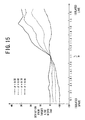
Here, an example of the OPE characteristic of an exposure
apparatus provided with a KrF excimer laser (wavelength: 248
nm) light source and provided with a 0.75 numerical aperture
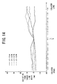
projection optical system will be explained. FIG. 14 is a view
of theOPE characteristic when changing the density of patterns
with a pattern size of 360 nm and illumination σ. FIG. 15 is
a view of the OPE characteristic when changing the density
of patterns with a pattern size of 200 nm and illumination
σ. The "pattern size" spoken of here is the size (line width)
of the patterns on the substrate. In FIG. 14 and FIG. 15, the
abscissa gives the ratio of the lines and spaces and the ordinate
gives the amount of deviation (ΔCD) from the target line width.
Referring to FIG. 14, it will be understood that when
the pattern size is 360 nm, the amount of deviation from the
target line width when changing the ratio of lines and spaces
tends to deteriorate as the patterns become isolated lines
except when setting the illumination σ to 0.55. Further, from
the results of FIG. 14, it will be understood that when setting
the illumination a to 0.55, the extent of the amount of deviation
from the target line width when changing the density of the
patterns (extent of ΔCD) becomes the minimum, so the optimal
illumination σ for the pattern size (360 nm) is 0.55.
Next, referring to FIG. 15, it will be understood that
when the pattern size is 200 nm, the amount of deviation from
the target line width when changing the ratio of lines and
spaces tends to deteriorate as the patterns become isolated
lines regardless of the setting of the illumination σ. Further,
in the results shown in FIG. 15, the extent of the amount of
deviation from the target line width (extent of ΔCD) when
changing the density of the patterns becomes the minimum when
setting the illumination σ to 0.85, so it will be understood
that the illumination σ optimal for the pattern size (200 nm)
is 0.85. From the above, to improve the OPE characteristic
(pattern density dependency of ΔCD), it is necessary to set
the optimal illumination σ for each pattern size.
However, if for example changing the illumination σ for
each pattern size of the patterns for transfer in order to
improve the above OPE characteristic, the widths of the overlay
parts of the shots explained above will end up changing. The
reason is that when using a density filter having
light-attenuating parts changing the probability of presence
of fine dots for example in order to obtain a slanted profile
of exposure at the overlay parts of the shots, sometimes the
fine dots are prevented from being resolved by arranging the
density filter off from the conjugate plane of the pattern
forming surface of the reticle. At the time of such an
arrangement, if changing the illumination σ, the incident angle
of the light rays on the density filter will end up changing
and as a result the width of the overlay parts of the shots
will change.
FIG. 16 is a view of the changes in the profile of exposure
when changing the illumination σ, while FIG. 17 is a view of
the amount of exposure at the overlay parts when changing the
illumination σ. In FIG. 16 and FIG. 17, PR0 is the profile
of exposure when setting the illumination σ at the standard
value. Further, W is the width of an exposure area (width of
transfer of patterns) when setting the illumination σ at the
standardvalue, whileWO is the width of an overlay part. Further,
PR1 is the profile of exposure when reducing the illumination
σ, while PR2 is the profile of exposure when increasing the
illumination σ.
As will be understood from FIG. 16 and FIG. 17, if reducing
the illumination σ, the width of an overlay part changes by
being reduced from W0 to W1 and the gradient of the amount
of exposure at the overlay part becomes sharp. Therefore, if
even a slight offset in position of the shots occurs, the amount
of exposure of the overlay part for the offset will change
greatly and as a result the change in line width will become
sensitive to the offset. Conversely, if increasing the
illumination σ, the width of the overlay part will change by
being enlarged from W0 to W2 and the gradient of the amount
of exposure at the overlay part will become gentler, so the
change of the amount of exposure of the overlay part for offset
of the shots will become smaller. However, part of the overlay
part will be enlarged outside of the exposure area and that
part outside of the exposure area will end up being blocked
by a light-blocking strip formed at the reticle.
As shown in FIG. 17, when setting the illumination σ
at the standard value, the combined amount of exposure PR10
at the overlay part W0 will become the same as the amount of
exposure outside of the overlay part. Even if the illumination
σ is reduced, the combined amount of exposure PR11 at the overlay
part W1 will become the same as the amount of exposure outside
of the overlay part W2. However, if increasing the illumination
σ, locations will arise (locations shown by the symbol Q in
FIG. 17) where the combined amount of exposure PR12 in the
overlay part W2 differs from the amount of exposure outside
the overlay part, so the line width will change in the overlay
part W2.
In this way, in the past, there was the problem that
if for example changing the illumination σ or other
illumination conditions to improve the OPE characteristic,
the amount of change in the combined amount of exposure of
an overlay part with respect to offset of the shots became
greater and there was a susceptibility to changes in line width
and also locations arose where the combined amount of exposure
in the overlay part became insufficient and changes in line
width occurred in the overlay part.
DISCLOSURE OF THE INVENTION
The present invention was made in consideration of these
problems in the prior art and has as its object to provide
an exposure apparatus and an exposure method enabling the
formation of fine patterns of the targeted line widths with
a high accuracy (fidelity) without the amount of exposure at
an overlay part becoming insufficient and without the
occurrence of a change in the amount of exposure at an overlay
part sensitive to positional error of the shots even when
changing the illumination conditions.
In the explanation given in this section, the invention
will be explained corresponding to part notations shown in
the drawings expressing the embodiments, but the requirements
of the present invention are not limited to the members shown
in the drawings given these part notations.
According to a first aspect of the present invention,
there is provided an exposure apparatus which irradiates a
plurality of areas where peripheral parts partially overlap
on a sensitive object (4) by an energy beam (IL) through patterns,
provided with a setting device (Fj, BL) for setting cumulative
amounts of energy at the peripheral parts due to the irradiation
by the energy beam to become a gradually decreasing slanted
profile and a correction device (9, DR1) for correcting changes
in widths of peripheral parts arising along with a change in
the illumination conditions of the patterns.
If changing the illumination conditions, as explained
above, the widths of the peripheral parts where the cumulative
amount of energy is set at a slant change and the cumulative
amounts of energy at the overlay parts where the peripheral
parts overlap with other peripheral parts adjoining them will
not become the desired value. As opposed to this, in the present
invention, even if the illumination conditions are changed,
the widths of the peripheral parts are kept from changing by
correction by the correction device, so even if changing the
illumination conditions, the widths of the overlay parts can
be set to the desired value. Therefore, there will no longer
be cases where the cumulative amount of energy becomes
partially insufficient in an overlay part or the amount of
energy at an overlay part changes sensitively with respect
to positional error of the areas where the patterns are
transferred and the cumulative amounts of energy at the overlay
parts can be uniformly set to the desired value. As a result,
it is possible to form fine patterns of the targeted line widths
with a high accuracy and fidelity.
The setting device is not particularly limited, but it
is possible to employ one including a density filter (Fj) having
a light-attenuating part for gradually reducing the passed
amount of energy of the parts of the energy beam corresponding
to the peripheral parts or a blind mechanism (BL) having light
attenuating plates (127A to 127D) for entering into and
retracting from the irradiation of the energy beam at the parts
of the energy beam corresponding to the peripheral parts. Note
that this setting device is preferably arranged near the
patterns or near a plane conjugate optically with the patterns.
The setting device may include a position adjustment
device (DR1) for adjusting the position of the density filter
or blind mechanism in the direction along the path (AX) of
the energy beam. In this case, by moving the density filter
or blind mechanism in a direction along the path of the energy
beam in accordance with a change in the illumination conditions,
it is possible to adjust the widths of the overlay parts. Further,
it is possible to adjust the widths of the peripheral parts
by moving the blind mechanism in a direction perpendicular
to the path (AX) of the energy beam.
As the setting device, it is possible to employ one
including a plurality of density filters differing in widths
of the light-attenuating parts. In this case, it is possible
to correct the widths of the peripheral parts by changing the
density filter positioned on the path of the energy beam with
a density filter able to correct changes in the widths of the
peripheral parts in accordance with a change in the
illumination conditions.
The correction device may correct the widths of the
peripheral parts without changing the position of the setting
device or, along with this, adjusting the optical
characteristics of the optical elements (113, 114, 116)
arranged on the path of the energy beam from the setting device
to the patterns.
When the overlay parts where peripheral parts overlap
and parts other than the overlay parts differ in cumulative
amounts of energy along with correction of the widths of the
peripheral parts or desiring intentionally to make the
cumulative amounts of energy different, the relative position
between the profile of the energy beam defined by the setting
device and the patterns maybe changed to adjust the cumulative
amounts of energy at the overlay parts where the peripheral
parts overlap.
According to a second aspect of the present invention,
there is provided an exposure method which transfers patterns
to a plurality of areas where peripheral parts partially
overlap on a sensitive object (4) by irradiating areas with
an energy beam through a setting device (FJ, BL) setting the
cumulative amounts of energy at the peripheral parts to a
gradually declining profile, said exposure method provided
with an illumination condition changing step of changing the
illumination conditions in accordance with the configuration
of the patterns and a correction step of correcting the widths
of the peripheral parts in accordance with the illumination
conditions.
In this case, the correction step may include a position
adjustment step of adjusting the position of the setting device
in a direction along the path (AX) of the energy beam. Further,
the correction step may include a characteristic adjustment
step of adjusting the optical characteristics of optical
elements (113, 114, 116) arranged on the path of the energy
beam from the setting device to the patterns.
When the overlay parts where peripheral parts overlap
and parts other than the overlay parts differ in cumulative
amounts of energy along with correction of the widths of the
peripheral parts or desiring intentionally to make the
cumulative amounts of energy different, it is possible to
further provide an energy adjustment step of changing the
relative position between the profile of the energy beam
defined by the setting device and the patterns to adjust the
cumulative amounts of energy at the overlay parts where the
peripheral parts overlap.
According to a third aspect of the present invention,
there is provided a method of manufacture of a device including
a step of forming circuit patterns on an object using the
exposure method according to the second aspect of the
invention.
BRIEF DESCRIPTION OF THE DRAWINGS
FIG. 1 is a view of the general configuration of an
exposure apparatus according to an embodiment of the present
invention;
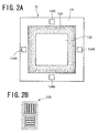
FIG. 2A is a top view of an example of the configuration
of a density filter;
FIG. 2B is a view of an example of marks formed on a
density filter;
FIG. 3A to FIG. 3I are views of variations of the
configuration of the light-attenuating part of a density
filter;
FIG. 4A and FIG. 4B are views of the configuration of
an illumination profile detection sensor;
FIG. 5 is a view for explaining a process of production
when producing a reticle (working reticle) using a master
reticle;
FIG. 6 is a view of the arrangement of optical members
from the blinds to the substrate in FIG. 1;
FIG. 7 is a view of changes in the width of the image
of a light-attenuating part of a density filter when changing
the illumination σ and other illumination conditions;
FIG. 8 is a view of an alignment mechanism of a reticle;
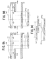
FIG. 9A to FIG. 9C are views for explaining a method
of adjustment of the profile of exposure;
FIG. 10A to FIG. 10C are views for explaining a method
of adjustment of the profile of exposure;
FIG. 11A to FIG. 11C are views for explaining a method
of adjustment of the profile of exposure;
FIG. 12A to FIG. 12C are views for explaining a method
of adjustment of the profile of exposure;
FIG. 13 is a view of another example of a configuration
for forming a slanted profile;
FIG. 14 is a view of the OPE characteristic when changing
the density of patterns with a pattern size of 360 nm and the
illumination σ;
FIG. 15 is a view of the OPE characteristic when changing
the density of patterns with a pattern size of 200 nm and the
illumination σ;
FIG. 16 is a view of the change in the profile of exposure
when changing the illumination σ; and
FIG. 17 is a view of an amount of exposure at overlay
parts when changing the illumination σ.
BEST MODE FOR WORKING THE INVENTION
Below, an explanation will be given of an embodiment
of the present invention with reference to the drawings. FIG.
1 is a view of the general configuration of an exposure apparatus
according to an embodiment of the present invention. The
exposure apparatus is a step-and-repeat type stitch projection
exposure apparatus. Further, in the following explanation,
the XYZ orthogonal coordinate system shown in FIG. 1 is set
and the positional relationships of the members explained while
referring to the XYZ orthogonal coordinate system. The XYZ
orthogonal coordinate system is set so that the X-axis and
the Z-axis become parallel to the paper surface and so that
the Y-axis becomes the direction perpendicular to the paper
surface. Further, the XYZ coordinate system in the figure is
set so that the XY plane becomes a plane parallel to the
horizontal surface and the Z-axis becomes the vertical
direction.
In FIG. 1, the ultraviolet pulse light IL of the light
from a light source 100 (here, a KrF excimer laser with a
wavelength of 248 nm) (hereinafter referred to as the "exposure
light IL") passes through a beam matching unit (BMU) 101
including movable mirrors etc. for matching of the position
of the optical path with the illumination optical system 1
and enters a variable light-attenuator 103 serving as a
light-attenuator through a pipe 102.
A main control system 9 controls the exposure of the
resist on the substrate 4 by communicating with the light source
100 to start and stop emission of light and control the output
as determined by the oscillation wavelength and the pulse
energy and to adjust the light-attenuation rate of the variable
light-attenuator 103 with respect to the exposure light IL
in stages or continuously.
The exposure light IL passing through the variable
light-attenuator 103 passes through a beam shaping optical
system comprised of lens systems 104 and 105 arranged along
a predetermined optical axis and enters an optical integrator
(homogenizer) 106. In this example, a fly-eye lens is used
as the optical integrator 106, so below the optical integrator
will also be called a "fly-eye lens 106". Here, the instead
of using a fly-eye lens as the optical integrator 106, it is
also possible to employ a rod integrator (inside surface
reflection type integrator) or a diffraction optical element
etc. Further, two fly-eye lenses 106 may be arranged in series
to enhance the uniformity of illumination profile.
An aperture stop system 107 is arranged at the emission
surface of the fly-eye lens 106. The aperture stop system 107
includes a circular aperture stop for normal illumination,
an aperture stop for modified illumination comprised of a
plurality of small offset apertures, an aperture stop for
annular illumination, etc. arranged in a switchable manner.
Therefore, in this example, the profile of exposure of the
exposure light IL on the pupil plane of the illumination optical
system (magnitude (corresponding to illumination σ) or shape
of the secondary light source), that is, the illumination
conditions of a master reticle Ri, can be freely changed by
the aperture stop system 107. Further, instead of the aperture
stop system 107 or in combination with it, it is possible to
arrange between the light source 100 (in particular the
variable light attenuator 103 or the lens systems 104 and 105)
and optical integrator 106, to give a profile of exposure light
IL at different areas on the pupil plane of the illumination
optical system 1, a plurality of diffraction optical elements
arranged switchably in the illumination optical system or a
plurality of prisms (conical prisms, polyhedron prisms, etc.)
at least one of which is movable along the optical axis AX
of the illumination optical system 1 and an optical unit
(illumination condition changing device) including at least
one zoom optical system so as tomake the distance in the optical
axis direction of the illumination optical system 1 variable
so as to make the profile of intensity of the exposure light
IL on the incident surface variable when the optical integrator
106 is a fly-eye lens and make the incident angle range of
the exposure light IL on the incident surface variable when
the optical integrator 106 is an inside surface reflection
type integrator and thereby suppress the loss in the amount
of light accompanying a change of the illumination conditions.
Further, in this example, the plurality of light source images
(imaginary images) formed by the inside surface reflection
type integrator are also called "secondary light sources".
Further, the changes in the illumination conditions in this
example are not limited to the illumination σ, that is, the
magnitude of the secondary light sources, and includes changes
in its shape as well.
The illumination light IL emitted from the fly-eye lens
106 and passing through a predetermined aperture stop of the
aperture stop system 107 enters a beam splitter 108 having
a high transmittance and a low reflectance. The light reflected
at the beam splitter 108 enters an integrator sensor 109
comprised of a photoelectric detector. The detection signal
of the integrator sensor 109 is supplied through a not
illustrated signal line to the main control system 9.
The transmittance and reflectance of the beam splitter
108 are measured to a high accuracy in advance and stored in
a memory in the main control system 9. The main control system
9 is designed to be able to monitor the intensity (or amount)
on the substrate 4 of the exposure light IL indirectly passing
through theprojection optical system 3 by the detection signal
of the integrator sensor 109.
The exposure light IL passing through the beam splitter
108 enters a reticle blind mechanism 110. The reticle blind
mechanism 110 is comprised of four movable blinds 111
(light-blocking plates) 111 (A-D) and their drive mechanisms
(for example, linear motors etc.) In this embodiment, the
reticle blind mechanism 110 has the four blinds 111 arranged
at a plane substantially conjugate with the pattern formation
surface of a master reticle Ri. By setting these four blinds
111 at suitable positions, a rectangular illumination area
is formed in the field of the projection optical system 3 (in
this case, circular). Further, in the illumination optical
system 1, the four blinds 111 may also be arranged separated
from the plane conjugate with the pattern formation surface
of the master reticle Ri, for example, substantially conjugate
with a density filter Fi.
The exposure light IL shaped into a rectangle by the
blinds 111 of the reticle blind mechanism 110 enters the density
filter Fj serving as the setting device (light-attenuating
member) carried on the filter stage FS. In this embodiment,
the density filter Fj is arranged away from the plane
substantially conjugate with the pattern formation surface
of the master reticle Ri in the reticle blind mechanism 110,
that is, in the illumination optical system 1, by exactly a
predetermined distance. The density filters Fj (here comprised
of F1 to F9) is configured basically as shown in FIG. 2A. FIG.
2A is a top view of an example of the configuration of a density
filter Fj. This density filter Fj is comprised of a
light-transmitting substrate such as quartz glass,
fluorine-doped quartz glass, etc. on which is formed a
light-blocking part 121 on which chrome or another
light-blocking material is deposited, a light-transmitting
part 122 on which no light-blocking material is deposited,
and a light-attenuating part (attenuating part) 123 on which
the light-blocking material is deposited while changing the
probability of presence.
The light-attenuating part 123 has the light-blocking
material deposited on it in dots. The size of the dots becomes
less than the resolution limit of the optical system having
the plurality of optical elements (112 to 116) arrangedbetween
the density filter Fj and the master reticle Ri in this example
in the state where the density filter Fj is placed at theposition
shown in FIG. 1. The dots are formed to increase in probability
of presence so that the light-attenuation rate becomes higher
linearly at a slant from the inside (light-transmitting part
122 side) to the outside (light-blocking part 121 side).
However, these dots may also be formed to increase in
probability of presence so that the light-attenuating rate
becomes higher in a curve from the inside to the outside.
The method of arrangement of the dots is preferably not
by arrangement of dots by the same pitch P at predetermined
areas giving the same transmittance, but by arrangement by
addition to P of a random number R having a Gaussian profile
generated for each dot, that is, a P+R system. The reason is
that diffracted light is produced by the arrangement of dots.
In some cases, the numerical aperture (NA) of the illumination
system is exceeded and light does not reach the photosensitive
substrate and therefore theerror from the design transmittance
becomes large.
Further, the sizes of the dots are preferably all the
same. The reason is that if several sizes of dots are used,
when error occurs from the design transmittance due to the
afore-mentioned diffraction, the error becomes complicated,
that is, correction of the transmittance becomes complicated.
Note that a density filter is preferably produced by a high
speed electron beam lithography system so as to reduce the
error in the dot shape. Further, the shape of the dots is
preferably a rectangular shape (square shape) for which proces s
errors in shape can be easily measured. This has the advantage
of easy correction of the transmittance in the case of any
measurable shape error.
The light-blocking part 121 is formed with a plurality
of alignment marks 124A, 124B, 124C, and 124D. These marks
124A, 124B, 124C, and 124D, as shown in FIG. 2A, can be formed
by removing parts of the light-blocking part 121 of the density
filter Fj to form rectangular or other shaped apertures
(light-transmitting parts) 124A, 124B, 124C, and 124D. Further,
it is also possible to use a mark shown in FIG. 2B. FIG. 2B
is a top view of an example of a mark formed on a density filter
Fj. In FIG. 2B, a slit mark 125 comprised of a plurality of
slit-shaped apertures is employed. This slit mark 125 is
comprised of a combination of a mark element comprised of slits
formed in a Y-direction aligned in an X-direction and a mark
element comprised of slits formed in an X-direction aligned
in a Y-direction for measurement of the positions in the
X-direction and Y-direction. The positions and the projection
magnification of the density filter Fj are adjusted based on
the results of measurement of the positional information of
the marks 124A, 124B, 124C, and 124D.
Further, the number of marks set at the density filter
is not limited to four. It is sufficient to set one or more
in accordance with the accuracy of setting etc. of the density
filter. Further, in this example, the density filter was
arranged so as to substantially match with the optical axis
of the illumination optical system at its center and four marks
were provided symmetrically with respect to the center (optical
axis), but when providing a density filter with a plurality
of marks, it is preferable to arrange the marks not to become
point symmetric about the center or to arrange a plurality
of marks point symmetrically and form a separate recognition
pattern. This is because, when arranging a density filter in
an illumination optical system, measuring the energy profile,
then taking out the density filter, correcting it, and
resetting i t, since the density filter is corrected considering
the optical characteristics of the illumination optical system
(distortion etc.), the correction would become meaningless
if the density filter were reset rotated in position. This
arrangement enables the density filter to be reset at the
original state.
The filter stage FS indexes or moves the held density
filter Fj in the XY plane in the rotational direction and the
translational direction. The X-coordinate, Y-coordinate, and
rotational angle of the filter stage FS are measured by not
shown laser interferometers. The operation of the filter stage
FS is controlled by the measured values and the control
information from the main control system 9. Further, in the
present embodiment, the filter stage FS is configured to be
movable in the Z-direction.
As explained above, the light-attenuating part 123 of
a density filter Fj has the light-blocking material deposited
on it in dots. To prevent the dots from being resolved on the
reticle, the density filter Fj is arranged at a position
defocused by a predetermined amount from the plane conjugate
with the pattern formation surface of the master reticle.
Therefore, if using the aperture stop system 107 to change
the emission side numerical aperture (illumination σ) of the
illumination optical system 1 to change the incident angle
(incident angle range) of the light beam on the density filter
Fj, the width of the image of the light-attenuating part 123
on the master reticle Ri on the substrate 4 will change and
in turn the widths of the overlay parts on the substrate 4
will change. Therefore, in the present embodiment, the change
in the widths of the overlay parts is corrected by controlling
the amount of defocus of the density filter Fj with respect
to the plane conjugate with the pattern formation surface of
the master reticle. Note that the details of the method of
control of the amount of defocus will be explained later.
Further, even if changing not only the magnitude of the
illumination σ, that is, the secondary light source, but also
its shape, the incident angle range of the light beam on the
density filter Fj will similarly change.
For the position of the density filter Fj in the
Z-direction and the amount of tilt in the Z-direction, a device
for detecting by an imaging element the masks of the density
filter Fj provided at least in part at the sample holder 5
is used to measure the marks 124A, 124B, 124C, and 124D or
themark 125 at apluralityof Z-directions bymoving the density
filter Fj in the optical axis direction. The Z-position giving
the largest signal intensity or signal contrast is designated
as the best focus position, and the amount of defocus is
controlled based on that best focus position.
In the present embodiment, a shelf-like filter library
16a is arranged at the side of the filter stage FS. The filter
library 16a has L number (L is a natural number) of support
shelves 17a successively arranged in the Z-direction. Density
filters F1, ..., FL are carried on the support shelves 17a.
The filter library 16a is supported to be movable in the
Z-direction by a slider 18a. A loader 19a able to freely rotate
and provided with an arm able to move in a predetermined range
in the Z-direction is arranged between the filter stage FS
and the filter library 16a. The main control system 9 adjusts
the position of the filter library 16a in the Z-direction
through the slider 18a, then controls the operation of the
loader 19b to enable transfer of desired density filters F1
to FL between the desired support shelves 17a of the filter
library 16a and the filter stage FS. While details are explained
later, the master reticle Ri is any of a plurality of master
reticles R1 to RN and is a reticle formed with parent patterns
P1 to PN dividing the parent pattern 36.
In the present embodiment, as shown in FIG. 3A to FIG.
3I, a total of nine density filters Fj, that is, F1 to F9,
are provided. FIG. 3A to FIG. 3I are views of the configurations
of density filters provided at the exposure apparatus according
to the embodiment of the present invention. These differ from
each other in the shapes or positions of the light-attenuating
parts 123 and are selectively used in accordance with whether
there are portions where the images of patterns overlap between
adjoining shot areas at the four sides of the shot areas to
be exposed (stitched parts).
That is, in the case of a shot area array of a matrix
of p (rows) x q (columns), the density filter of FIG. 3A is
used for the shot area (1, 1), the density filter of FIG. 3B
is used for the shot (1, 2 to q-1), the density filter of FIG.
3C is used for the shot (1, q), the density filter of FIG.
3D is used for the shot (2 to p-1, 1), the density filter of
FIG. 3E is used for the shot (2 to p-1, 2 to q-1), the density
filter of FIG. 3F is used for the shot (2 to p-1, q), the density
filter of FIG. 3G is used for the shot (p, 1), the density
filter of FIG. 3H is used for the shot (p, 2 to q-1), and the
density filter 3I is used for the shot (p, q).
Further, the density filter Fj is not limited to the
above nine types. It is possible to employ ones having other
shapes of light-attenuating parts 123 in accordance with the
shot shapes or shot arrays.
If the density filter Fj is made able to be used rotated
90 degrees or 180 degrees, by preparing for example the three
types of the density filter Fj of FIG. 3A, FIG. 3B, and FIG.
3E, other density filters become unnecessary. Further, by using
the single density filter Fj shown in FIG. 3E (that is, the
one with the detailed configuration shown in FIG. 2A),
selectively setting the positions of the four blinds 111 of
the reticle blind mechanism 110, or using the light-blocking
stripes of the master reticle Ri and blocking one or more of
the four sides of the light-attenuating part 123 by the
corresponding blinds 111, it is possible to realize the
functions of the density filters shown in FIG. 3A to FIG. 3I
and other density filters by a single density filter.
Further, the density filter Fj is not limited to one
comprised of a glass substrate formed with a light-attenuating
part or light-blocking portion by chrome or another
light-blocking material. Use may also be made of one using
liquid crystal elements etc. to enable the positions of the
light-blocking part or light-attenuating part and the
light-attenuating characteristics of the light-attenuating
part to be changed in accordance with need. In this case, there
is no longer a need to prepare several density filters and
various demands in the specifications of the working reticles
(microdevices) produced can be flexibly dealt with.
The exposure light IL passing through a density filter
Fj travels via a reflection mirror 112 and condenser mirror
system 113, an imaging lens system 114, a reflection mirror
115, and a main condenser lens system 116 to strike an
illuminated area (area illuminated by exposure light IL on
master reticle Ri) similar to the rectangular aperture of the
blinds 111 on the circuit pattern area of the master reticle
Ri. That is, the plane where the aperture of the blinds 111
is arranged becomes substantially conjugate with the pattern
formation surface of the master reticle Ri due to the combined
system of the condenser mirror system 113, imaging lens system
114, and main condenser lens system 116.
Note that in the present embodiment, at least one of
the condenser mirror system 113, imaging lens system 114, and
main condenser lens system 116 is configured to be movable
so as to enable change of the optical characteristics (focus
position, aberration, etc.) of the illumination optical system
1, in particular the parts arranged between the density filter
Fj, and the master reticle Ri. The optical characteristics
are controlled (adjusted) under the control of the main control
system 9. The optical characteristics of at least part of the
illumination optical system 1, that is, the optical systems
112 to 116 (corresponding to the later explained optical
members) are made variable (adjustable) so as to correct a
change in the width of the image on the substrate 4 of the
light-attenuating part 123 of the density filter Fj on the
master reticle Ri occurring due to a change in the illumination
conditions of the master reticle Ri due to the illumination
system 1 (that is, the above-mentioned aperture stop system
107 or optical unit) and in turn a change in the widths of
the overlay parts on the substrate 4.
In this way, in the present embodiment, to correct a
change in the image of the light-attenuating part 123, the
filter stage FS is configured to be movable in the Z-direction
and the optical characteristics of the condenser lens system
113 etc. are configured to be variable. To correct a change
in the width of image of the light-attenuating part 123 of
the density filter Fj, it is also possible to just control
the position of the density filter Fj in the Z-direction or
just adjust the optical characteristics of the condenser lens
system 113 etc. Further, it is possible to combine control
of the position of the density filter Fj in the Z-direction
and adjustment of the optical characteristics of the condenser
lens system 113 etc.
The exposure light IL emitted from the illumination
optical system 1 illuminates a master reticle Ri held on the
reticle stage 2. The reticle stage 2 holds the i-th (i = 1
to N) master reticle Ri. A shelf-like reticle library 16b is
arranged at the side of the reticle stage 2. This reticle library
16b has N number (N is a natural number) of support shelves
17b successively arranged in the Z-direction. Master reticles
R1, ..., RN are carried on the support shelves 17b.
The reticle library 16b is supported to be movable in
the Z-direction by a slider 18b. A loader 19b able to freely
rotate and provided with an arm able to move in a predetermined
range in the Z-direction is arranged between the reticle stage
2 and the reticle library 16b. The main control system 9 adjusts
the position of the reticle library 16b in the Z-direction
through the slider 18b, then controls the operation of the
loader 19b to enable transfer of desired master reticles F1
to FL between the desired support shelves 17b of the reticle
library 16b and the reticle stage 2.
The image of the patterns in the illuminated area of
the master reticle Ri is projected on the surface of the
substrate for the working reticle (blank) 4 at a reduction
rate 1/α (α is for example 5, 4, etc.) through a projection
optical system 3.
The reticle stage 2 moves the held master reticle Ri
in the XY plane in the rotational direction and the
translational direction. The reticle stage 2 is provided with
not shown laser interferometers. These laser interferometers
are used to measure the X-coordinate, Y-coordinate, and
rotational angle of the reticle stage 2. The measured values
and control information from the main control system 9 are
used for control of the operation of the reticle stage 2. Further,
the reticle stage 2 is configured to be movable in the optical
axis AX direction of the projection optical system 3 and is
configured to enable change of the angle with respect to the
optical axis AX. Due to this, it is possible to adjust the
position and posture of the master reticle Ri in the Z-direction.
These operations are controlled by the control information
from the main control system 9.
On the other hand, the substrate 4 serving as the
sensitive object is prevented from positional deviation due
to deformation of the substrate by being placed on a holder
comprised of three pins without suction or with soft suction.
The substrate holder is affixed on the sample table 5. The
sample table 5 is affixed on the substrate stage 6. Note that
as the substrate holder, it is also possible to use a pin chuck
holder etc. to hold the substrate 4. The sample table 5 matches
the surface of the substrate 4 with the imaging plane of the
projection optical system 3 by control of the focal position
(position in optical axis AX direction) and angle of tilt of
the substrate 4 by an auto focus system. The sample table 5
has affixed to it an illumination profile detection sensor
(so-called illumination uniformity sensor) for detecting the
illumination profile of the exposure light IL on a positioning
use fiducial mark member 12 and substrate 4. Further, the
substrate stage 6 moves and positions the sample table 5
(substrate 4) in the X-direction and Y-direction on the base
7 by for example linear motors.
Above the sample table 5 are fixed movable mirrors 8m.
The movable mirrors 8m are provided with laser interferometers
8 facing them. Note that in FIG. 1, while the illustration
is simplified, the movable mirrors 8m include a movable mirror
extending in the X-direction and a movable mirror extending
in the Y-direction above the sample table 5 and each of these
movable mirrors is provided with a laser interferometer facing
it. The laser interferometers 8 are used to measure the
X-coordinate, Y-coordinate, and rotational angle of the sample
table 5. The measured values are supplied to a stage control
system 10 and main control system 9. The stage control system
10 controls the operation of the linear motors etc. of the
substrate stage 6 based on the measured values and the control
information from the main control system 9. Further, while
the illustration is omitted in FIG. 1, the measurement results
from the laser interferometer provided at the reticle stage
2 are supplied to the main control system 9. In accordance
with the measurement results, the main control system 9
controls the X-coordinate, Y-coordinate, rotational angle,
Z-coordinate, and angle with respect to the optical axis AX
of the reticle stage 2. Note that instead of the movablemirrors,
it is also possible to use reflecting surfaces formed by
polishing the end faces (side faces) of the sample table 5
to a mirror finish.
Next, the details of the illumination profile detection
sensor 126 will be explained. FIG. 4A and FIG. 4B are views
of the configuration of the illumination profile detection
sensor 126. The illumination profile detection sensor 126 is
for measuring the spatial profile of the exposure light IL,
that is, the profile of intensity (illumination profile) of
the exposure light, by making the substrate stage 6 move in
the plane horizontal to the substrate 4 in a state illuminated
by the exposure light IL through the projection optical system
3. As shown in FIG. 4A, the illumination profile detection
sensor 126 is comprised of a light-blocking plate 55 having
a rectangular (in the present embodiment, square) aperture
(or pinhole) 54 below which a photoelectric sensor 56 is
provided. The detection signal of the photoelectric sensor
56 is output to the main control system 9. Further, it is also
possible to not provide the photoelectric sensor 56 below the
aperture 54, but to guide light by a light guide etc. and detect
the amount of received light by a photoelectric sensor etc.
at another portion.
The light-blocking plate 55 is normally comprised of
a quartz or other substrate on which chrome (Cr) or other metal
is deposited, but if depositing chrome or another metal, the
reflectance of the exposure light on the light-blocking plate
55 is high and the amount of reflection of the exposure light
is great. As a result, flares occur due to the reflected light
of the light-blocking plate 55 being reflected by the
projection optical system or reticle. The illumination profile
detection sensor 126 is provided for measuring the illumination
profile of the exposure light when the substrate 4 is exposed.
It is most preferable to measure the illumination profile of
the exposure light at the time of actual exposure. However,
when measuring the illumination profile of exposure light,
if the situation differs from the situation at the time of
actual exposure, that is, if the situation is one in which
the amount of reflection of the exposure light becomes greater,
it is not possible to accurately measure the illumination
profile of the exposure light at the time of actual exposure.
Therefore, in the present embodiment, to make
measurement as close as possible to the actual illumination
profile of the exposure light at the time of exposure, the
reflectance on the top surface of the light-blocking plate
55 is made substantially the same extent as the reflectance
of the substrate 4 so as to reduce the effect due to the reflected
light. The top surface of the light-blocking plate 44 is formed
with a film having a reflectance of the same extent as the
reflectance of the substrate 4 in the wavelength band of the
exposure light. To realize this film, for example, as shown
in FIG. 4B, it is possible to deposit on the quartz transparent
substrate 57 chrome 58, form on the chrome 58 a thin film 59
of chrome oxide, and coat above this a photoresist 60 the same
as the photoresist coated on the substrate 4 to the same
thickness. The reflectance of the top surface of this
light-blocking plate 55 can be adjusted by suitably selecting
not only the material of the film formed on the surface, but
also the thickness and configuration (number of layers, layer
thicknesses, materials of layers, etc.) When the substrate
4 is formed with an antireflection film etc., the reflectance
of the top surface of the light-blocking plate 55 is set
considering all of the conditions as well.
By using such an illumination profile detection sensor
126 to measure the exposure light passing through the aperture
54 formed in the light-blocking plate 55 while making the
substrate stage 6 move in a plane horizontal to the surface
of the substrate 4, it is possible to measure an illumination
profile substantially the same as the illumination profile
of the exposure light at the time of actual exposure.
Further, the main control system 9 has connected to it
a storage device 11 such as a magnetic disk drive. The storage
device 11 stores an exposure data file. The exposure data file
records design information of the master reticles R1 to RN,
the positional relationship among the master reticles R1 to
RN, the correspondence of the density filters F1 to FL to the
master reticles R1 to RN, the alignment information, etc.
The exposure apparatus according to the present
invention uses a plurality of master reticles to expose a
plurality of shot areas with peripheral parts partially
overlapping on the substrate. That is, it performs stitch
exposure of shots. This exposure apparatus is used not only
when producing a semiconductor integrated circuit, but also
when producing a reticle. Further, it is also possible to
perform stitch exposure at a single shot area using a plurality
of patterns. Here, the explanation will be given of the method
of producing a reticle produced using this master reticles
Ri and this exposure apparatus, that is, the working reticle.
FIG. 5 is a view for explaining the process of production
when producing a reticle (working reticle) using master
reticles Ri. The working reticle 34 shown in FIG. 5 is the
finally produced reticle. The working reticle 34 is comprised
of a light-transmitting substrate made of quartz glass or the
like (blank) on one surface of which is formed a master pattern
27 for transfer by chrome (Cr), molybdenum silicide (MoSi2
etc.), or another mask material. Further, two alignment marks
24A and 24B are formed so as to straddle the master pattern
27.
The working reticle 34 is used in reduction projection
of 1/β (where β is an integer larger than 1 or a half integer
etc., for example, 4, 5, or 6) through a projection optical
system of an optical type projection exposure apparatus. That
is, in FIG. 5, a reduced image 27W of 1/β times the master
pattern 27 of the working reticle 34 is exposed on each shot
area 48 of a wafer W coated with a photoresist, then developed
or etched etc. to form a predetermined circuit pattern 35 on
each shot area 48.
In FIG. 5, first the circuit pattern 35 of a certain
layer of the semiconductor device to be finally produced is
designed. The circuit pattern 35 forms various line-and-space
patterns (or isolated patterns) in a rectangular area with
widths of perpendicular sides of dX and dY. In this embodiment,
the circuit pattern 35 is enlarged β times to prepare a master
pattern 27 comprised of a rectangular area with widths of
perpendicular sides of β·dX and β·dY in the image data of the
computer. The multiple β is a reciprocal of the reduction rate
(1/β) of the projection exposure apparatus where the working
reticle is to be used. Further, the image is inverted and
enlarged at the time of inversion projection.
Next, the master pattern 27 is enlarged α-fold (α is
an integer larger than 1 or a half integer, for example, 4,
5, or 6) to prepare, in the image data, a parent pattern 36
comprised of a rectangular area with widths of perpendicular
sides of α·β·dX and α·β·dY. The parent pattern 36 is then
partitioned longitudinally and laterally into α number of
sections to prepare α x α number of parent patterns P1, P2,
P3..., PN (N = α2) in the image data. In FIG. 5, the case where
α = 5 is shown. Note that the multiple α is the reciprocal
of the projection magnification of the projection exposure
apparatus used for production of the working reticle 34 (in
this example, the magnification of the projection optical
system 3 in FIG. 1). Further, the divisor α of the parent pattern
36 does not necessarily have to match the magnification α of
the master pattern 27 to the parent pattern 36. The number
of partitions in the vertical and horizontal directions do
not have to be made the same either. Next, these parent patterns
Pi (i = 1 to N) are used to produce lithographic data for an
electron beam lithography system (or laser beam lithography
system) and these parent patterns Pi are transferred on to
the master reticle Ri as parent masks at equal magnification
rates.
For example, when producing one master reticle R1, a
thin film of chrome or molybdenum silicide or other mask
material is formed on a light-transmitting substrate of quartz
glass etc., an electron beam resist is coated on this, then
the electron beam lithography system is used to draw an equal
magnification latent image of the first parent pattern P1 on
the electron beam resist. Next, the electron beam resist is
developed, then is etched and the resist peeled off etc. to
form the parent pattern P1 on the pattern area 20 on the master
reticle R1.
Further, the master reticle R1 is formed with alignment
marks 21A and 21B comprised of 2-dimensional marks in a
predetermined positional relationship with respect to the
parentpattern P1. In the sameway, an electronbeamlithography
system is used to form parent patterns Pi and alignment marks
21A and 21B on other master reticles Ri. These alignment marks
21A and 21B are used for positioning with respect to the
substrate or density filter.
The parent patterns Pi drawn by the electron beam
lithography system (or laser beam lithography system) in this
way are patterns of the master pattern 27 enlarged α-times,
so the amount of the lithographic data is reduced to about
1/α2 compared with when directly drawing the master pattern
27. Further, the minimum line width of the parent patterns
Pi is α-times (for example 5-times or 4-times) the minimum
line width of the master pattern 27, so the parent patterns
Pi can be drawn in a short time and at a high accuracy by an
electron beam lithography system using conventional electron
beam resists. Further, by producing N number of master reticles
R1 to RN at one time, it is possible to produce the number
of necessary working reticles 34 by repeatedly using them,
so the time for producing the master reticles R1 to RN does
not become a large burden.
The working reticle 34 is produced by using the thus
produced N number of master reticles Ri and transferring the
1/α-size reduced images of the parent patterns Pi of the master
reticles Ri while stitching them together.
When producing a working reticle 34 explained above,
for example to improve the OPE characteristic explained above,
the illumination σ and other illumination conditions are set
in accordance with the density of the patterns etc. formed
on the master reticles Ri. When changing the illumination σ
and other illumination conditions, a change in the width of
the light-attenuating part 123 of the density filter Fj at
the master reticles Ri and in turn a change in the widths of
the overlay parts on the substrate 4 occur as explained above.
Below, the method of correction of the change in the widths
will be explained in detail.
FIG. 6 is a view of the optical members arranged in the
optical path from the blinds 111 to the substrate 4 in FIG.
1, while FIG. 7 is a view of the change in the width of the
light-attenuating part 123 of a density filter Fj when changing
the illumination σ and other illumination conditions.
As shown in FIG. 6, the blinds 111 and the density filter
Fj are arranged near a plane PL1 conjugate with the master
reticle Ri (hereinafter referred to as the "reticle conjugate
plane PL1"). The projection magnification of the optical
members between this reticle conjugate plane PL1 and master
reticle Ri (condenser lens system 113, imaging lens system
114, and main condenser lens system 116) is designated as M
and the projection magnification of the projection optical
system 3 arranged between the master reticle Ri and the
substrate 4 is designated as N (=1/α). Note that in the following
explanation, it is assumed that the optical members (optical
system) are enlargement types, M=2, N=1/4, and the numerical
aperture of the projection optical system 3 is 0.75.
Further, as shown in FIG. 7, the width of the
light-attenuating part 123 is designated as [a] and the amount
of defocus of the density filter Fj from the reticle conjugate
plane PL1 is designated as [d]. Here, if designating the
incident angle of the exposure light IL as , the numerical
aperture NA1 of the exposure light IL at the reticle conjugate
plane PL1, the numerical aperture NA2 of the exposure light
IL at the position of the master reticle Ri, and the numerical
aperture NA3 of the exposure light IL at the position of the
substrate 4 are expressed by the following equation (1) to
equation (3):
NA1=sin
NA2=sin/M
NA3=sin/(M·N)
Further, since the density filter Fj is defocused with
respect to the reticle conjugate plane PL1, the width WG1 of
the light-attenuating part 123 at the reticle conjugate plane
PL1, the width WG2 of the light-attenuating part 123 at the
position of the master reticle Ri, and the width WG3 of the
image of the light-attenuating part 123 at the position of
the substrate 4 become the following equation (4) to equation
(6) :
WG1=a+2·d·tan+b
WG2=(a+2·d·tan+b)·M
WG3=(a+2·d·tan+b)·M·N
Note that in equation (4) to equation (6), [b] is the
amount of blurring occurring due to aberration etc. of the
illumination optical system 1.
Here, as shown in FIG. 14, when transferring patterns
of a pattern size of 360 nm on the
substrate 4, the OPE
characteristic was the best when setting the illumination σ
to 0.55, that is, when the numerical aperture NA of the exposure
light IL on the
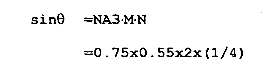
substrate 4 is 0.75x0.55=0.413. At this time,
the incident angle of the exposure light IL irradiating the
substrate 4 is found as follows from equation (3):
Further, to make the width WG of the light-attenuating
part 123 at the position of the substrate for example 1000
µm (1 mm), from equation (6), it is sufficient to set the width
[a] of the light-attenuating part 123, the amount of defocus
[d] of the density filter Fj from the reticle conjugate plane
PL1 and the amount of blurring [b] occurring due to the
aberration of the illumination optical system 1 etc. as follows
for example.
a=1368 µm
d=1500 µm
b=0 µm
Here, when transferring patterns with a pattern size
of 200 nm instead of patterns with a pattern size of 360 nm
on the
substrate 4, the OPE characteristic was the best when
setting the illumination σ at 0.85 as explained using FIG.
15, that is, when the numerical aperture NA3 of the exposure
light IL on the
substrate 4 is 0.75x0.85=0.638. At this time,
the incident angle of the exposure light IL irradiating the
substrate 4 is found as follows from equation (3):
In the past, when changing the illumination conditions
(in this example, the illumination σ, that is, the coherence
factor), the amount of defocus [d] of the density filter Fj
with respect to the reticle conjugate plane PL1 was not changed,
so if changing the illumination σ from 0.55 to 0.85, from
equation (6), the width WG3 of the image of the
light-attenuating part 123 at the position of the substrate
ended up increasing to 1189 µm.
Here, referring to equation (6), the width WG3 of the
image of the light-attenuating part 123 at the position of
the substrate 4 is determined by the width [a] of the
light-attenuating part 123, the amount of defocus [d] of the
density filter Fj from the reticle conjugate plane PL1, the
incident angle of the exposure light IL, the amount of blurring
[b] occurring due to aberration of the illumination optical
system 1, the enlargement magnification M of the optical
members between the reticle conjugate plane PL1 and the master
reticle Ri, and the reduction rate N of the projection optical
system 3. Therefore, by making at least one of these six
parameters variable, it becomes possible to adjust the width
WG3 of the image of the light-attenuating part 123 at the
position of the substrate 4. In the present embodiment, by
controlling the amount of defocus [d] of the density filter
Fj from the reticle conjugate plane PL1, which is easy to make
variable by the drive mechanism DR1 (see FIG. 6) among these
parameters, the width WG3 of the image of the light-attenuating
part 123 at the position of the substrate 4 is adjusted.
Specifically, if modifying equation (6), the following
equation (7) is obtained:
d=(WG3/(M·N)-a-b)/(2·tan)
In equation (7), if making WG3 1000 µm and making 18.6
degrees, [d] becomes 940 µm. Therefore, when changing the
illumination σ which had been set to 0.55 to transfer patterns
of a pattern size of 360 nm on a substrate 4 to 0.85, it is
sufficient to change the amount of defocus of the density filter
Fj with respect to the reticle conjugate plane PL1 from 1500
µm to 940 µm. In this way, in the present embodiment, by changing
the illumination conditions (for example, illumination σ) of
the master reticle Ri by the illumination optical system 1
so as to give the optimal OPE characteristic in accordance
with the size and density of patterns formed at a master reticle
Ri and adjusting the position of the density filter Fj in the
Z-direction, the patterns of a master reticle Ri are
transferred on the substrate 4 while adjusting the width WG3
of the image of the light-attenuating part 123 of the density
filter Fj on the substrate 4. Note that the main control system
9 preferably sets the optimal illumination conditions for each
pattern to be transferred on the substrate 4 by the aperture
stop system 107 or optical unit and adjusts the position of
the density filter Fj in the Z-direction based on the design
information of the master reticles R1 to RN stored in the
exposure data file in the storage device 11. Further, it is
also possible to find in advance the illumination conditions
of the illumination optical system 1 set for each of the master
reticles R1 to RN and the amount of defocus [d] of the density
filter Fj with respect to the reticle conjugate plane PL1 and
store the actually measured values (or calculated values) in
the storage device 11 linked with the master reticles R1 to
RN.
Further, when exposing reduced images of the master
reticles R1 to RN on the substrate 4 by projection in this
way, it is necessary to stitch the adjoining reduced images
with a high accuracy. For this alignment, the projection
exposure apparatus of the present embodiment is provided with
a reticle and substrate alignment mechanism.
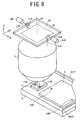
FIG. 8 shows the reticle alignment mechanism. In FIG.
8, a light-transmitting fiducial mark member 12 is affixed
near the substrate 4 on the sample table 5. Two cross-shaped
fiducial marks 13A and 13B are for example formed at a
predetermined interval in the X-direction on the fiducial mark
member 12. At the bottoms of the fiducial marks 13A and 13B
is placed an illumination system for illuminating the fiducial
marks 13A and 13B at the projection optical system 3 side by
illumination light branched from the exposure light IL. When
aligning a master reticle Ri, the substrate stage 6 of FIG.
1 is driven to position the fiducial marks 13A and 13B so that
the center point between the fiducial marks 13A and 13B on
the fiducial mark member 12 substantially registers with the
optical axis AX of the projection optical system 3 as shown
in FIG. 8.
Further, for example, two cross-shaped alignment marks
21A and 21B are formed so as to straddle the pattern area 20
of the pattern surface (bottom surface) of the master reticle
Ri in the X-direction. The distance between the fiducial marks
13A and 13B is set to be substantially equal to the distance
between images of the alignment marks 21A and 21B reduced by
the projection optical system 3. By illumination by
illumination light of the same wavelength as the exposure light
IL from the bottom of the fiducial mark member 12 in the state
with the center point between the fiducial marks 13A and 13B
substantially in register with the optical axis AX in the above
way, images of the fiducial marks 13A and 13B enlarged by the
projection optical system 3 are formednear the alignmentmarks
21A and 21B of the master reticle Ri.
Mirrors 22A and 22B are arranged above the alignment
marks 21A and 21B to reflect the illumination light from the
projection optical system 3 side in the ±X directions. Image
processing type alignment sensors 14A and 14B are provided
by a TTR (through-the-reticle) system so as to receive the
illumination light reflected by the mirrors 22A and 22B. The
alignment sensors 14A and 14B are each provided with an imaging
system and a 2-dimensional image pickup element such as a CCD
camera. The image pickup elements pick up the images of the
alignment marks 21A and 21B and the corresponding fiducial
marks 13A and 13B and supply image signals to an alignment
signal processing system 15 of FIG. 1.
The alignment signal processing system 15 processes the
image signals to find the amounts of positional deviation of
the alignment marks 21A and 21B in the X-direction and
Y-direction with respect to the fiducial marks 13A and 13B
and supplies the two positional deviations to the main control
system 9. The main control system 9 positions the reticle stage
2 so that the two positional deviations become symmetrical
and within predetermined ranges. Due to this, the alignment
marks 21A and 21B and in turn the master reticle Ri are
positioned with respect to the fiducial marks 13A and 13B.
In other words, the center (exposure center) of the
reduced image of the master reticle Ri obtained by the
projection optical system 3 is substantially positioned at
the center point between the fiducial marks 13A and 13B
(substantially the optical axis AX). In this state, the main
control system 9 of FIG. 1 stores the X-direction and
Y-direction coordinates (XF0, YF0) of the sample table 5
measured by the laser interferometers 8, whereby the alignment
operation of the master reticle Ri ends. After this, it is
possible to move any point on the sample table 5 to the exposure
center of the parent pattern Pi.
Further, as shown in FIG. 1, an image processing type
alignment sensor 23 is provided by an off-axis system at the
side of the projection optical system 3 to detect the position
of amark on the substrate 4. The alignment sensor 23 illuminates
a detection mark by illumination light of a wide band to which
the photoresist is not sensitive, picks up the image of the
detection mark by a two-dimensional image pickup element such
as a CCD camera, and supplies an image signal to the alignment
signal processing system 15. Further, the distance (base line
amount) between the detection center of the alignment center
23 and the center of the projected image of the pattern of
the master reticle Ri (exposure center) is found in advance
using a predetermined fiducial mark on the fiducial mark member
12 and stored in the main control system 9.
As shown in FIG. 8, two cross-shaped alignment marks
24A and 24B are formed at the ends of the substrate 4 in the
X-direction. After a master reticle Ri is aligned, the
substrate stage 6 is driven to successively move the fiducial
marks 13A and 13B and the alignment marks 24A and 24B on the
substrate 4 to the detection area of the alignment sensor 23
of FIG. 1 and measure the positional deviations of the fiducial
marks 13A and 13B and the alignment marks 24A and 24B with
respect to the detection center of the alignment sensor 23.
The results of the measurements are supplied to themain control
system 9. Using these measurement results, the main control
system 9 finds the coordinates (XP0, YP0) of the sample table
5 when the center point between the fiducial marks 13A and
13B is in register with the detection center of the alignment
sensor 23 and the coordinates (XP1, YP1) of the sample table
5 when the center point between the alignment marks 24A and
24B is in register with the detection sensor of the alignment
sensor 23. This ends the alignment operation of the substrate
4.
As a result, the distances between the center point
between the fiducial marks 13A and 13B and the center point
between the alignment marks 24A and 24B in the X-direction
and the Y-direction become (XP0-XP1, YP0-YP1). Therefore, by
driving the substrate stage 6 of FIG. 1 by exactly the distances
(XP0-XP1, YP0-YP1) with respect to the coordinates (XF0,YF0)
of the sample table 5 at the time of alignment of the master
reticle Ri, it is possible to bring the center point between
the alignment marks 24A and 24B of the substrate 4 (center
of substrate 4) into register with the center point between
the projected images of the alignment marks 21A and 21B of
the master reticle Ri (exposure center) with a high accuracy.
From this state, the substrate stage 6 of FIG. 1 may be driven
to move the sample table 5 in the X-direction and theY-direction
so as to expose a reduced image PIi of a parent pattern Pi
of the master reticle Ri at a desired position with respect
to the center of the substrate 4.
Further, when exposing one substrate 4, regardless of
the change of the master reticle Ri, the substrate 4 is placed,
without suction or with soft suction, on the sample table 5
comprised of the three pins, and the substrate stage 6 is made
to move by a super-low acceleration and a super-low speed so
that the position of the substrate 4 does not shift at the
time of exposure. Therefore, since the positional relationship
between the fiducial marks 13A and 13B and the substrate 4
does not change during the exposure of one substrate 4, when
switching the master reticle Ri, it is sufficient to position
the master reticle Ri with respect to the fiducial marks 13A
and 13B. There is no need to detect thepositions of the alignment
marks 24A and 24B on the substrate 4 for each master reticle.
Above, an explanation was given of the positioning of
a master reticle Ri and the substrate 4, but the master reticle
Ri and the density filter may also be positioned relative to
each other based on the resul ts of measurement of the positional
information of the marks 124A, 124B, 124C, and 124D and the
slitmark 125. At this time, a slight rotation sometimes occurs
in the substrate 4 due to the characteristics of the substrate
stage 6, the yawing error, and other error. Therefore, a slight
deviation occurs in the relative postures of the master reticle
Ri and the substrate 4. This error is measured in advance or
measured during actual processing and the reticle stage 2 or
substrate stage 6 controlled so that the postures of the master
reticle Ri and the substrate 4 are corrected to become in
register so as to cancel this error out.
By successively exposing reduced images of parent
patterns P1 to PN of the N number of master reticles R1 to
RN of FIG. 1 on the corresponding shot areas S1 to SN of the
substrate 4 in this way, the reduced images of the parent
patterns P1 to PN are exposed while being stitched with the
reduced images of the adjoining parent patterns. Due to this,
theprojected image 26 of the parent pattern 36 of FIG. 1 reduced
to 1/α is exposed and transferred on to substrate 4 at the
exposure area comprised of the plurality of shot areas with
peripheral parts partially overlapped. Next, the photoresist
on the substrate 4 is developed and etched and the remaining
resist pattern is peeled off, whereby the projected image 26
on the substrate 4 forms the master pattern 27 as shown in
FIG. 6 and the working reticle 34 is completed.
In the embodiment explained above, the illumination
conditions of the illumination optical system 1 were changed
in accordance with the pattern size and density of the patterns
formed on a master reticle Ri and the position of the density
filter Fj in the Z-direction (amount of defocus of the density
filter Fj with respect to the reticle conjugate plane) was
adjusted in accordance with the change in the illumination
conditions to adjust the width of the image of the
light-attenuating part 123 of the density filter Fj on the
substrate 4, that is, the widths of the overlay parts, and
successively transfer patterns of master reticles Ri on the
substrate 4 by a step-and-repeat operation so as to produce
a working reticle 34.
Here, if adjusting the defocus of the density filter
Fj, sometimes deviation occurs between the combined amount
of exposure at the overlay parts and the amount of exposure
at other than the overlay parts. In this case, by controlling
the relative positions of the blinds 111, density filter Fj,
master reticle Ri, and substrate 4, it is possible to adjust
the combined amount of exposure of the overlay parts. Below,
an example of the method of adjustment will be explained.
FIG. 9A to FIG. 9C, FIG. 10A to FIG. 10C, FIG. 11A to
FIG. 11C, and FIGS. 12A to 14C are views for explaining the
method of adjustment of the profile of the amount of exposure.
Note that in these figures, to facilitate understanding, only
theblinds, densityfilter, andmasterreticleareillustrated.
First, FIG. 9A to FIG. 9C will be explained.
FIG. 9A is a view of the relative positions of the density
filter and the master reticle when exposing a first shot area,
FIG. 9B is a view of the relative positions of the density
filter and the master reticle when exposing a second shot area
adjoining the first shot area, and FIG. 9C is a view of the
profile of amount of exposure in areas exposed when exposed
in the state shown in FIG. 9A and FIG. 9B.
In FIG. 9A to FIG. 9C, members the same as the members
shown in FIG. 1 are assigned the same notations. That is, in
FIG. 9A and FIG. 9B, F1 and F2 are density filters, 111A and
111B are blinds, and R1 and R2 are master reticles. Note that
in FIG. 9A and FIG. 9B, the density filters F1 and F2, the
blinds 111A and 111B, and the master reticles R1 and R2 are
shown centered about the optical axis AX of the projection
optical system 3. For facilitating understanding, the optical
axis AX is shown straight without bending. Further, in FIG.
1, the blinds 111A and 111B, the density filter Fj, and the
reticle Ri are arranged in that order along the optical axis
AX, but in FIG. 9A and FIG. 9B, to facilitate understanding,
the density filters F1 and F2 and the blinds 111A and 111B
are shown switched in order of arrangement. Further, for the
master reticles R1 and R2, to specify the positions of the
patterns formed on the master reticles R1 and R2, numerals
according to the positions shown in FIG. 9A to FIG. 9C are
assigned. Note that when specifying the pattern positions,
they are described below such as the pattern "1", pattern "2",
etc.
First, the case of exposure of the first shot area will
be explained with reference to FIG. 9A. In FIG. 9A, the exposure
light IL incident upon the density filter F1 has a uniform
profile of exposure in the plane vertical to the optical axis
AX, butif incident on the density filter F1, lightis attenuated
at the light-attenuating part 123, so after passing through
the density filter F1, the profile of exposure becomes that
with the notation PF1. Note that when showing the profile of
exposure at FIG. 9A to FIG. 9C, the axis showing the amount
exposure is made a direction parallel to the optical axis AX.
The exposure light passing through the density filter
F1 strikes the blinds 111A and 111B, whereby it is formed into
a predetermined shape. In the example shown in FIG. 9A, it
is formed into a shape illuminating the pattern "1" to the
pattern "11" formed on the master reticle R1. When the exposure
light passing through the blinds 111A and 111B strikes the
master reticle R1, an image reflecting the shapes of the
patterns is emitted as shown by notation Im1. Note that the
profile of exposure of the image Im1 becomes one given the
notation PF11. That is, the exposure light passing through
the light-transmitting part 122 has a constant profile of
exposure, but the exposure light passing through the
light-attenuating part 123 becomes a profile of exposure
linearly attenuating from the pattern "7" to the pattern "11".
Further, FIG. 9B shows the case of exposure of the second
shot area. As shown in FIG. 9B, after passing through thedensity
filter F2, the profile of exposure becomes the one assigned
the notation PF2. Note that in FIG. 9A and FIG. 9B, to facilitate
understanding, the profile of exposure PF1 and the profile
of exposure FP2 are shown as the same profiles.
The positions of the blinds 111A and 111B in the case
of exposure of the second shot area different from the positions
of the blinds 111A and 111B in the case of exposure of the
first shot area. That is, the blinds 111A and 111B form the
exposure light into a shape illuminating the pattern "7" to
the pattern "17" of the master reticle R2.
When the exposure light passing through the blinds 111A
and 111B strikes the master reticle R2, as shown by notation
Im2, an image reflecting the shapes of the patterns is emitted.
Note that the profile of exposure of the image Im2 becomes
that assigned the notation PF12. That is, the exposure light
passing through the light-transmitting part 122 is a constant
profile of exposure, but the exposure light passing through
the light-attenuating part 123 becomes a profile of exposure
linearly attenuating from the pattern "1" to the pattern "7".
The image Im1 shown in FIG. 9A and the image Im2 shown
in FIG. 9B are stitched in the positional relationship shown
in FIG. 9C. That is, the images of the pattern "7" to the pattern
"11" are overlapped and transferred by exposure to the overlay
part. If exposed in this way, ideally as shown by the notation
PF13 in FIG. 9C, the amount of exposure of the overlay part
becomes equal to the amount of exposure of the parts other
than the overlay part. Note that in FIG. 9C, the distance between
the exposure position of the first shot area and the exposure
position of the second shot area is called the "step pitch
SP1". That is, the step pitch SP1 is the distance for moving
the second shot area to the exposure position after exposure
of the first shot area. In the examples shown in FIG. 9A to
FIG. 9C, FIG. 10A to FIG. 10C, FIG. 11A to FIG. 11C, and FIG.
12A to FIG. 12C, the step pitch SP1 is set to 21 mm, that is,
21000 µm.
Note that in this embodiment, the "overlay part" means
a part where the peripheral parts of the shot areas overlap
on the substrate 4, a part where the images of the
light-attenuating parts 123 of the density filters Fj overlap
on the substrate 4, or a part where the images of the patterns
of the master reticles overlap on the substrate 4. In the above
explanation, these matched, so were not particularly
differentiated. However, in the following explanation, these
sometimes do not match, so when referring to simply an "overlay
part", this shall be deemed to mean mainly a part where the
peripheral parts of shot areas overlap on the substrate 4.
To differentiate from this, a part where the images of the
light-attenuating parts 123 of the density filters Fj overlap
on the substrate 4 will be sometimes referred to as a "reduced
light image overlap part" and a part where the images of the
patterns of the master reticles overlap on the substrate 4
will be referred to as a "pattern image overlap part".
Next, the method of adjustment of the exposure profile
will be explained with reference to FIG. 10A to FIG. 10C, FIG.
11A to FIG. 11C, and FIG. 12A to FIG. 12C. The method explained
below is a method of adjusting the amount of exposure at an
overlay part where peripheral parts of shots overlap by
changing the profile of the energy beam defined by the density
filter and the relative position with the patterns to be
transferred. More specifically, it adjusts the amount of
exposure at the overlay part by changing the relative positions
of the density filters and master reticles to change the width
of the reduced light image overlay part. In the following
description, the explanation will be given taking as an example
the case where the width of the overlay part and the reduced
light image overlay part is 1 mm, that is, 1000 µm.
In this case, the point that if the width of the reduced
image overlay part changes by 10 µm, the amount of exposure
changes by a rate of 1% should be noted. That is, 100%/1000
µm = 1%/10 µm. Note that in the explanation using FIG. 10A
to FIG. 10C, FIG. 11A to FIG. 11C, and FIG. 12A to FIG. 12C,
the master reticles R1 and R2 are made to move, but in this
case the point that the substrate 4 also moves along with
movement of the master reticles R1 and R2 should be noted.
In this case, the amount of movement of the substrate 4 is
1/α times the amount of movement of the master reticles R1
and R1 (where α is the reduction rate of the projection optical
system 3).
FIG. 10A to FIG. 10C are views of an example of the relative
positional relationship among the density filters, blinds,
and master reticles in the case of decreasing the width of
the reduced exposure overlay part so as to decrease the amount
of exposure of the overlay part. Note that in the following
explanation, for convenience, the explanation will be made
of the case of changing the positions of the blinds 111A and
111B and the master reticles R1 and R2 without changing the
positions of thedensity filters F1 andF2 to change the relative
positions of the density filters F1 and F2 and the master
reticles R1 and R2, but it is also possible to change the
positions of the density filters F1 and F2 to change the relative
positions without making the master reticles R1 and R2 move.
If now desiring to decrease the amount of exposure at
the overlay part by exactly 1%, it is sufficient to decrease
the width of the overlay part by exactly 10 µm. Therefore,
at the time of the exposure of the second shot area on the
substrate 4, the substrate 4 is made to move in a step from
the exposure position of the first shot area by exactly 21000
µm+10 µm = 21010 µm.
Further, as will be understood from a comparison of FIG.
9A and FIG. 10A, the blind 111A and the master reticle R1 are
moved in the D1 direction in FIG. 10A by exactly the amount
of one pattern formed on the master reticle R1. Therefore,
the pattern "1" of the master reticle R1 moves to the position
of the pattern "2" of the master reticle R1 shown in FIG. 9A.
Since the case of reducing the width of the overlay part by
exactly 10 µm is being considered here, the amount of movement
of the master reticle R1 should be made 5 µm converted to the
amount on the substrate 4. That is, since the reduction rate
of the projection optical system 3 is 1/α, it is sufficient
to make the master reticle R1 move by exactly 5 x α µm in a
certain direction, that is, the D1 direction in FIG. 10A. In
FIG. 10A, since only the blind 111A moves, the illuminated
area for the master reticle R1 also becomes narrower compared
with the case of FIG. 9A. As shown in FIG. 10A, in this case,
the image Im3 of the pattern "1" to the pattern "10" is formed.
After exposure of the first shot area, as explained above,
the substrate 4 is made to move by exactly 21010 µm to position
the second shot area at the exposure position. Further, the
blind 111B and the master reticle R2 are made to move from
the position shown in FIG. 9B in the direction with the overlay
part, that is, in the D2 direction in FIG. 10B, by exactly
5·α µm. As shown in FIG. 10B, in this case, the image Im4 of
only the pattern "8" to the pattern "17" is formed.
The image Im3 shown in FIG. 10A and the image Im4 shown
in FIG. 10B are stitched in the positional relationship shown
in FIG. 10C. That is, the image from the pattern "8" to the
pattern "10" is exposed at the overlay part. That is, by making
the step pitch SP1 of the substrate 4 SP1+SP2=21000 µm+10 µm
= 21010 µm and performing exposure by making the master reticles
R1 and R2 move in the D1 direction and D2 direction compared
with the case shown in FIG. 9A to FIG. 9C, the amount of exposure
at the overlay part is decreased. As shown in FIG. 10C, the
profile of the amount of exposure at the overlay part becomes
the profile PF23.
FIG. 11A to FIG. 11C are views of an example of the relative
positional relationship among the density filters, blinds,
and master reticles in the case of increasing the width of
the light image overlay part so as to increase the amount of
exposure of the overlay part. Note that in the same way as
the case of FIG. 10A to FIG. 10C, it is also possible to change
the positions of the density filters F1 and F2 to change the
relative positions without making the master reticles R1 and
R2 move.
If now desiring to increase the amount of exposure at
the overlay part by exactly 1%, it is sufficient to increase
the width of the overlay part by exactly 10 µm. Therefore,
at the time of the exposure of the second shot area on the
substrate 4, the substrate 4 is made to move in a step from
the exposure position of the first shot area by exactly 21000
µm-10 µm = 20990 µm.
Further, as shown in FIG. 11A, the blind 111A and blind
111B and the master reticle R1 are moved in the D3 direction
in the figure by exactly the amount of one pattern formed on
the master reticle R1, that is, 5·α µm. In FIG. 11A, the blind
111A and the blind 111B move, so the illuminated area for the
master reticle R1 becomes the same as the case of FIG. 9A.
As shown in FIG. 11A, in this case, the image Im5 of the pattern
"1" to the pattern "11" is formed.
After exposure of the first shot area, as explained above,
the substrate 4 is made to move by exactly 20990 µm to position
the second shot area at the exposure position. Further, the
blinds 111A and 111B and the master reticle R2 are made to
move from the position shown in FIG. 9B in the direction with
no overlay part, that is, in the D4 direction in FIG. 11B,
by exactly 5·α µm. As shown in FIG. 11B, in this case, the
image Im6 of the pattern "7" to the pattern "17" is formed.
These image Im5 and image Im6 are images similar to the
image Iml and image Im2 shown in FIG. 9A to FIG. 9C, but the
exposure profiles and the positions where the images are formed
on the substrate 4 differ. For example, comparing the image
Im5 in FIG. 11A and the image Im1 in FIG. 9A, the image Im1
has a constant exposure profile from the image of the pattern
"1" to the image of the pattern "6", but the image Im5 has
a constant exposure profile from the image of the pattern "1"
to the image of the pattern "7". That is, the location of the
constant exposure profile is one pattern's distance longer
compared with the case of the image Im1.
Further, the image Im1 is an exposure profile linearly
attenuating from the image of the pattern "7" to the image
of the pattern "11". The amount of exposure gently becomes
0 at the end of the image of the pattern "11". As opposed to
this, the image Im5 linearly attenuates from the image of the
pattern "8" to the image of the pattern "11". The section having
this profile is 1 pattern's distance shorter than the image
Im1. Further, itdiffers in the point that the amount of exposure
sharply becomes 0 from a certain value at the end of the image
of the pattern "11".
The image Im5 shown in FIG. 11A and the image Im6 shown
in FIG. 11B are stitched in the positional relationship shown
in FIG. 11C. That is, the image from the pattern "7" to the
pattern "11" is exposed at the overlay part. That is, by making
the step pitch SP1 of the substrate 4 SP1-SP3=21000 µm-10 µm
= 20990 µm and performing exposure by making themaster reticles
R1 and R2 move in the D3 direction and D4 direction compared
with the case shown in FIG. 9A to FIG. 9C, the amount of exposure
at the overlay part is increased.
In FIG. 11C, since the amount of exposure at the overlay
part of the profile PF31 of the image Im5 and the profile PF32
of the image Im6 increases, the profile of exposure at the
overlay part becomes the profile PF33.
Note that as shown in FIG. 11A and FIG. 11B, the blinds
111A and 111B are used to block part of the light-attenuating
parts 123 of the density filters F1 and F2, but this is because
there are no patterns at the corresponding parts of the mask.
As a result, in FIG. 11C, the width of the reduced light image
overlay part appears not to change, but when there are no blinds
111A and 111B or other light-blocking members, the width of
the reduced light image overlay part changes (increases).
When increasing the amount of exposure at the overlay
part by the method shown in FIG. 11A to FIG. 11C, as shown
in FIG. 11A, the profile of exposure PF31 at the end of the
pattern "11" sharply changes and, as shown in FIG. 11B, the
profile of exposure PF3 at the end of the pattern "7" sharply
changes. When there are such sharp changes, there may be the
possibility of the line width of the patterns formed at those
locations also sharply changing. Next, the method of solving
this problem will be explained.
FIG. 12A to FIG. 12C are views of a modification of the
relative positional relationship among the density filters,
blinds, andmaster reticles in the case of increasing the amount
of exposure of the overlay part by increasing the width of
the reduced light image overlay part. Note that in the same
way as the case of FIG. 10A to FIG. 10C and FIG. 11A to FIG.
11C, it is also possible to change the positions of the density
filters F1 and F2 to change the relative positions without
moving the master reticles R1 and R2.
In FIG. 11A, the blind 111A and the blind 111B were made
to move together, but FIG. 12A differs in the point that only
the blind 111A is made to move in the D3 direction in the figure.
Since the blind 111B is not made to move, an image Im7 including
the image of the pattern "12" not obtainable in FIG. 11A is
obtained. In this case, an exposure profile PF41 becoming
gently 0 at the end of the pattern "12" is obtained. Further,
in FIG. 11B as well, the blind 111A and the blind 111B were
made to move together, but FIG. 12B differs in the point that
only the blind 111B is made to move in the D4 direction in
the figure. Since the blind 111A is not made to move, an image
Im8 including the image of the pattern "6" not obtainable in
FIG. 11B is obtained and an exposure profile PF42 becoming
gently 0 at the end of the pattern "6" is obtained.
The image Im7 shown in FIG. 12A and the image Im8 shown
in FIG. 12B are stitched in the positional relationship shown
in FIG. 12C. That is, the image from the pattern "6" to the
pattern "12" is exposed at the overlay part. That is, the step
pitch SP1 of the substrate 4 is SP1-SP3 in the same way as
the case of FIG. 11A to FIG. 11C. The amount of movement of
the master reticles R1 and R2 is also similar to the case of
FIG. 11A to FIG. 11C. The patterns drawn on the master reticles
R1 and R2, however, are extended or enlarged in the direction
of the overlay part. In FIG. 12A, the blind 11B is not moved
and in FIG. 12B the blind 111A is not moved, so the width of
the overlay part is increased. In this case, the profile of
the amount of exposure at the overlay part becomes the profile
PF43 and changes gently compared with the profile of exposure
PF33 of FIG. 12C. It is therefore possible to suppress sharp
changes in the line widths.
As explained above, by controlling the relative
positions of the blinds 111, density filters Fj, master
reticles Ri, and substrate 4, it is possible to correct a change
in the combined amount of exposure of the overlay part
accompanying a change in the illumination conditions. Due to
this, it becomes possible to set the illumination conditions
of the illumination optical system 1 so that the OPE
characteristic becomes optimal in accordance with the pattern
size and density of the patterns formed on the master reticle.
Further, no change in the width of the overlay part occurs
due to a change in the illumination conditions (that is, a
change in the incidence angle or range of angle of the exposure
light IL striking the density filter Fj) and the combined amount
of exposure at the overlay part can be adjusted with a high
accuracy. As a result, it is possible to formpatterns of uniform
line widths with a high accuracy. Note that it is not always
necessary to set the combined amount of exposure at an overlay
part to be equal to the amount of exposure other than the overlay
part. It is also possible to use the above method to set the
combined amount of exposure of the overlay part different from
the amount of exposure at other than the overlay part, that
is, to be smaller than or larger than the amount of exposure
at other than the overlay part.
In the embodiment explained above, the amount of defocus
of a density filter Fj with respect to the reticle conjugate
plane PL1 was adjusted to adjust the width of the overlay part,
that is, the width of the image of the light-attenuating part
123 of the density filter Fj on the substrate 4, but it is
also possible to prepare in advance a plurality of density
filters set with various widths of light-attenuating parts
123 and switch the density filter Fj in accordance with the
set illumination conditions.
For example, in the example explained above, when
transferring patterns with a pattern size of 360 nm on the
substrate 4, by setting the illumination σ to 0.55, using a
density filter with a width [a] of the light-attenuating part
123 of 1368 µm, and making the amount of defocus [d] of the
density filter with respect to the reticle conjugate plane
PL1 1500 µm, the width of the overlay part was made 1000 µm
(1 mm).
To adjust the width of the overlay part by switching
the density filters without changing the amount of defocus
[d] with respect to the reticle conjugate plane PL1, it is
sufficient to use a density filter formed with a
light-attenuating part 123 having the width [a] shown by
equation (8) modified from the above equation (6).
a=WG3/(M·N)=2·d·tan-b
Specifically, if entering into equation (7) WG=1000 µm
as the width of the overlay part, M=2, M=1/4, d=1500 µm, =18.6,
and b=0, a=990 µm. That is, when transferring patterns of a
pattern size of 200 nm, it is sufficient to set the illumination
σ to 0.85 so that the OPE characteristic becomes the best and
replace the density filter with one formed with a
light-attenuating part 23 with a width of 990 µm without
changing the amount of defocus 1500 µm with respect to the
reticle conjugate plane PL1.
Note that the plurality of density filters provided in
advance are preferably not designed focusing only on the
changes in width at the overlay parts, but are adjusted in
dot pitch so as to be able to correct changes in the combined
amount of exposure accompanying changes in the illumination
conditions. Further, instead of switching density filters,
by for example configuring the density filter by liquid crystal
elements etc., it is possible to change the width [a] of the
light-attenuating part 123 in accordance with changes in the
illumination conditions.
In the above explained embodiment, the explanation was
made taking as an example the case of use of a density filter
as the setting device (light attenuating means), but it is
possible to use a setting device other than a density filter.
For example, it is possible to achieve the same function as
a density filter by a blind mechanism BL such as shown in FIG.
13. FIG. 13 is a view of another example of the configuration
forming a slanted profile.
The blind mechanism BL has a configuration basically
the same as the reticle blind mechanism 110 shown in FIG. 1
and is comprised of four movable blinds 127A to 127D and their
drive mechanisms (not shown). By setting these four blinds
127A to 127D to suitable positions, the front edges 128A to
128D of the blinds 127A to 127D form a rectangular illuminated
area in the field of the projection optical system 3.
This illuminated area is basically set to a size
corresponding to the shot area on the substrate 4 (reticle
patterns to be transferred to shot area). During exposure,
one or more of these four blinds 127A to 127D are continuously
moved at a predetermined speed so as to enter into or retract
from the optical path of the illumination optical system 1
through which the exposure light IL passes, whereby it is
possible to set at a slant the amount of light passing through
the area through which the front edges 128A to 128D of the
blinds 127A to 127D move.
By moving the blinds 127A to 127D overall or selectively
at the part corresponding to the stitched part of the shot
areas, it is possible to reduce at a slant the amount of exposure
at the stitched part the further to the outside. Due to this,
a function similar to a density filter is realized. This light
attenuating blind mechanism BL is somewhat more complicated
in configuration than a density filter in the point of requiring
the drive mechanisms for the blinds 127A to 127D, but there
is no need to prepare and handle a plurality of density filters
in accordance with the shot areas and a single mechanism can
be used for flexible handling.
Even when using the blind mechanism BL shown in FIG.
13, by for example arranging the blinds 127A to 127D in the
state defocused from the reticle conjugate plane, a similar
problem arises as with density filters. Therefore, the blind
mechanism BL as a whole is configured to be able to move in
the Z-direction in accordance with a change in the illumination
conditions. Further, the blinds 127A to 127D set the amount
of passing light in accordance with their movement, so the
area of movement of the front edges 128A to 128D corresponds
to the light-attenuating part 123 of a density filter Fj in
the state illuminated by the exposure light IL. Therefore,
by changing the amount of movement of at least one of the blinds
127A to 127D (for example, the blindmoved during illumination
by the exposure light IL for gradually reducing the cumulative
exposure profile of the exposure light IL on the substrate
4 so as to gradually decrease at the peripheral part (overlay
part)) in a direction (in FIG. 1, the X-direction or
Y-direction) perpendicular to the direction for changing the
area through which the front edges 128A to 128D move in
accordance with changes in the illumination conditions (in
FIG. 1, the Z-direction), it becomes possible to correct a
change in the width of the overlay part. Further, when using
a blind mechanism BL, to correct a change in the width of an
overlay part, it is sufficient to adjust the position (amount
of movement) of the blind mechanism BL in one or more of the
direction along the optical axis AX of the illumination optical
system 1 (Z-direction) and a direction perpendicular to the
optical axis (X-direction or Y-direction). Further, it is also
possible to make joint use of the blind mechanism BL with a
density filter Fj. In this case, to correct a change in the
width of an overlaypart, it is sufficient to adjust the posi tion
of at least one of the blind mechanism BL and density filter
Fj. Further, the blind mechanism BL may be provided separately
from the above-mentioned reticle blind mechanism 110, but by
making joint use of the above reticle blind mechanism 110,
it is not necessary to specially provide a blind mechanism
BL.
In the above embodiment, the explanation was given of
a reticle exposure apparatus designed to use a plurality of
master reticles Ri and successively transfer patterns on a
blank 4 while stitching them, but the inventionmaybe similarly
applied to a device exposure apparatus designed to use a
plurality of working reticles produced in this way or produced
by another method and successively transfer and stitch patterns
on a device substrate (wafer, glass plate, etc.) instead of
a substrate (blank) 4 (for example, an exposure apparatus for
production of semiconductor devices, liquid crystal elements,
etc.)
In the above embodiment, the illumination profile
detection sensor 126 having the fine aperture 54 was used to
detect the profile of intensity of the exposure light IL, but
for example it is also possible to use a line sensor or a
one-dimensional or two-dimensional CCD etc. to detect the
exposure light IL soas to try to shorten the time for measurement
of the profile of intensity. Further, in the above embodiment,
the density filter Fj was provided in the illumination optical
system, but for example it is also possible to provide it in
proximity to the reticle or provide it ator near an intermediate
image forming surface when the projection optical system 3
forms an intermediate image (primary image) of the reticle
patterns. Further, when using a rod integrator (inside surface
reflection type integrator) as the optical integrator 106,
it is also possible for example to provide the density filter
near the emission surface of the rod integrator arranged
substantially conjugate with the pattern formation surface
of the reticle. Further, it is also possible to provide the
reticleblindmechanism 110 outside of the illumination optical
system in the same way as the density filter Fj. Further, the
reticle blind mechanism 110 was made one having four blinds
111, but it is also possible to use for example two L-shaped
light-blocking plates. It may be configured in any way.
Note that, in the above embodiment, the shot area was
made a rectangular shape, but it does not necessarily have
to be a rectangular shape. It may also be a pentagon, hexagon,
or other polygon in shape. Further, the shot areas do not have
to be the same shapes and may be made different shapes or sizes.
Further, the portions to be stitched do not have to be
rectangular and may be zigzag strips, serpentine strips, and
other shapes as well. Further, the "stitching" in the
specification of the present application is used in the sense
including not only stitching of patterns, but also arrangement
of patterns in a desired positional relationship (that is,
with no stitching portions between patterns). Further,
patterns do not have to be transferred to the overlay parts
of a plurality of shot areas (peripheral parts exposed multiple
times).
It is also possible to enlarge the device pattern to
be formed on the working reticle 34, partition the enlarged
device pattern into element patterns, divide these into for
example dense patterns and isolated patterns, and then form
them on the master reticles to thereby eliminate or reduce
the stitching portions of parent patterns on the substrate
4. In this case, depending on the device pattern of the working
reticle, sometimes the parent pattern of one master reticle
is transferred to a plurality of areas on a substrate 4, so
the number of master reticles used for production of the working
reticle can be reduced. Further, it is also possible to
partition the enlarged pattern into functional block units
of for example a CPU, DRAM, SRAM, A/D converter, and D/A
converter and form one or more functional blocks at a plurality
of master reticles. The exact same is true for an exposure
apparatus for device production producing a semiconductor
device etc. It is also possible to divide enlarged patterns
of circuit patterns to be formed on a device substrate into
functional block units and form them on a plurality of working
reticles.
Further, the patterns transferred to the plurality of
shot areas with peripheral parts partially overlapped on the
substrate do not have to be all different. For example, the
patterns to be transferred to two or more shot areas may also
be the same. Further, in the above embodiment, a plurality
of reticles were used to expose a plurality of shot areas on
the substrate by the stitching system, but it is also possible
to use just one reticle on which a plurality of patterns are
formed and similarly perform stitching type exposure. Further,
the shot areas on the substrate may be exposed not only by
the stationary exposure system employed in the above embodiment,
but also by a scan exposure system synchronously moving the
reticle and substrate. In this scan exposure system, the
density filter is also moved synchronously with the movement
of the reticle and the substrate. Further, according to the
above embodiment, even if the illumination conditions are
changed at the time of stitching type exposure (stitch
exposure), it is possible to form fine patterns of uniform
line widths over all of the plurality of shot areas where
peripheral parts partially overlap on the substrate. Even if
patterns with different line widths are mixed, it becomes
possible to form each pattern with accurate line widths, that
is, possible to form the mixed patterns on the substrate with
a high fidelity.
In the above embodiment, as the illumination light for
exposure, KrF excimer laser light (wavelength 248 nm) was used,
but it is also possible to use g-rays (wavelength 436 nm),
i-rays (wavelength 365 nm), ArF excimer laser light (wavelength
193 nm), F2 laser light (wavelength 157 nm), Ar2 laser light
(wavelength 126 nm), etc. In an exposure apparatus using an
F2 laser as a light source, for example a catiodioptic system
is employed as the projection optical system, all of the
refraction optical members (lens elements) used for the
illumination optical system and projection optical system are
made fluorite, the air in the laser light source, illumination
optical system, and projection optical system is replaced with
for example helium gas, and helium gas is filled between the
illumination optical system and projection optical system and
between the projection optical system and substrate.
Further, in an exposure apparatus using an F2 laser,
the reticle or density filter used is one made of fluorite,
fluorine-doped silica glass, magnesium fluoride, LiF, LaF3,
and lithium-calcium-aluminum fluoride (LiCaAlF crystal), or
rock crystal.
Further, instead of an excimer laser, it is also possible
to use a harmonic of a YAG laser or other solid laser having
an oscillation spectrum at any of a wavelength of 248 nm, 193
nm, and 157 nm.
Further, it is possible to use an infrared region or
visible region single wavelength laser light emitted from a
DFB semiconductor laser or fiber laser amplified by for example
an erbium (or both erbium and yttrium) doped fiber amplifier
and use the harmonic obtained by converting the wavelength
to ultraviolet light using a nonlinear optical crystal.
For example, if the oscillation wavelength of the single
wavelength laser is made a range of 1.51 to 1.59 µm, an 8th
harmonic of an oscillation wavelength in the range of 189 to
199 nm or a 10th harmonic of an oscillation wavelength in the
range of 151 to 159 µm is output. In particular, if the
oscillation wavelength is made one in the range of 1.544 to
1.553 µm, ultraviolet light of an 8th harmonic in the range
of 193 to 194 nm, that is, a wavelength substantially the same
as that of anArF excimer laser, is obtained. If the oscillation
wavelength is made one in the range of 1.57 to 1.58 µm,
ultraviolet light of a 10th harmonic in the range of 157 to
158 nm, that is, a wavelength substantially the same as that
of an F2 laser, is obtained.
Further, if the oscillation wavelength is made one in
the range of 1.03 to 1.12 µm, a 7th harmonic of an oscillation
wavelength in the range of 147 to 160 nmis output. Inparticular,
if the oscillation wavelength is made one in the range of 1.099
to 1.106 µm, ultraviolet light of a 7th harmonic in the range
of 157 to 158 nm, that is, a wavelength substantially the same
as that of an F2 laser, is obtained. Note that as the single
wavelength oscillation laser, a yttrium-doped fiber laser is
used. Further, it is also possible to use light of a soft X-ray
region emitted from a laser plasma light source or SOR, for
example, EUV (extreme ultraviolet) light of a wavelength of
13.4 nm or 11.5 nm.
Further, the present invention is not limited to a
step-and-repeat type exposure apparatus and may also be applied
to a step-and-scan type exposure apparatus. The projection
optical system is not limited to a reduction system and may
also be an equal magnification system or an enlargement system
(for example, an exposure apparatus for producing a liquid
crystal display or plasma display). Further, the projection
optical system may be any of a catoptric system, a dioptric
system, and a catadioptric system. Note that the present
invention may also be applied to a proximity type exposure
apparatus, a mirror projection aligner, a liquid immersion
type exposure apparatus where a liquid is filled between the
projection optical system PL and wafer as disclosed in for
example International Publication WO99/49504, etc.
Further, the present invention may also be applied to
apparatuses other than an exposure apparatus used for the
production of a photomask or semiconductor device, such as
an exposure apparatus transferring a device pattern on a glass
plate used for the production of a display including liquid
crystal display elements, an exposure apparatus transferring
a device pattern on a ceramic wafer used for production of
a thin film magnetic head, an exposure apparatus used for
production of a pickup element (CCD), micromachine, DNA chip,
etc., and the like.
In an exposure apparatus used for other than production
of a photomask (working reticle), the exposure substrate
(device substrate) to which the device pattern is to be
transferred is held on the substrate stage 6 by vacuum or
electrostatics. In an exposure apparatus using EUV rays,
however, a reflection type mask is used, while in a proximity
type X ray exposure apparatus or electron beam exposure
apparatus etc., a transmission type mask (stencil mask,
membrane mask) is used, so a silicon wafer etc. is used as
the master of the mask.
The exposure apparatus of the present embodiment may
be produced by assembling an illumination optical system
comprised of a plurality of lenses and a projection optical
system into the body of the exposure apparatus and optically
adjusting them, attaching the reticle stage or substrate stage
comprised of the large number of mechanical parts to the
exposure apparatus body and connecting the wiring and piping,
and further performing overall adjustment (electrical
adjustment, confirmation of operation, etc.) Note that the
exposure apparatus is desirably manufactured in a clean room
controlled in temperature and cleanness etc.
The semiconductor device is produced through a step of
design of the functions and performance of the device, a step
of production of a working reticle by the exposure apparatus
of the above embodiment based on the design step, a step of
production of a wafer from a silicon material, a step of
transferring patterns of the reticle on to a wafer using an
exposure apparatus of the present embodiment, a step of
assembly of the device (including dicing, bonding, packaging,
etc.), and an inspection step.
Note that the present invention is of course not limited
to the above embodiments and may be modified in various ways
within the scope of the invention.
According to the present invention, since the cumulative
amount of energy is corrected so that the width of the peripheral
parts set at a slant does not change, it is possible to use
illumination conditions optimal for the patterns to be
transferred without restriction. Further, it becomes possible
to make the cumulative amount of energy of the overlay parts
where the peripheral parts and the peripheral parts adjoining
them overlap even without unevenness and possible to make the
cumulative amounts of energy at overlay parts and parts other
than overlay parts substantially match. As a result, it becomes
possible to form the patterns with the fine line widths targeted
with a high accuracy.
The present disclosure relates to subject matter
contained in Japanese Patent Application No. 2002-20336, filed
on January 29, 2002, the disclosure of which is expressly
incorporated herein by reference in its entirety.