EP1480003A1 - Thickness detecting sensor - Google Patents
Thickness detecting sensor Download PDFInfo
- Publication number
- EP1480003A1 EP1480003A1 EP04008505A EP04008505A EP1480003A1 EP 1480003 A1 EP1480003 A1 EP 1480003A1 EP 04008505 A EP04008505 A EP 04008505A EP 04008505 A EP04008505 A EP 04008505A EP 1480003 A1 EP1480003 A1 EP 1480003A1
- Authority
- EP
- European Patent Office
- Prior art keywords
- plunger
- electrode
- detecting sensor
- gap
- electrodes
- Prior art date
- Legal status (The legal status is an assumption and is not a legal conclusion. Google has not performed a legal analysis and makes no representation as to the accuracy of the status listed.)
- Granted
Links
- 230000037431 insertion Effects 0.000 claims description 8
- 238000003780 insertion Methods 0.000 claims description 8
- 238000006073 displacement reaction Methods 0.000 claims description 7
- 239000000463 material Substances 0.000 claims description 2
- 238000010276 construction Methods 0.000 description 19
- 239000000758 substrate Substances 0.000 description 11
- 239000003990 capacitor Substances 0.000 description 5
- 239000004020 conductor Substances 0.000 description 2
- 239000000428 dust Substances 0.000 description 2
- 230000009545 invasion Effects 0.000 description 2
- WABPQHHGFIMREM-UHFFFAOYSA-N lead(0) Chemical compound [Pb] WABPQHHGFIMREM-UHFFFAOYSA-N 0.000 description 2
- 238000009413 insulation Methods 0.000 description 1
- 239000012212 insulator Substances 0.000 description 1
- 239000011347 resin Substances 0.000 description 1
- 229920005989 resin Polymers 0.000 description 1
- 230000000630 rising effect Effects 0.000 description 1
Images





Classifications
-
- G—PHYSICS
- G01—MEASURING; TESTING
- G01B—MEASURING LENGTH, THICKNESS OR SIMILAR LINEAR DIMENSIONS; MEASURING ANGLES; MEASURING AREAS; MEASURING IRREGULARITIES OF SURFACES OR CONTOURS
- G01B7/00—Measuring arrangements characterised by the use of electric or magnetic techniques
- G01B7/02—Measuring arrangements characterised by the use of electric or magnetic techniques for measuring length, width or thickness
- G01B7/06—Measuring arrangements characterised by the use of electric or magnetic techniques for measuring length, width or thickness for measuring thickness
- G01B7/08—Measuring arrangements characterised by the use of electric or magnetic techniques for measuring length, width or thickness for measuring thickness using capacitive means
-
- F—MECHANICAL ENGINEERING; LIGHTING; HEATING; WEAPONS; BLASTING
- F21—LIGHTING
- F21L—LIGHTING DEVICES OR SYSTEMS THEREOF, BEING PORTABLE OR SPECIALLY ADAPTED FOR TRANSPORTATION
- F21L4/00—Electric lighting devices with self-contained electric batteries or cells
- F21L4/08—Electric lighting devices with self-contained electric batteries or cells characterised by means for in situ recharging of the batteries or cells
-
- F—MECHANICAL ENGINEERING; LIGHTING; HEATING; WEAPONS; BLASTING
- F21—LIGHTING
- F21V—FUNCTIONAL FEATURES OR DETAILS OF LIGHTING DEVICES OR SYSTEMS THEREOF; STRUCTURAL COMBINATIONS OF LIGHTING DEVICES WITH OTHER ARTICLES, NOT OTHERWISE PROVIDED FOR
- F21V1/00—Shades for light sources, i.e. lampshades for table, floor, wall or ceiling lamps
- F21V1/12—Composite shades, i.e. shades being made of distinct parts
-
- F—MECHANICAL ENGINEERING; LIGHTING; HEATING; WEAPONS; BLASTING
- F21—LIGHTING
- F21V—FUNCTIONAL FEATURES OR DETAILS OF LIGHTING DEVICES OR SYSTEMS THEREOF; STRUCTURAL COMBINATIONS OF LIGHTING DEVICES WITH OTHER ARTICLES, NOT OTHERWISE PROVIDED FOR
- F21V17/00—Fastening of component parts of lighting devices, e.g. shades, globes, refractors, reflectors, filters, screens, grids or protective cages
- F21V17/10—Fastening of component parts of lighting devices, e.g. shades, globes, refractors, reflectors, filters, screens, grids or protective cages characterised by specific fastening means or way of fastening
- F21V17/12—Fastening of component parts of lighting devices, e.g. shades, globes, refractors, reflectors, filters, screens, grids or protective cages characterised by specific fastening means or way of fastening by screwing
Definitions
- the present invention relates to a thickness detecting sensor for detecting the thickness of a medium of a thin paper sheet shape such as a sheet of paper for a copy, an OHP film, a banknote, etc., and more concretely relates to a thickness detecting sensor able to detect the thickness of the medium correspondingly to electrostatic capacity stored between electrodes by changing the gap between these electrodes correspondingly to the thickness of the medium.
- the thickness detecting sensor for detecting the thickness of the medium is arranged in a copying machine, etc. in recent years. This thickness detecting sensor generally detects whether paper sheets sequentially sent out of a cartridge, etc. are overlapped or not. When the thickness detecting sensor detects a predetermined thickness or more, the thickness detecting sensor judges that it is the overlap sending, and stops the conveyance, etc. With respect to a sensor for detecting a contact state of the medium by coming in contact with this medium, a sensor disclosed in patent literature 1 is known.
- This sensor is constructed by arranging a fixing electrode arranged in a base film and a movable electrode arranged so as to be opposed to this fixing electrode.
- the movable electrode is displaced onto the fixing electrode side by making the medium come in contact with a member arranged on the movable electrode side.
- the contact state with the medium is detected on the basis of a change in electrostatic capacity caused by changing the gap between these electrodes.
- this electrostatic capacity stored between the electrodes When the electrostatic capacity stored between the electrodes is detected, this electrostatic capacity is converted into a frequency signal by a CR oscillating circuit, etc., and this frequency is detected.
- this frequency is linearly changed correspondingly to an increase in the gap.
- the frequency is only gradually changed even when the gap is increased. Therefore, when the gap is widely set in advance, there is a possibility that no frequency is linearly changed even when the gap is changed. Therefore, it is difficult to exactly detect the change in frequency.
- the gap when the gap is narrowly set in advance, the frequency is linearly changed correspondingly to the change in the gap. Therefore, it is possible to exactly detect the change in frequency.
- the gap when the gap is narrowly set in this way, the movable electrode can be displaced on the fixing electrode side only within the gap range. Therefore, when the medium having a thickness exceeding this gap range comes in contact with the sensor, this sensor is broken. Further, a dynamic range of the sensor is limited to the range of the gap between the electrodes so that the dynamic range is also reduced.
- the present invention is made by noticing such problems, and its object is to provide a thickness detecting sensor able to largely set the dynamic range and exactly detect the thickness of the medium even when the dynamic range is largely set in this way.
- the thickness detecting sensor of the present invention comprises a pair of electrodes arranged so as to be opposed to each other, a plunger for changing the gap between the electrodes by coming in contact with a medium, and a converting circuit for converting electrostatic capacity stored between the electrodes into an electric signal, wherein the thickness detecting sensor is constructed such that the gap between the electrodes is enlarged by displacement of the plunger corresponding to an increase in the thickness of the medium.
- the electrodes oppositely arranged in the initial state (a state in which no medium comes in contact with the plunger) can approximately come in close contact with each other. Accordingly, even when the gap between the electrodes is enlarged by coming in contact with the medium, its frequency can be detected within an area in which the frequency is linearly changed. Further, since the electrodes are displaced in the widening direction of the gap, there is no case in which the dynamic range is determined by the gap set in the initial state as in the conventional case. Thus, the dynamic range can be widely secured as much as possible.
- one of the electrodes is set to a fixing electrode and a variable electrode for changing the gap by coming in contact with the medium and a fixing electrode for maintaining the gap are arranged on the side opposed to this set fixing electrode.
- the electrostatic capacity stored between the electrodes is normally changed by the temperature of the external air, a moisture containing amount, etc. Therefore, the electrostatic capacity is changed by influences such as the temperature of the external air, the moisture containing amount, etc. Accordingly, there is a possibility that an incorrect detecting result is outputted. Therefore, the fixing electrode is arranged and the movable electrode and another fixing electrode are arranged on the side opposed to the fixing electrode.
- the frequencies are calculated on the basis of the electrostatic capacity stored onto this movable electrode side and the electrostatic capacity stored between both the fixing electrodes. The influences such as temperature, etc. are canceled by calculating the difference between these frequencies.
- the thickness detecting sensor comprises a fixing electrode arranged so as to fix the relative position to a medium conveying path, a movable electrode arranged so as to be opposed to this fixing electrode, a spring portion for displacing the movable electrode so as to change the gap between the fixing electrode and the movable electrode, a converting circuit for converting electrostatic capacity stored between the fixing electrode and the movable electrode into an electric signal, and a plunger advanced and retreated in the axial direction by coming in contact with a medium, wherein the thickness detecting sensor is constructed such that the plunger is attached so as to be advanced and retreated by arranging a plunger insertion hole in the fixing electrode and the gap is enlarged by pressing the electrode face of the gap side in the movable electrode by this plunger.
- the gap can be reliably enlarged by the simple construction.
- one fixing electrode constituting the pair of electrodes is constructed by a printed board.
- the fixing electrode, a line path, a terminal, etc. can be simultaneously printed, and the fixing electrode, etc. can be simply made.
- a resist is arranged on the fixing electrode made by this printed board, and the gap between the opposed electrodes is formed by this resist.
- this resist can be also used as the dielectric.
- a head portion having a diameter larger than that of the tip portion of the plunger is arranged in the rear end portion of the plunger.
- the through hole when a through hole is formed in a case, etc. and its plunger is held, the through hole can be blocked by its head portion and the invasion of dust from the exterior can be prevented.
- tip portion and the rear end portion of the plunger are constructed in the shape of a spherical surface.
- Fig. 1 shows an exploded perspective view of the thickness detecting sensor 100.
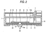
- Fig. 2 shows an A-A cross-sectional view of Fig. 1 in a state in which the thickness detecting sensor 100 is assembled.
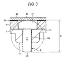
- Fig. 3 shows an enlarged view near a plunger 2 attached to a case 1.
- Fig. 4 shows an enlarged perspective view of a fixing electrode plate 3.
- Fig. 5 shows an enlarged perspective view of a movable electrode plate 4 and an electrode pressing plate 5.
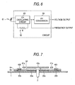
- Fig. 6 shows the construction of a converting circuit arranged in a circuit substrate 6.
- the thickness detecting sensor 100 in this embodiment mode is arranged near a medium conveying path 90 of a paper sheet kind processor 9 such as a copying machine, etc., and is arranged so as to be opposed to a guide plate 91, etc.
- a fixing electrode 30, a movable electrode 40 and the circuit substrate 6 are arranged within the case main body constructed by the case 1 and a shield plate 8.
- the fixing electrode 30 is arranged so as to fix the relative position to the medium conveying path 90.
- the movable electrode 40 is arranged so as to change the gap between the movable electrode 40 and this fixing electrode 30.
- the circuit substrate 6 has the converting circuit for converting electrostatic capacity stored between the fixing electrode 30 and the movable electrode 40 into an electric signal.
- the plunger 2 advanced and retreated in the axial direction by coming in contact with a medium is arranged in the thickness detecting sensor 100.
- a plunger insertion hole 31 is arranged at the center of the fixing electrode 30 and the plunger 2 is attached so as to be advanced and retreated.
- the rear end portion 21 of the plunger 2 comes in contact with the electrode face on the gap side in the movable electrode 40.
- the gap between the movable electrode 40 and the fixing electrode 30 is enlarged.
- a hemispherical projecting portion 12 (see Figs. 2 and 3) for projecting the tip portion 20 of the plunger 2 is arranged in the case 1.
- a through hole 12a extended through the inside of the case 1 is arranged in the central portion of this projecting portion 12 and the plunger 2 is held so as to be advanced and retreated.
- Fig. 3 shows an enlarged cross-sectional view of this plunger 2 and the case 1 near this plunger 2.
- This plunger 2 is formed in a columnar shape by resin.
- a contact portion of the plunger 2 with the medium is set to the tip portion 20 and a contact portion of the plunger 2 with the movable electrode 40 is set to the rear end portion 21, a head portion 22 larger in diameter than the tip portion 20 side and the through hole 12a of the case 1 is arranged on the rear end portion 21 side.
- This head portion 22 is abutted on a bottom face portion 11 inside the case 1.
- the plunger 2 is pulled and drops from the through hole 12a.
- the clearance of the through hole 12a is covered with the head portion 22 so as to prevent the invasion of dust, etc.
- the tip portion 20 and the rear end portion 21 of this plunger 2 are formed so as to construct the spherical surface of the same circle with the center of the plunger 2 in its longitudinal direction as a central point O.
- the plunger 2 is normally inclined by the clearance of the through hole 12a and the plunger 2 as shown by the broken line of Fig. 3.
- the tip portion 20 and the rear end portion 21 are formed on the spherical surface of the same circle in this way, the vertical distance B between the tip portion 20 and the rear end portion 21 of the plunger 2 is not changed so much even when the plunger 2 is inclined. Therefore, the displacement of the movable electrode 40 based on the inclination of the plunger 2 can be prevented as much as possible.
- a guide 13 for guiding the attachment of the fixing electrode plate 3 and the circuit substrate 6, the fixing electrode plate 3 having the fixing electrode 30, the movable electrode plate 4 having the movable electrode 40, and a pin 14 for fixing the electrode pressing plate 5 are arranged inside this case 1.
- the guide 13 is constructed by projecting the inside wall face of the case 1 toward the inside in a longitudinal shape.
- a first guide 13d having a large thickness size is arranged on the bottom face portion 11 side of the case 1.
- a step difference portion 13m is arranged in the upper portion of the first guide 13d.
- a second guide 13u having a thickness size smaller than that of the first guide 13d is arranged on the side of an opening portion 10 from this step difference portion 13m.
- a concave portion 32 corresponding to this first guide 13d is arranged in the fixing electrode plate 3. This fixing electrode plate 3 is attached along this first guide 13d.
- a concave portion 60 corresponding to the second guide 13u is also arranged in the circuit substrate 6.
- This circuit substrate 6 is placed and attached onto the step difference portion 13m along the second guide 13u. Further, the pin 14 is arranged so as to rise from the bottom face portion 11 of the case 1. In accordance with this, hole portions 33, 43, 53 corresponding to this pin 14 are arranged in the fixing electrode plate 3, the movable electrode plate 4 and the electrode pressing plate 5. The pin 14 is inserted into the fixing electrode plate 3, the movable electrode plate 4 and the electrode pressing plate 5, and the upper end portion of this pin 14 is deformed by heat, etc. and is fixed.
- the fixing electrode plate 3 is constructed by a printed board.
- the circular fixing electrode 30 arranged at the center, a resist 34 as an insulator, and a joining portion 35 for exposing a conductor to the surface are arranged.
- This fixing electrode 30 is covered with the resist 34 and functions as a dielectric between the fixing electrode 30 and the movable electrode 40.
- the joining portion 35 is an outer circumferential portion of the fixing electrode 30 and is arranged on the upper face of the resist 34. The joining portion 35 is then electrically connected to the movable electrode plate 4 closely attached to this fixing electrode plate 3.
- the fixing electrode 30 and the joining portion 35 are connected to terminals 37a, 37b, 37c through a line path 36, and are connected to terminals 67a, 67b, 67c (Fig. 1) of the circuit substrate 6 through an unillustrated lead wire, etc.
- a member shown by a broken line in Fig. 4 is located on the lower side of the resist 34, and only the joining portion 35 and the terminals 37a, 37b, 37c are exposed to the upper face of the resist 34.
- the plunger insertion hole 31 for inserting the plunger 2 is arranged in the central portion of this fixing electrode plate 3.
- This plunger insertion hole 31 has a diameter slightly larger than that of the head portion 22 of the plunger 2, and the plunger 2 is held by the through hole 12a arranged in the case 1 and this plunger insertion hole 31 such that the plunger 2 can be advanced and retreated.
- Fig. 5 shows the construction of the movable electrode plate 4.
- the movable electrode plate 4 is constructed by a thin metallic plate of a square shape, and the circular movable electrode 40 is arranged on the central side of a spring portion 41 of a linear shape.
- This spring portion 41 is constructed by a member left between plural slits 42 arranged in the movable electrode plate 4.
- plural slits 42 of a crank shape are arranged on the concentric circle, and the spring portion 41 is constructed by the member left between these slits 42.
- the movable electrode 40 is twisted and displaced by flexing this spring portion 41 while maintaining a plane state.
- This movable electrode 40 is arranged in the position opposed to the fixing electrode 30 in the attaching state of the movable electrode plate 4.
- An outer circumferential portion 44 pressed by the electrode pressing plate 5 is arranged outside this movable electrode 40.
- This electrode pressing plate 5 is constructed by a metallic plate of a square shape having the same outer shape size as the movable electrode plate 4, and has a circular window portion 50 for allowing the displacement of the movable electrode 40.
- This electrode pressing plate 5 is similarly attached to the pin 14 rising from the bottom face portion 11 of the case 1. While the electrode pressing plate 5 allows the displacement of the movable electrode 40 within the window portion 50, the electrode pressing plate 5 presses the outer circumferential portion 44 of the movable electrode plate 4 so that the joining portion 35 of the fixing electrode plate 3 and the outer circumferential portion 44 of the movable electrode plate 4 come in contact with a conductor.
- the terminals 67a, 67b, 67c connected to the terminals 37a, 37b, 37c of the fixing electrode plate 3 by an unillustrated lead wire, and a converting circuit for converting electrostatic capacity stored between the fixing electrode 30 and the movable electrode 40 into an electric signal are arranged in the circuit substrate 6.
- the construction of this converting circuit is shown in Fig. 6.
- reference numeral 61 designates a variable capacitor constructed by the fixing electrode 30 and the movable electrode 40.
- Reference numerals 62 and 63 respectively designate a resistance element and a CR oscillating circuit.
- reference numeral 64 designates an FV converting circuit for converting the electrostatic capacity into the electric signal.
- the circuit shown by the broken line in this Fig. 6 is arranged in the circuit substrate 6.
- the electrostatic capacity stored between the fixing electrode 30 and the movable electrode 40 by this circuit is converted into a frequency signal by the CR oscillating circuit 63, or is converted into a voltage by the FV converting circuit 64.
- These frequency signal and voltage are suitably selected and outputted in accordance with applications.
- a connector 7 (Fig. 1) outputs the electric signal such as these frequency signal and voltage, etc., and is fixed and attached to the circuit substrate 6.
- conveyance control of the medium, etc. based on this electric signal are performed by the paper sheet kind processor 9 such as a copying machine, etc.
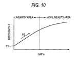
- the movable electrode 40 comes in close contact with the resist 34 of the fixing electrode plate 3 by the elastic force of the spring portion 41 arranged in the outer circumferential portion of the movable electrode 40. Since the resist 34 has a thin thickness of about several ⁇ m (about 20 ⁇ m) , the frequency outputted by the CR oscillating circuit 63 shows a minimum value in this state as shown by point P1 of Fig. 10.
- the central portion of the movable electrode 40 is pushed up by the rear end portion 21 of this plunger 2 and the gap between the movable electrode 40 and the fixing electrode 30 is changed so as to be enlarged.
- the frequency outputted by the CR oscillating circuit 63 is gradually increased as shown by the arrow P2 of Fig. 10.
- the fixing electrode 30 and the movable electrode 40 come in close contact with each other through the resist 34 in the initial state. Therefore, the frequency is linearly changed even when the gap is enlarged from this close contact.
- the change in the thickness of the medium can be exactly detected by detecting this frequency.
- the thickness detecting sensor has the fixing electrode 30 and the movable electrode 40 arranged so as to be opposed to each other, the plunger 2 for changing the gap between the electrodes by coming in contact with the medium, and the CR oscillating circuit 63 and the FV converting circuit 64 for converting the electrostatic capacity stored between the electrodes into the electric signal for detecting the thickness of the medium.
- the thickness detecting sensor is constructed such that the rear end portion 21 of the plunger 2 comes in contact with the electrode face of the gap side of the movable electrode 40, and the movable electrode 40 is displaced in the direction separated from the fixing electrode 30 correspondingly to the increase in the thickness of the medium. Accordingly, the frequency can be detected within an area in which this frequency is linearly changed. Thus, the thickness of the medium can be exactly detected. Further, since the movable electrode 40 is displaced in the direction separated from the fixing electrode 30, no dynamic range is limited by the gap set in the initial state and the dynamic range can be widely secured.
- the fixing electrode plate 3 is formed by a printed board, the terminals 37a, 37b, 37c and the line path 36 can be formed simultaneously with the fixing electrode 30 so that the fixing electrode, etc. can be simply made.
- the resist 34 is arranged on the fixing electrode 30 and the movable electrode 40 comes in close contact with the upper face of this resist 34. Accordingly, this resist 34 can be used as an original insulation protecting material, and can be also used as a dielectric. Accordingly, it is not necessary to separately newly arrange the dielectric between the electrodes.
- the shapes of the tip portion 20 and the rear end portion 21 of the plunger 2 are constructed in a spherical surface shape. Even when the plunger 2 is inclined by coming in contact with the medium, no vertical distance between the tip portion 20 and the rear end portion 21 of this plunger 2 is changed so much. Accordingly, the thickness detecting sensor reduces that a displacement error due to this inclination is applied to the movable electrode 40.
- the present invention is not limited to the above embodiment mode, but can be embodied in various modes.
- a pair of electrodes for invariably setting the gap between the electrodes may be also arranged in addition to the above embodiment mode.
- Fig. 7 shows the construction of a thickness detecting sensor in this second embodiment mode.
- a fixing electrode plate 3a, a movable electrode plate 4a, etc. are schematically shown in this Fig. 7.
- Reference numerals 30a, 30b designate two fixing electrodes respectively independently arranged on a printed board.
- Reference numeral 34 designates a resist arranged on these fixing electrodes 30a, 30b.
- Reference numeral 40a designates a movable electrode of the movable electrode plate 4a.
- Reference numeral 40b designates a fixing electrode of the movable electrode plate 4a.
- Reference numeral 41a designates a spring portion arranged in the outer circumferential portion of the movable electrode 40a.
- the fixing electrode 30a of the fixing electrode plate 3a side and the movable electrode 40a of the movable electrode plate 4a side are oppositely arranged, and the gap is enlarged by pressing the plunger 2.
- the fixing electrode 30b of the fixing electrode plate 3a side and the fixing electrode 40b of the movable electrode plate 4a side are oppositely arranged and are connected to the converting circuit shown by the broken line of Fig. 8 through respective unillustrated terminals.
- reference numeral 61a designates a variable capacitor constructed by the fixing electrode 30a of the fixing electrode plate 3a side and the movable electrode 40a of the movable electrode plate 4a side.
- Reference numeral 61b designates a capacitor constructed by the fixing electrode 30b of the fixing electrode plate 3a side and the fixing electrode 40b of the movable electrode plate 4a side.
- the electrostatic capacity stored onto the capacitor 61a side is changed by the pressed pressure of the plunger 2 based on the thickness of a medium and a change in environment. Further, the electrostatic capacity stored onto the capacitor 61b side is changed by only the change in environment.
- These electrostatic capacities are converted into frequency signals by CR oscillating circuits 63a, 63b and are outputted to counters 65a, 65b and their respective output values are differentiated by a CPU 66.
- a structure for canceling the expansion of a member based on the temperature change may be constructed as follows.
- Fig. 9 shows the construction of the thickness detecting sensor in this third embodiment mode.
- Fig. 9 shows the principle view of the thickness detecting sensor constructed so as not to cause a change in the gap on the basis of expansion of the member even when the member is expanded on the basis of the temperature change.
- reference numerals 1a and 2a respectively designate a case and a plunger. The other constructions are similar to those in the first or second embodiment mode.
- the plunger 2a and the case 1a are constructed by members having the same coefficient of linear expansion.
- the distances have the same length and the plunger 2a and the case 1a have the same coefficient of linear expansion. Therefore, no distance between the lower end face 15 of the case 1 and the tip portion 20a of the plunger 2 is changed even when the temperature change is caused. Thus, it is possible to cancel the expansion of the member based on the temperature change.
- the plunger insertion hole 31 is arranged in the central portion of the fixing electrode 30, and the movable electrode 40 is pressed by the rear end portion 22 of the plunger 2 from the electrode face of the gap side.
- the thickness detecting sensor can be also constructed such that the plunger is connected to the outer circumferential portion of the movable electrode by passing through the outside of the fixing electrode plate and the movable electrode is raised from the upper side without arranging the plunger insertion hole 31 in this way.
- one electrode is set to the fixing electrode and the other electrode is set to the movable electrode.
- each of the electrodes can be also movably constructed if the thickness detecting sensor is constructed such that the gap is enlarged by making the electrode come in contact with the medium.
- the thickness detecting sensor has a pair of electrodes arranged so as to be opposed to each other, a plunger for changing the gap between the electrodes by coming in contact with a medium, and a converting circuit for converting electrostatic capacity stored between the electrodes into an electric signal.
- the gap between the above electrodes is enlarged by displacement of the plunger corresponding to an increase in the thickness of the medium.
- the opposed electrodes in the initial state can be arranged so as to come in close contact with each other.
- frequency can be exactly detected within an area for linearly changing this frequency even when the gap between the electrodes is enlarged correspondingly to the increase in the thickness of the medium.
- no dynamic range is determined by the gap in the initial state, and the dynamic range can be widely secured.
Landscapes
- Engineering & Computer Science (AREA)
- General Engineering & Computer Science (AREA)
- Physics & Mathematics (AREA)
- General Physics & Mathematics (AREA)
- Measurement Of Length, Angles, Or The Like Using Electric Or Magnetic Means (AREA)
- A Measuring Device Byusing Mechanical Method (AREA)
Abstract
Description
- The present invention relates to a thickness detecting sensor for detecting the thickness of a medium of a thin paper sheet shape such as a sheet of paper for a copy, an OHP film, a banknote, etc., and more concretely relates to a thickness detecting sensor able to detect the thickness of the medium correspondingly to electrostatic capacity stored between electrodes by changing the gap between these electrodes correspondingly to the thickness of the medium.
- The thickness detecting sensor for detecting the thickness of the medium is arranged in a copying machine, etc. in recent years. This thickness detecting sensor generally detects whether paper sheets sequentially sent out of a cartridge, etc. are overlapped or not. When the thickness detecting sensor detects a predetermined thickness or more, the thickness detecting sensor judges that it is the overlap sending, and stops the conveyance, etc. With respect to a sensor for detecting a contact state of the medium by coming in contact with this medium, a sensor disclosed in
patent literature 1 is known. - This sensor is constructed by arranging a fixing electrode arranged in a base film and a movable electrode arranged so as to be opposed to this fixing electrode. The movable electrode is displaced onto the fixing electrode side by making the medium come in contact with a member arranged on the movable electrode side. The contact state with the medium is detected on the basis of a change in electrostatic capacity caused by changing the gap between these electrodes.
- When the electrostatic capacity stored between the electrodes is detected, this electrostatic capacity is converted into a frequency signal by a CR oscillating circuit, etc., and this frequency is detected. However, with respect to the relation of this frequency and the gap between these electrodes, it is known that the relation as shown in Fig. 10 is formed. Namely, in a small area of the gap between the electrodes, the frequency is linearly changed correspondingly to an increase in the gap. In a large area of the gap between the electrodes, the frequency is only gradually changed even when the gap is increased. Therefore, when the gap is widely set in advance, there is a possibility that no frequency is linearly changed even when the gap is changed. Therefore, it is difficult to exactly detect the change in frequency. On the other hand, when the gap is narrowly set in advance, the frequency is linearly changed correspondingly to the change in the gap. Therefore, it is possible to exactly detect the change in frequency. However, when the gap is narrowly set in this way, the movable electrode can be displaced on the fixing electrode side only within the gap range. Therefore, when the medium having a thickness exceeding this gap range comes in contact with the sensor, this sensor is broken. Further, a dynamic range of the sensor is limited to the range of the gap between the electrodes so that the dynamic range is also reduced.
- Therefore, the present invention is made by noticing such problems, and its object is to provide a thickness detecting sensor able to largely set the dynamic range and exactly detect the thickness of the medium even when the dynamic range is largely set in this way.
- Namely, to solve the above problems, the thickness detecting sensor of the present invention comprises a pair of electrodes arranged so as to be opposed to each other, a plunger for changing the gap between the electrodes by coming in contact with a medium, and a converting circuit for converting electrostatic capacity stored between the electrodes into an electric signal, wherein the thickness detecting sensor is constructed such that the gap between the electrodes is enlarged by displacement of the plunger corresponding to an increase in the thickness of the medium.
- In accordance with such a construction, the electrodes oppositely arranged in the initial state (a state in which no medium comes in contact with the plunger) can approximately come in close contact with each other. Accordingly, even when the gap between the electrodes is enlarged by coming in contact with the medium, its frequency can be detected within an area in which the frequency is linearly changed. Further, since the electrodes are displaced in the widening direction of the gap, there is no case in which the dynamic range is determined by the gap set in the initial state as in the conventional case. Thus, the dynamic range can be widely secured as much as possible.
- Further, in another embodiment mode, one of the electrodes is set to a fixing electrode and a variable electrode for changing the gap by coming in contact with the medium and a fixing electrode for maintaining the gap are arranged on the side opposed to this set fixing electrode.
- The electrostatic capacity stored between the electrodes is normally changed by the temperature of the external air, a moisture containing amount, etc. Therefore, the electrostatic capacity is changed by influences such as the temperature of the external air, the moisture containing amount, etc. Accordingly, there is a possibility that an incorrect detecting result is outputted. Therefore, the fixing electrode is arranged and the movable electrode and another fixing electrode are arranged on the side opposed to the fixing electrode. The frequencies are calculated on the basis of the electrostatic capacity stored onto this movable electrode side and the electrostatic capacity stored between both the fixing electrodes. The influences such as temperature, etc. are canceled by calculating the difference between these frequencies.
- Further, in a preferable embodiment mode of the present invention, the thickness detecting sensor comprises a fixing electrode arranged so as to fix the relative position to a medium conveying path, a movable electrode arranged so as to be opposed to this fixing electrode, a spring portion for displacing the movable electrode so as to change the gap between the fixing electrode and the movable electrode, a converting circuit for converting electrostatic capacity stored between the fixing electrode and the movable electrode into an electric signal, and a plunger advanced and retreated in the axial direction by coming in contact with a medium, wherein the thickness detecting sensor is constructed such that the plunger is attached so as to be advanced and retreated by arranging a plunger insertion hole in the fixing electrode and the gap is enlarged by pressing the electrode face of the gap side in the movable electrode by this plunger.
- In accordance with such a construction, since the movable electrode is pressed from the inside of the gap, the gap can be reliably enlarged by the simple construction.
- Further, in another embodiment mode, one fixing electrode constituting the pair of electrodes is constructed by a printed board.
- In accordance with such a construction, the fixing electrode, a line path, a terminal, etc. can be simultaneously printed, and the fixing electrode, etc. can be simply made.
- In addition, a resist is arranged on the fixing electrode made by this printed board, and the gap between the opposed electrodes is formed by this resist.
- In accordance with such a construction, it is not necessary to separately newly arrange a dielectric between the electrodes. Thus, in addition to the original function of the resist, this resist can be also used as the dielectric.
- Further, a head portion having a diameter larger than that of the tip portion of the plunger is arranged in the rear end portion of the plunger.
- In accordance with such a construction, when a through hole is formed in a case, etc. and its plunger is held, the through hole can be blocked by its head portion and the invasion of dust from the exterior can be prevented.
- Further, the tip portion and the rear end portion of the plunger are constructed in the shape of a spherical surface.
- In accordance with such a construction, even when the plunger is inclined by coming in contact with the medium, etc., its both end portions are formed in the spherical surface shape so that no distance between the tip portion and the rear end portion of the plunger in its longitudinal direction is changed. Therefore, even when the rear end portion of the plunger comes in contact with the electrode face of the gap side of the movable electrode and the movable electrode is displaced, no displacing amount of the movable electrode due to the inclination of the plunger is influenced.
-
- Fig. 1 is an exploded perspective view of a thickness detecting sensor in one embodiment mode of the present invention.
- Fig. 2 is an A-A cross-sectional view of Fig. 1 in a state in which the thickness detecting sensor in this embodiment mode is assembled.
- Fig. 3 is an enlarged view near a plunger in this embodiment mode.
- Fig. 4 is a perspective view of the external appearance of a fixing electrode plate in this embodiment mode.
- Fig. 5 is a perspective view of the external appearances of a movable electrode plate and an electrode pressing plate in this embodiment mode.
- Fig. 6 is a view showing a converting circuit arranged in a circuit substrate in this embodiment mode.
- Fig. 7 is a view showing the operating principles of a fixing electrode and a movable electrode in a second embodiment mode of the present invention.
- Fig. 8 is a circuit constructional view used in the second embodiment mode of the present invention.
- Fig. 9 is a principle view showing the constructions of a case and a plunger in a third embodiment mode of the present invention.
- Fig. 10 is a view showing the relation of frequency and the gap between the electrodes.
- Fig. 11 is a view showing a using state of the thickness detecting sensor of the present invention.
-
- The construction of a
thickness detecting sensor 100 in a first embodiment mode of the present invention will next be explained with reference to the drawings. In this embodiment mode, Fig. 1 shows an exploded perspective view of thethickness detecting sensor 100. Fig. 2 shows an A-A cross-sectional view of Fig. 1 in a state in which thethickness detecting sensor 100 is assembled. Fig. 3 shows an enlarged view near aplunger 2 attached to acase 1. Fig. 4 shows an enlarged perspective view of a fixingelectrode plate 3. Fig. 5 shows an enlarged perspective view of amovable electrode plate 4 and anelectrode pressing plate 5. Fig. 6 shows the construction of a converting circuit arranged in acircuit substrate 6. - As shown in Fig. 11, the
thickness detecting sensor 100 in this embodiment mode is arranged near a medium conveyingpath 90 of a paper sheet kind processor 9 such as a copying machine, etc., and is arranged so as to be opposed to aguide plate 91, etc. As shown in Fig. 1, in thisthickness detecting sensor 100, a fixingelectrode 30, amovable electrode 40 and thecircuit substrate 6 are arranged within the case main body constructed by thecase 1 and ashield plate 8. The fixingelectrode 30 is arranged so as to fix the relative position to the medium conveyingpath 90. Themovable electrode 40 is arranged so as to change the gap between themovable electrode 40 and this fixingelectrode 30. Thecircuit substrate 6 has the converting circuit for converting electrostatic capacity stored between the fixingelectrode 30 and themovable electrode 40 into an electric signal. Further, theplunger 2 advanced and retreated in the axial direction by coming in contact with a medium is arranged in thethickness detecting sensor 100. Aplunger insertion hole 31 is arranged at the center of the fixingelectrode 30 and theplunger 2 is attached so as to be advanced and retreated. Therear end portion 21 of theplunger 2 comes in contact with the electrode face on the gap side in themovable electrode 40. Thus, when the medium comes in contact with theplunger 2, the gap between themovable electrode 40 and the fixingelectrode 30 is enlarged. The construction of thisthickness detecting sensor 100 will next be explained in detail. - A hemispherical projecting portion 12 (see Figs. 2 and 3) for projecting the
tip portion 20 of theplunger 2 is arranged in thecase 1. A throughhole 12a extended through the inside of thecase 1 is arranged in the central portion of this projectingportion 12 and theplunger 2 is held so as to be advanced and retreated. - Fig. 3 shows an enlarged cross-sectional view of this
plunger 2 and thecase 1 near thisplunger 2. Thisplunger 2 is formed in a columnar shape by resin. When a contact portion of theplunger 2 with the medium is set to thetip portion 20 and a contact portion of theplunger 2 with themovable electrode 40 is set to therear end portion 21, ahead portion 22 larger in diameter than thetip portion 20 side and the throughhole 12a of thecase 1 is arranged on therear end portion 21 side. Thishead portion 22 is abutted on abottom face portion 11 inside thecase 1. Thus, it is prevented that theplunger 2 is pulled and drops from the throughhole 12a. Further, the clearance of the throughhole 12a is covered with thehead portion 22 so as to prevent the invasion of dust, etc. from the exterior. Thetip portion 20 and therear end portion 21 of thisplunger 2 are formed so as to construct the spherical surface of the same circle with the center of theplunger 2 in its longitudinal direction as a central point O. When thisplunger 2 comes in contact with the medium, theplunger 2 is normally inclined by the clearance of the throughhole 12a and theplunger 2 as shown by the broken line of Fig. 3. However, when thetip portion 20 and therear end portion 21 are formed on the spherical surface of the same circle in this way, the vertical distance B between thetip portion 20 and therear end portion 21 of theplunger 2 is not changed so much even when theplunger 2 is inclined. Therefore, the displacement of themovable electrode 40 based on the inclination of theplunger 2 can be prevented as much as possible. - On the other hand, as shown in Figs. 1 and 2, a
guide 13 for guiding the attachment of the fixingelectrode plate 3 and thecircuit substrate 6, the fixingelectrode plate 3 having the fixingelectrode 30, themovable electrode plate 4 having themovable electrode 40, and apin 14 for fixing theelectrode pressing plate 5 are arranged inside thiscase 1. - The
guide 13 is constructed by projecting the inside wall face of thecase 1 toward the inside in a longitudinal shape. Afirst guide 13d having a large thickness size is arranged on thebottom face portion 11 side of thecase 1. Further, astep difference portion 13m is arranged in the upper portion of thefirst guide 13d. Further, asecond guide 13u having a thickness size smaller than that of thefirst guide 13d is arranged on the side of anopening portion 10 from thisstep difference portion 13m. Aconcave portion 32 corresponding to thisfirst guide 13d is arranged in the fixingelectrode plate 3. This fixingelectrode plate 3 is attached along thisfirst guide 13d. Further, aconcave portion 60 corresponding to thesecond guide 13u is also arranged in thecircuit substrate 6. Thiscircuit substrate 6 is placed and attached onto thestep difference portion 13m along thesecond guide 13u. Further, thepin 14 is arranged so as to rise from thebottom face portion 11 of thecase 1. In accordance with this,hole portions pin 14 are arranged in the fixingelectrode plate 3, themovable electrode plate 4 and theelectrode pressing plate 5. Thepin 14 is inserted into the fixingelectrode plate 3, themovable electrode plate 4 and theelectrode pressing plate 5, and the upper end portion of thispin 14 is deformed by heat, etc. and is fixed. - Next, the construction of the fixing
electrode plate 3 is shown in Fig. 4, etc. The fixingelectrode plate 3 is constructed by a printed board. In the fixingelectrode plate 3, thecircular fixing electrode 30 arranged at the center, a resist 34 as an insulator, and a joiningportion 35 for exposing a conductor to the surface are arranged. This fixingelectrode 30 is covered with the resist 34 and functions as a dielectric between the fixingelectrode 30 and themovable electrode 40. On the other hand, the joiningportion 35 is an outer circumferential portion of the fixingelectrode 30 and is arranged on the upper face of the resist 34. The joiningportion 35 is then electrically connected to themovable electrode plate 4 closely attached to this fixingelectrode plate 3. The fixingelectrode 30 and the joiningportion 35 are connected toterminals line path 36, and are connected toterminals circuit substrate 6 through an unillustrated lead wire, etc. A member shown by a broken line in Fig. 4 is located on the lower side of the resist 34, and only the joiningportion 35 and theterminals plunger insertion hole 31 for inserting theplunger 2 is arranged in the central portion of this fixingelectrode plate 3. Thisplunger insertion hole 31 has a diameter slightly larger than that of thehead portion 22 of theplunger 2, and theplunger 2 is held by the throughhole 12a arranged in thecase 1 and thisplunger insertion hole 31 such that theplunger 2 can be advanced and retreated. - Fig. 5 shows the construction of the
movable electrode plate 4. Themovable electrode plate 4 is constructed by a thin metallic plate of a square shape, and the circularmovable electrode 40 is arranged on the central side of aspring portion 41 of a linear shape. Thisspring portion 41 is constructed by a member left betweenplural slits 42 arranged in themovable electrode plate 4. In this embodiment mode,plural slits 42 of a crank shape are arranged on the concentric circle, and thespring portion 41 is constructed by the member left between theseslits 42. Themovable electrode 40 is twisted and displaced by flexing thisspring portion 41 while maintaining a plane state. Thismovable electrode 40 is arranged in the position opposed to the fixingelectrode 30 in the attaching state of themovable electrode plate 4. An outercircumferential portion 44 pressed by theelectrode pressing plate 5 is arranged outside thismovable electrode 40. - This
electrode pressing plate 5 is constructed by a metallic plate of a square shape having the same outer shape size as themovable electrode plate 4, and has acircular window portion 50 for allowing the displacement of themovable electrode 40. Thiselectrode pressing plate 5 is similarly attached to thepin 14 rising from thebottom face portion 11 of thecase 1. While theelectrode pressing plate 5 allows the displacement of themovable electrode 40 within thewindow portion 50, theelectrode pressing plate 5 presses the outercircumferential portion 44 of themovable electrode plate 4 so that the joiningportion 35 of the fixingelectrode plate 3 and the outercircumferential portion 44 of themovable electrode plate 4 come in contact with a conductor. - As shown in Fig. 1, the
terminals terminals electrode plate 3 by an unillustrated lead wire, and a converting circuit for converting electrostatic capacity stored between the fixingelectrode 30 and themovable electrode 40 into an electric signal are arranged in thecircuit substrate 6. The construction of this converting circuit is shown in Fig. 6. - In Fig. 6,
reference numeral 61 designates a variable capacitor constructed by the fixingelectrode 30 and themovable electrode 40.Reference numerals reference numeral 64 designates an FV converting circuit for converting the electrostatic capacity into the electric signal. The circuit shown by the broken line in this Fig. 6 is arranged in thecircuit substrate 6. The electrostatic capacity stored between the fixingelectrode 30 and themovable electrode 40 by this circuit is converted into a frequency signal by theCR oscillating circuit 63, or is converted into a voltage by theFV converting circuit 64. These frequency signal and voltage are suitably selected and outputted in accordance with applications. - A connector 7 (Fig. 1) outputs the electric signal such as these frequency signal and voltage, etc., and is fixed and attached to the
circuit substrate 6. Thus, conveyance control of the medium, etc. based on this electric signal are performed by the paper sheet kind processor 9 such as a copying machine, etc. - The operating principle of the
thickness detecting sensor 100 constructed in this way will next be explained. - First, in a state in which no medium exists, the
movable electrode 40 comes in close contact with the resist 34 of the fixingelectrode plate 3 by the elastic force of thespring portion 41 arranged in the outer circumferential portion of themovable electrode 40. Since the resist 34 has a thin thickness of about several µm (about 20 µm) , the frequency outputted by theCR oscillating circuit 63 shows a minimum value in this state as shown by point P1 of Fig. 10. When the conveyed medium comes in contact with theplunger 2 and pushes up theplunger 2 by its increasing thickness amount, the central portion of themovable electrode 40 is pushed up by therear end portion 21 of thisplunger 2 and the gap between themovable electrode 40 and the fixingelectrode 30 is changed so as to be enlarged. At this time, the frequency outputted by theCR oscillating circuit 63 is gradually increased as shown by the arrow P2 of Fig. 10. However, in this embodiment mode, the fixingelectrode 30 and themovable electrode 40 come in close contact with each other through the resist 34 in the initial state. Therefore, the frequency is linearly changed even when the gap is enlarged from this close contact. Thus, the change in the thickness of the medium can be exactly detected by detecting this frequency. - Thus, in the above embodiment mode, the thickness detecting sensor has the fixing
electrode 30 and themovable electrode 40 arranged so as to be opposed to each other, theplunger 2 for changing the gap between the electrodes by coming in contact with the medium, and theCR oscillating circuit 63 and theFV converting circuit 64 for converting the electrostatic capacity stored between the electrodes into the electric signal for detecting the thickness of the medium. The thickness detecting sensor is constructed such that therear end portion 21 of theplunger 2 comes in contact with the electrode face of the gap side of themovable electrode 40, and themovable electrode 40 is displaced in the direction separated from the fixingelectrode 30 correspondingly to the increase in the thickness of the medium. Accordingly, the frequency can be detected within an area in which this frequency is linearly changed. Thus, the thickness of the medium can be exactly detected. Further, since themovable electrode 40 is displaced in the direction separated from the fixingelectrode 30, no dynamic range is limited by the gap set in the initial state and the dynamic range can be widely secured. - Further, in this embodiment mode, since the fixing
electrode plate 3 is formed by a printed board, theterminals line path 36 can be formed simultaneously with the fixingelectrode 30 so that the fixing electrode, etc. can be simply made. - Further, the resist 34 is arranged on the fixing
electrode 30 and themovable electrode 40 comes in close contact with the upper face of this resist 34. Accordingly, this resist 34 can be used as an original insulation protecting material, and can be also used as a dielectric. Accordingly, it is not necessary to separately newly arrange the dielectric between the electrodes. - In addition, the shapes of the
tip portion 20 and therear end portion 21 of theplunger 2 are constructed in a spherical surface shape. Even when theplunger 2 is inclined by coming in contact with the medium, no vertical distance between thetip portion 20 and therear end portion 21 of thisplunger 2 is changed so much. Accordingly, the thickness detecting sensor reduces that a displacement error due to this inclination is applied to themovable electrode 40. - The present invention is not limited to the above embodiment mode, but can be embodied in various modes.
- For example, when the error of the electrostatic capacity due to temperature characteristics, etc. is removed, a pair of electrodes for invariably setting the gap between the electrodes may be also arranged in addition to the above embodiment mode.
- Fig. 7 shows the construction of a thickness detecting sensor in this second embodiment mode. A fixing
electrode plate 3a, amovable electrode plate 4a, etc. are schematically shown in this Fig. 7.Reference numerals Reference numeral 34 designates a resist arranged on these fixingelectrodes Reference numeral 40a designates a movable electrode of themovable electrode plate 4a.Reference numeral 40b designates a fixing electrode of themovable electrode plate 4a.Reference numeral 41a designates a spring portion arranged in the outer circumferential portion of themovable electrode 40a. The fixingelectrode 30a of the fixingelectrode plate 3a side and themovable electrode 40a of themovable electrode plate 4a side are oppositely arranged, and the gap is enlarged by pressing theplunger 2. Independently of this structure, the fixingelectrode 30b of the fixingelectrode plate 3a side and the fixingelectrode 40b of themovable electrode plate 4a side are oppositely arranged and are connected to the converting circuit shown by the broken line of Fig. 8 through respective unillustrated terminals. - In Fig. 8,
reference numeral 61a designates a variable capacitor constructed by the fixingelectrode 30a of the fixingelectrode plate 3a side and themovable electrode 40a of themovable electrode plate 4a side.Reference numeral 61b designates a capacitor constructed by the fixingelectrode 30b of the fixingelectrode plate 3a side and the fixingelectrode 40b of themovable electrode plate 4a side. The electrostatic capacity stored onto thecapacitor 61a side is changed by the pressed pressure of theplunger 2 based on the thickness of a medium and a change in environment. Further, the electrostatic capacity stored onto thecapacitor 61b side is changed by only the change in environment. These electrostatic capacities are converted into frequency signals byCR oscillating circuits counters CPU 66. - In accordance with such a construction, it is possible to cancel the change in the electrostatic capacity due to a change in temperature, etc. and detect the exact thickness not depending on the change in temperature, etc.
- Further, a structure for canceling the expansion of a member based on the temperature change may be constructed as follows.
- Fig. 9 shows the construction of the thickness detecting sensor in this third embodiment mode. Fig. 9 shows the principle view of the thickness detecting sensor constructed so as not to cause a change in the gap on the basis of expansion of the member even when the member is expanded on the basis of the temperature change. In Fig. 9,
reference numerals plunger 2a and thecase 1a are constructed by members having the same coefficient of linear expansion. When the distance from thelower face 22d of ahead portion 22a in theplunger 2a to thelower end face 15 of thecase 1a is set to A and the distance from therear end portion 21a of theplunger 2a to thetip portion 20a is set to B, the thickness detecting sensor is constructed so as to form "A=B". In accordance with such a construction, the distances have the same length and theplunger 2a and thecase 1a have the same coefficient of linear expansion. Therefore, no distance between thelower end face 15 of thecase 1 and thetip portion 20a of theplunger 2 is changed even when the temperature change is caused. Thus, it is possible to cancel the expansion of the member based on the temperature change. - Further, in the first embodiment mode, the
plunger insertion hole 31 is arranged in the central portion of the fixingelectrode 30, and themovable electrode 40 is pressed by therear end portion 22 of theplunger 2 from the electrode face of the gap side. However, the thickness detecting sensor can be also constructed such that the plunger is connected to the outer circumferential portion of the movable electrode by passing through the outside of the fixing electrode plate and the movable electrode is raised from the upper side without arranging theplunger insertion hole 31 in this way. - Further, in the above embodiment mode, one electrode is set to the fixing electrode and the other electrode is set to the movable electrode. However, each of the electrodes can be also movably constructed if the thickness detecting sensor is constructed such that the gap is enlarged by making the electrode come in contact with the medium.
- The thickness detecting sensor has a pair of electrodes arranged so as to be opposed to each other, a plunger for changing the gap between the electrodes by coming in contact with a medium, and a converting circuit for converting electrostatic capacity stored between the electrodes into an electric signal. In the thickness detecting sensor, the gap between the above electrodes is enlarged by displacement of the plunger corresponding to an increase in the thickness of the medium. Accordingly, the opposed electrodes in the initial state can be arranged so as to come in close contact with each other. Thus, frequency can be exactly detected within an area for linearly changing this frequency even when the gap between the electrodes is enlarged correspondingly to the increase in the thickness of the medium. Further, no dynamic range is determined by the gap in the initial state, and the dynamic range can be widely secured.
Claims (8)
- A thickness detecting sensor comprising a pair of electrodes arranged so as to be opposed to each other, a plunger for changing the gap between the electrodes by coming in contact with a medium, and a converting circuit for converting electrostatic capacity stored between the electrodes into an electric signal,
wherein the thickness detecting sensor is constructed such that the gap between said electrodes is enlarged by displacement of the plunger corresponding to an increase in the thickness of the medium. - The thickness detecting sensor according to claim 1, wherein one of said electrodes is set to a fixing electrode and a variable electrode for changing the gap by coming in contact with the medium and a fixing electrode for maintaining the gap are arranged on the side opposed to this set fixing electrode.
- A thickness detecting sensor comprising a fixing electrode arranged so as to fix the relative position to a medium conveying path, a movable electrode arranged so as to be opposed to this fixing electrode, a spring portion for displacing the movable electrode so as to change the gap between said fixing electrode and the movable electrode, a converting circuit for converting electrostatic capacity stored between said fixing electrode and said movable electrode into an electric signal, and a plunger advanced and retreated in the axial direction by coming in contact with a medium, wherein the thickness detecting sensor is constructed such that the plunger is attached so as to be advanced and retreated by arranging a plunger insertion hole in said fixing electrode and the gap is enlarged by pressing the electrode face of the gap side in the movable electrode by the plunger.
- The thickness detecting sensor according to claim 1 or 3, wherein one fixing electrode constituting said pair of electrodes is made by a printed board.
- The thickness detecting sensor according to claim 4, wherein a resist is arranged on the fixing electrode made by said printed board, and the gap between the opposed electrodes is formed by this resist.
- The thickness detecting sensor according to claim 1 or 3, wherein a head portion having a diameter larger than that of the tip portion of the plunger is arranged in the rear end portion of the plunger.
- The thickness detecting sensor according to claim 1 or 3, wherein the tip portion and the rear end portion of said plunger are constructed in the shape of a spherical surface.
- The thickness detecting sensor according to claim 1 or 3, wherein a case for holding the plunger so as to be advanced and retreated is further arranged, and this case and the plunger are formed by the same material, and the distance from a plunger placing face to the lower end face in the case and the length of the plunger are set to the same.
Applications Claiming Priority (2)
| Application Number | Priority Date | Filing Date | Title |
|---|---|---|---|
| JP2003136875 | 2003-05-15 | ||
| JP2003136875A JP4029770B2 (en) | 2003-05-15 | 2003-05-15 | Thickness detection sensor |
Publications (2)
| Publication Number | Publication Date |
|---|---|
| EP1480003A1 true EP1480003A1 (en) | 2004-11-24 |
| EP1480003B1 EP1480003B1 (en) | 2015-02-18 |
Family
ID=33095367
Family Applications (1)
| Application Number | Title | Priority Date | Filing Date |
|---|---|---|---|
| EP04008505.2A Expired - Lifetime EP1480003B1 (en) | 2003-05-15 | 2004-04-07 | Thickness detecting sensor |
Country Status (6)
| Country | Link |
|---|---|
| US (1) | US7019539B2 (en) |
| EP (1) | EP1480003B1 (en) |
| JP (1) | JP4029770B2 (en) |
| KR (1) | KR100785556B1 (en) |
| CN (1) | CN100416217C (en) |
| TW (1) | TWI235820B (en) |
Families Citing this family (8)
| Publication number | Priority date | Publication date | Assignee | Title |
|---|---|---|---|---|
| JP4189426B2 (en) * | 2007-01-31 | 2008-12-03 | 株式会社東芝 | Sensor device, and portable communication terminal and electronic device using the same |
| JP5162257B2 (en) * | 2008-01-09 | 2013-03-13 | 株式会社ミツトヨ | Contact uniaxial displacement sensor |
| US8638109B2 (en) * | 2009-12-31 | 2014-01-28 | Mapper Lithography Ip B.V. | Capacitive sensing system with differential pairs |
| CN103925867A (en) * | 2014-04-29 | 2014-07-16 | 威海华菱光电股份有限公司 | Thickness sensor and thickness measuring method |
| CN104390580B (en) * | 2014-12-04 | 2018-06-22 | 上海集成电路研发中心有限公司 | Metal film film thickness measurement system and the method that film thickness measurement is carried out using the system |
| CN105674845A (en) * | 2016-02-17 | 2016-06-15 | 西南交通大学 | Penetrating-type quick measurement device for on-site measurement of thickness of waterproof film sprayed on hard base plane |
| CN106017296B (en) * | 2016-08-09 | 2020-09-25 | 爱德森(厦门)电子有限公司 | Method for measuring thickness of covering layer on surface of conductive material substrate with uneven conductivity |
| CN107448867B (en) * | 2017-09-20 | 2023-08-29 | 华域视觉科技(上海)有限公司 | ADB module |
Citations (5)
| Publication number | Priority date | Publication date | Assignee | Title |
|---|---|---|---|---|
| US4320667A (en) * | 1978-10-17 | 1982-03-23 | Lucas Industries Limited | Load transducer |
| US5531434A (en) * | 1994-12-05 | 1996-07-02 | Hewlett-Packard Company | Multiple page sensor for automatic document feeder |
| WO1997022845A1 (en) * | 1995-12-20 | 1997-06-26 | Hysitron, Incorporated | Multi-dimensional capacitive transducer |
| US20020039271A1 (en) * | 2000-09-29 | 2002-04-04 | Fournier John A. | Linear displacement sensor apparatus |
| JP2002149337A (en) * | 2000-11-13 | 2002-05-24 | Omron Corp | pointing device |
Family Cites Families (8)
| Publication number | Priority date | Publication date | Assignee | Title |
|---|---|---|---|---|
| JPS597649A (en) * | 1982-07-05 | 1984-01-14 | Fuji Photo Film Co Ltd | Sheet work conveying structure |
| JPH0789890B2 (en) * | 1991-04-19 | 1995-10-04 | 三菱化学株式会社 | Defoaming agent for beverage and beverage using the same |
| JPH05288619A (en) * | 1992-04-07 | 1993-11-02 | Youji Yamada | Capacitive tactile sensor |
| CN2160884Y (en) * | 1993-03-04 | 1994-04-06 | 石油大学(华东) | Sensors for magnetoelectric parallel non-magnetic plating and coating thickness gauges |
| JP3298328B2 (en) * | 1994-09-29 | 2002-07-02 | 株式会社豊田中央研究所 | Dielectric constant measuring device |
| JPH08292272A (en) * | 1995-04-24 | 1996-11-05 | Kanto Auto Works Ltd | Detecting device of overlapping plate |
| JP2001264050A (en) * | 2000-03-14 | 2001-09-26 | Mitsutoyo Corp | Minute shape measuring apparatus |
| US6388452B1 (en) * | 2000-04-20 | 2002-05-14 | Hewlett-Packard Company | Device for sensing media thickness using capacitance measurements |
-
2003
- 2003-05-15 JP JP2003136875A patent/JP4029770B2/en not_active Expired - Fee Related
-
2004
- 2004-04-07 EP EP04008505.2A patent/EP1480003B1/en not_active Expired - Lifetime
- 2004-04-23 KR KR1020040028177A patent/KR100785556B1/en not_active Expired - Fee Related
- 2004-05-11 CN CNB2004100445675A patent/CN100416217C/en not_active Expired - Fee Related
- 2004-05-11 US US10/843,002 patent/US7019539B2/en not_active Expired - Fee Related
- 2004-05-12 TW TW093113265A patent/TWI235820B/en not_active IP Right Cessation
Patent Citations (5)
| Publication number | Priority date | Publication date | Assignee | Title |
|---|---|---|---|---|
| US4320667A (en) * | 1978-10-17 | 1982-03-23 | Lucas Industries Limited | Load transducer |
| US5531434A (en) * | 1994-12-05 | 1996-07-02 | Hewlett-Packard Company | Multiple page sensor for automatic document feeder |
| WO1997022845A1 (en) * | 1995-12-20 | 1997-06-26 | Hysitron, Incorporated | Multi-dimensional capacitive transducer |
| US20020039271A1 (en) * | 2000-09-29 | 2002-04-04 | Fournier John A. | Linear displacement sensor apparatus |
| JP2002149337A (en) * | 2000-11-13 | 2002-05-24 | Omron Corp | pointing device |
Non-Patent Citations (1)
| Title |
|---|
| PATENT ABSTRACTS OF JAPAN vol. 2002, no. 09 4 September 2002 (2002-09-04) * |
Also Published As
| Publication number | Publication date |
|---|---|
| CN1550749A (en) | 2004-12-01 |
| JP4029770B2 (en) | 2008-01-09 |
| US20040227526A1 (en) | 2004-11-18 |
| KR20040098525A (en) | 2004-11-20 |
| TW200500592A (en) | 2005-01-01 |
| US7019539B2 (en) | 2006-03-28 |
| TWI235820B (en) | 2005-07-11 |
| JP2004340710A (en) | 2004-12-02 |
| EP1480003B1 (en) | 2015-02-18 |
| KR100785556B1 (en) | 2007-12-13 |
| CN100416217C (en) | 2008-09-03 |
Similar Documents
| Publication | Publication Date | Title |
|---|---|---|
| EP0542436B1 (en) | Accelerometer | |
| JP3648170B2 (en) | A device that detects the thickness of media by measuring volume | |
| US8763468B2 (en) | Electrode device, pressure sensor and pressure meter | |
| US7296473B2 (en) | Pressure sensor | |
| EP1480003B1 (en) | Thickness detecting sensor | |
| JP3601252B2 (en) | Knock sensor | |
| EP1840581A1 (en) | Capacitive sensor | |
| EP0294689B1 (en) | Hot film type air flow meter | |
| JP2000048694A (en) | Capacitive proximity sensor | |
| US20120289091A1 (en) | Sensor | |
| US6257068B1 (en) | Capacitive pressure sensor having petal electrodes | |
| CN108731850B (en) | Capacitive pressure sensor and electronic pen | |
| JP4910215B2 (en) | Variable capacitor, position indicator and coordinate input device | |
| JP6038551B2 (en) | Capacitor unit for voltage measuring equipment | |
| KR101998659B1 (en) | Capacitive force sensor switch with coil spring | |
| JPH0745919Y2 (en) | Electronic device housing structure | |
| CN120344846B (en) | Capacitive liquid sensor and method for mounting capacitive liquid sensor | |
| CN212991342U (en) | A conductive component | |
| KR20210004236A (en) | Sensor | |
| JP2011058889A (en) | Capacitance type pointing device | |
| JP2542222B2 (en) | Electrode configuration of capacitance level sensor | |
| EP4145858A1 (en) | Measuring pad | |
| JP2683367B2 (en) | Switches and switch covers | |
| JP6700142B2 (en) | Wiring connection structure and capacitance type input device | |
| JP4245747B2 (en) | Acceleration detector |
Legal Events
| Date | Code | Title | Description |
|---|---|---|---|
| PUAI | Public reference made under article 153(3) epc to a published international application that has entered the european phase |
Free format text: ORIGINAL CODE: 0009012 |
|
| AK | Designated contracting states |
Kind code of ref document: A1 Designated state(s): AT BE BG CH CY CZ DE DK EE ES FI FR GB GR HU IE IT LI LU MC NL PL PT RO SE SI SK TR |
|
| AX | Request for extension of the european patent |
Extension state: AL HR LT LV MK |
|
| 17P | Request for examination filed |
Effective date: 20050311 |
|
| AKX | Designation fees paid |
Designated state(s): DE FR GB |
|
| 17Q | First examination report despatched |
Effective date: 20110610 |
|
| GRAP | Despatch of communication of intention to grant a patent |
Free format text: ORIGINAL CODE: EPIDOSNIGR1 |
|
| INTG | Intention to grant announced |
Effective date: 20140813 |
|
| GRAS | Grant fee paid |
Free format text: ORIGINAL CODE: EPIDOSNIGR3 |
|
| GRAA | (expected) grant |
Free format text: ORIGINAL CODE: 0009210 |
|
| AK | Designated contracting states |
Kind code of ref document: B1 Designated state(s): DE FR GB |
|
| REG | Reference to a national code |
Ref country code: GB Ref legal event code: FG4D |
|
| REG | Reference to a national code |
Ref country code: DE Ref legal event code: R096 Ref document number: 602004046618 Country of ref document: DE Effective date: 20150326 |
|
| REG | Reference to a national code |
Ref country code: DE Ref legal event code: R097 Ref document number: 602004046618 Country of ref document: DE |
|
| PLBE | No opposition filed within time limit |
Free format text: ORIGINAL CODE: 0009261 |
|
| STAA | Information on the status of an ep patent application or granted ep patent |
Free format text: STATUS: NO OPPOSITION FILED WITHIN TIME LIMIT |
|
| 26N | No opposition filed |
Effective date: 20151119 |
|
| GBPC | Gb: european patent ceased through non-payment of renewal fee |
Effective date: 20150518 |
|
| REG | Reference to a national code |
Ref country code: FR Ref legal event code: ST Effective date: 20151231 |
|
| PG25 | Lapsed in a contracting state [announced via postgrant information from national office to epo] |
Ref country code: FR Free format text: LAPSE BECAUSE OF NON-PAYMENT OF DUE FEES Effective date: 20150430 |
|
| PG25 | Lapsed in a contracting state [announced via postgrant information from national office to epo] |
Ref country code: GB Free format text: LAPSE BECAUSE OF NON-PAYMENT OF DUE FEES Effective date: 20150518 |
|
| PGFP | Annual fee paid to national office [announced via postgrant information from national office to epo] |
Ref country code: DE Payment date: 20200325 Year of fee payment: 17 |
|
| REG | Reference to a national code |
Ref country code: DE Ref legal event code: R119 Ref document number: 602004046618 Country of ref document: DE |
|
| PG25 | Lapsed in a contracting state [announced via postgrant information from national office to epo] |
Ref country code: DE Free format text: LAPSE BECAUSE OF NON-PAYMENT OF DUE FEES Effective date: 20211103 |