EP1477589A1 - Composite metal material and production method therefor, etched metal material and production method therefor, and electrolytic capacitor - Google Patents
Composite metal material and production method therefor, etched metal material and production method therefor, and electrolytic capacitor Download PDFInfo
- Publication number
- EP1477589A1 EP1477589A1 EP03703046A EP03703046A EP1477589A1 EP 1477589 A1 EP1477589 A1 EP 1477589A1 EP 03703046 A EP03703046 A EP 03703046A EP 03703046 A EP03703046 A EP 03703046A EP 1477589 A1 EP1477589 A1 EP 1477589A1
- Authority
- EP
- European Patent Office
- Prior art keywords
- metallic material
- recited
- high polymer
- composite
- substrate
- Prior art date
- Legal status (The legal status is an assumption and is not a legal conclusion. Google has not performed a legal analysis and makes no representation as to the accuracy of the status listed.)
- Withdrawn
Links
Images


Classifications
-
- H—ELECTRICITY
- H01—ELECTRIC ELEMENTS
- H01G—CAPACITORS; CAPACITORS, RECTIFIERS, DETECTORS, SWITCHING DEVICES, LIGHT-SENSITIVE OR TEMPERATURE-SENSITIVE DEVICES OF THE ELECTROLYTIC TYPE
- H01G9/00—Electrolytic capacitors, rectifiers, detectors, switching devices, light-sensitive or temperature-sensitive devices; Processes of their manufacture
- H01G9/004—Details
- H01G9/04—Electrodes or formation of dielectric layers thereon
- H01G9/048—Electrodes or formation of dielectric layers thereon characterised by their structure
- H01G9/055—Etched foil electrodes
Definitions
- the present invention relates to a composite metallic material having a metallic material substrate and a polymer thin film formed on the surface of the substrate, a method for manufacturing the composite metallic material, an etched metallic material obtained by forming etching pits in the composite metallic material, a method for manufacturing the etched metallic material, and an electrolytic capacitor.
- aluminum is used to mean both aluminum and its alloy.
- an aluminum foil to be used for electrolytic capacitors is subjected to etching processing to increase the electric capacitance by increasing the surface expansion ratio. Furthermore, since the surface expansion ratio increases as the number and length of the etching pit to be formed by the etching processing increases, various processing is performed to an aluminum material. For example, such processing includes controlling to (100) crystal orientation, adjusting the composition by adding trace elements such as Cu or Pb into an aluminum material, degreasing washing before final annealing and formation processing of crystalline oxide film during final annealing (see, Japanese Examined Laid-open Patent Publication No. 58-34925, Japanese Unexamined Laid-open Patent Publication No. 3-122260, etc.).
- the current capacitance is merely 50 to 65% to ideal capacitance.
- various attempts such as adhering foreign substances or mechanically forming defects have been made, no attempt has become successful.
- the present invention aims to provide a composite metallic material capable of: generating etching pits uniformly with high density; etching deeply on the basis of the etching pits without hardly causing joining of tunnel-like pits; and increasing the expansion ratio assuredly to thereby increase capacitance.
- the present inventin also aims to provide a method for manufacturing the composite metallic material, an etched metallic material and a method for manufacturing the etched metallic material.
- the first composite metallic material according to the present invention has the following structure.
- etching pits with high density can be formed in an uniformly distributed manner based on the fine pattern by subjecting the material to etching processing, resulting in an enlarged surface area.
- the fine pattern is a fine pore structure with a number of arranged pores
- etching pits uniformly distributed with high density can be formed.
- the pore has a diameter of 0.01 to 50 ⁇ m or the pores are formed at intervals of 1 to 50 ⁇ m, extremely high expansion ratio can be obtained.
- the substance having higher conductive property can be a generation core of the etching pit, causing etching pits uniformly distributed with high density.
- the composite metallic material substrate is made of valve-action metal
- the composite metallic material can be used as an electrode material for electrolytic capacitors.
- the valve-action material can be aluminum, which can be used as an aluminum material for electrolytic capacitors.
- the fine spots made of material having conducting property higher than that of oxides of the metallic material substrate become etching pits generation cores when the composite metallic material is subjected to etching processing, etching pits uniformly distributed with high density can be formed, resulting in an enlarged surface area.
- the metallic material substrate is made of valve-action metal, it can be used for an electrode material for electrolytic capacitor electrodes.
- the valve-action material can be aluminum, and can be used as an aluminum material for electrolytic capacitor electrodes.
- the aforementioned first composite metallic material can be preferably manufactured.
- the composite metallic material can also be manufactured by attaching a high polymer thin film formed on another substrate other than the metallic material substrate on a surface of a certain metallic foil substrate.
- etching pits generation cores can be formed.
- This filling of the high conductive substance can be easily performed by any one of methods including a plating method, a depositing method and an immersing method.
- the high polymer compound is an amphiphilic property high polymer compound such as an ion complex of polystyrene sulfonic acid and long chain dialkyl ammonium salt
- a high polymer thin film having a fine pore structure can be formed.
- the aforementioned second composite metallic material can be preferably manufactured.
- the composite metallic material can also be manufactured by attaching a high polymer thin film formed on a substrate other than the metallic material substrate on a surface of a certain metallic foil substrate.
- the filling of the substance having conducting property higher than that of oxides of the metallic material substrate into the pores can be easily performed by any one of methods including a plating method, a depositing method and a immersing method.
- the high polymer compound is an amphiphilic high polymer compound such as ion complex of polystyrene sulfonic acid and long chain dialkyl ammonium salt
- a high polymer thin film having a pore structure can be formed.
- the density of the hydrophobic organic solvent solution of a high polymer compound is 0.01 to 10 mass%, a fine pattern and a fine pore structure having a stable configuration with certain strength can be formed.
- the high polymer thin film after the filling of the high conductive material can be easily removed by melting, which enables the forming of fine spots made of a high conductive material based on the fine pattern on the surface of the metallic material substrate.
- etching pits are formed based on the fine pattern on the first composite metallic material. Therefore, as mentioned above, etching pits uniformly distributed with high density are formed, and the surface area are enlarged sufficiently.
- the electric capacitance can be increased.
- etching pits are formed based on the fine spots of the second composite metallic material. Therefore, as mentioned above, etching pits uniformly distributed with high density are formed, and the surface area are enlarged sufficiently.
- the electric capacitance can be increased.
- the first composite metallic material is subjected to etching processing without removing the high polymer thin film to thereby form etching pits. Therefore, an etched metallic material having etching pits uniformly distributed with high density can be obtained.
- the first composite metallic material is subjected to initial etching processing without removing the high polymer thin film to thereby form etching pits, and then removing the high polymer thin film and then subjected to etching processing to thereby grow etching pits. Therefore, an etched metallic material having etching pits uniformly distributed with high density can be obtained.
- etching pits are formed based on the fine spots by subjecting the second composite metallic material to etching processing. Therefore, an etched metallic material having etching pits uniformly distributed with high density can be obtained.
- the etched metallic material in cases where the etched metallic material is an etched aluminum material for electrolytic capacitor electrodes, an electrode material with increased electric capacitance due to the enlarged surface area an be obtained.
- the electrolytic capacitor according to the present invention is made of the aforementioned etched metallic material as an electrode material, high capacitance can be obtained, resulting in a small and high-performance electrolytic capacitor, which in turn enables a miniaturized and high-performance electronics device mounting the electrolytic capacitors.
- Figs. 1 (A) and 1 (B) show schematic cross-sectional views of an embodiment of the first composite metallic material according to the present invention.
- the high polymer thin film 11 laminated on the surface of the metallic material substrate 10 is a film formed by self-organization of a high polymer compound, and has a fine pattern formed at the time of forming the film.
- the high polymer thin film 11 may be laminated on at least one surface of the metallic material substrate 10, in cases where the film is used for an aluminum material for electrolytic capacitor electrodes, it is preferable to laminate on both surfaces in order to enlarge the surface area as large as possible.
- the high polymer thin film 11 is formed by drying a hydrophobic organic solvent solution of a high polymer compound (hereinafter referred to as "polymer solution"). For example, when the polymer solution is cast on the surface of the substrate and dried, the high polymer compound is self-organized on the substrate to form the film having a fine pattern.
- polymer solution a hydrophobic organic solvent solution of a high polymer compound
- the pore structure in which a number of pores 12 are arranged as shown in Fig. 1 (B) can be exemplified.
- the pores 12 function as introduction passages for leading the etching liquid to the surface of the metallic material substrate 10.
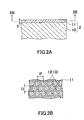
- Figs. 2(A) and 2 (B) show another embodiment of the first composite metallic material according to the present invention.
- this composite metallic material 2 a substance having conducting property higher than that of oxides of the metallic material substrate 10 (hereinafter referred to as "high conductive material”) is filled in the fine pores 12.
- the high conductive material functions as an etching core, as will be detailed later.
- the high polymer thin film 11 having a fine pore structure as the fine pattern is formed via, for example, the following steps.
- the organic solvent draws latent heat during the evaporation to thereby condense the water molecules in the air on the surface of the polymer solution into fine particles.
- the surface tension between the water and the hydrophobic organic solvent decreases.
- water fine particles agglutinate into a single mass as a fine water drop. Since the size of the water drop is approximately even, the water drops will be arranged in a closely arranged manner as the solvent evaporates, resulting in a regularly arranged state. As the water drops further evaporate, the portions where water drops existed become pores, whereby pores 12 extending in the thickness direction of the film are formed.
- the water drops function as casting molds, which forms a high polymer thin layer 11 with a honeycomb structure having a regular fine pore structure.
- Figs. 1 (B) and 2 (B) exemplify a high polymer thin film 11 in which a number of hexagonal fine pores 12 are formed in a closely arranged manner.
- the pore is often formed into a shape closed to a hexagonal shape or a circular shape other than the illustrated hexagonal shape.
- the regular fine pore structure does not mean a strict geometric regular structure but means a structure with regularity other than a random structure.
- pores having slight irregularity in pore shape, pore diameter and pore intervals fall within the meaning of the regular fine pore structure because the below-mentioned etching pits uniformly formed with high density can be formed without causing problem even if they have slight irregularity.
- the aforementioned high polymer thin film 11 can be formed on the metallic material substrate 10 in a closely adhered manner by directly casting polymer solution on the surface of the metallic material substrate. That is, the forming of the high polymer thin film 11 and the lamination of the film on the metallic material substrate 10 can be performed simultaneously. Furthermore, a high polymer thin film 11 formed on another substrate may be removed and adhered on the metallic material substrate 10.
- the substrate may be solid or liquid other than metal.
- the solid includes, for example, an inorganic material such as glass, silicon wafer and organic high polymer material excellent in organic solvent-proof such as polypropylene, polyethylen or ketone polyether.
- the liquid includes, for example, water, liquid paraffin and liquid polyether.
- water is preferably used because water is excellent in removing the high polymer thin film and holding the fine pore structure.
- the high polymer composite forming the high polymer thin film is not limited to a specific one.
- An amphiphilic high polymer compound with hydrophobic property and hydrophilic property can be exemplified as a preferable high polymer compound. It may be a homopolymer of one kind of amphiphilic molecule or a copolymer of two kinds of amphiphilic molecules. Furthermore, it may be a copolymer with molecules other than an amphiphilic molecule or may include a surfactant.
- amphiphilic high polymer compound As the aforementioned amphiphilic high polymer compound, it is preferable to use an amphiphilic high polymer compound having an ion complex of polystyrene sulfonic acid and long chain dialkyl ammonium salt, polyethylene glycol / polypropylene glycol block copolymer and acrylamide polymer as a principal chain frame, a dodecyl group as hydrophobic side chain and lactose group or carboxyl group as hydrophilic side chain, or ion complex of anion nature high polymers, such as heparin or dextran sulfuric acid, nucleic acid (DNA and RNA) and long chain alkyl ammonium salt, water-soluble protein, such as gelatin, collagen or albumin as hydrophilic group.
- anion nature high polymers such as heparin or dextran sulfuric acid, nucleic acid (DNA and RNA) and long chain alkyl ammonium salt, water-soluble protein, such as gelatin, collagen or albumin
- polystyrene phosphinic acid polystyrene sulfonic acid
- polylactic acid polycarbonate, etc.
- polycarbonate etc.
- halogen series solvent such as chloroform
- ester series such as ethyl acetate, nonaqueous ketone, carbon disulfide, etc.
- these mixed solvents can also be used.
- the density of the high polymer compound is 0.01 to 10 mass%. If the density is less than 0.01 mass%, the strength of the high polymer thin film 11 becomes insufficient. To the contrary, if it exceeds 10 mass%, it becomes difficult to form the fine pores 12 and keep the stable configuration thereof.
- the preferable density is 0.05 to 5 mass%.
- the preferable film forming environment is a high humidity atmosphere to attain the evaporation of the organic solvent and the condensation of fine water drops and the evaporation.
- the film forming is preferable performed in an atmosphere in which the relative humidity is 50 to 95% and the temperature is 10 to 25 °C.
- the preferable diameter D of the fine pore 12 is 0.01 to 50 ⁇ m. This dimension is preferably employed in a case where the composite metallic material 1 is used as an aluminum material for electrolytic capacitor electrodes to be subjected to etching processing to effectively increasing the expansion ratio by evenly forming a number of etching pits.
- the more preferable diameter D of the pore 12 is 0.1 to 5 ⁇ m.
- the pitch P of the pores is 1 to 50 ⁇ m. If it is less than 1 ⁇ m, adjacent pits may be joined at the time of etching. To the contrary, if it exceeds 50 ⁇ m, it becomes difficult to increase the number of pits. It is more preferable that the pitch of the pores 12 is 1 to 15 ⁇ m.
- the high polymer thin film 11 is preferably formed to have a thickness T of 100nm to 2 ⁇ m.
- the composite metallic material is used as an aluminum material for electrolytic capacitor electrodes, it is preferable to form the thin film to have a thickness of 0.5 to 1 ⁇ m.
- the kind of metal, the thickness, etc. are not specifically limited, and may be appropriately selected depending on the usage.
- valve-action metal used as an electrode material for electrolytic capacitor
- a metal simple substance such as aluminum, tantalum, magnesium, titanium, niobium, zirconium, zinc, bismuth or silicon, hafnium, or an alloy in which boron and tin, chromium and vanadium, or palladium and antimony are added to titanium
- an aluminum can be recommended.
- impurities may be included, or trace elements may be added if needed.
- the thickness is not limited, for the purpose of obtaining the strength and/or the flexibility after etching processing, it is preferable that the thickness is 0.05 to 0.3 mm, more preferably 0.07 to 0.2mm, the most preferably 0.07 to 0.15mm.
- the heat treatment and the crystal structure are not limited.
- a hard material to which no heat treatment is executed is formed into an aggregation of elongated fiber-like crystals elongated in the rolling direction. If such a hard material is annealed at 300 to 400°C, it becomes a soft material in which the primary recrystallization has been nearly completed, and if such a hard material is annealed at 450 to 600°C, it becomes a soft material in which crystal grains having stable high (100) sides have grown.
- either metallic material substrate mentioned above can be used.
- the metallic material substrate 10 can be a coiled elongated member or a cut member.
- the high conductive material 13 filled in the fine pores 12 is dissolved preferentially at the time of etching to become a pit-generation core, the high conductive material 13 should be selected in relation to the conductivity of the metallic material substrate 10.
- the metallic material substrate 10 is aluminum
- Pb, PbO, Cu, CuO, Cu 2 O and C whose conductivity is higher than that of aluminum can be exemplified.
- Pb and PbO can be recommended.
- plating, spattering, depositing, immersing, CVD, spray coating, ion plating, etc. can be exemplified.
- plating, depositing and immersing can be recommended because the filling speed is fast and the filling can be performed with less damage at low cost.
- the aforementioned first composite metallic material 1 and 2 is subjected to etching processing to thereby form the first etched metallic material.
- the etching liquid arrives at the metallic material via the pores 12 forming a fine pattern to thereby form etching pits. Since the etching pits 12 are arranged finely, the tunnel-like etching pits will grow in the thickness direction in accordance with the fine pattern. Thus, the fine and high density etching pits will be formed evenly, thereby enlarging the surface area. Furthermore, since the distance between the adjacent pores are kept larger than the chemical film which will be formed later, joining of pores will hardly occur. By using an etched metallic material having such etching pits such as an etched aluminum material, high capacitance can be obtained due to the enlarged surface area.
- the high conductive material 13 dissolves first and therefore the pores 12 will be exposed. Subsequently, etching pits will be formed at the portions of the metallic substrate corresponding to the pores 12. Since the high conductive materials 13 exit at the pore existing portions, in the same manner as in the composite metallic material 1, tunnel-like etching pits will be formed in accordance with the fine pattern, thereby enlarging the surface area, which in turn results in high capacitance.
- Etching processing conditions are not limited, and may be conventional conditions in accordance with the intended purpose.
- electrolytic etching is performed in the solution in which phosphoric acid, sulfuric acid, nitric acid, etc. are added in aqueous solution including chlorine ion.
- alternating current etching is generally employed in cases of material for low voltage.
- direct current etching is generally employed in cases of material for middle or high voltage.
- etching conditions alternating current etching or direct current etching of frequency of 1 to 1,000Hz, current density of 0.025 to 20 A/cm 2 , electric charge of 0.02 to 100 C/cm 2 can be exemplified.
- Direct current etching and alternating current etching can be combined. Alternatively, only direct current etching can be performed.
- multistage etching can be employed, or chemical etching can be employed.
- the aluminum material for electrolytic capacitor electrodes manufactured by the present invention can be preferably used as material for middle or high voltage, but not limited it.
- the high polymer thin film can be removed after forming the etching pits, or can be kept without removing. Furthermore, at the early etching pit forming stage, the high polymer thin film can be removed and thereafter etching processing for increasing the surface expansion ratio can be performed. In any case, the high polymer thin film can be easily removed with organic solvent such as acetone, methyl ethyl ketone, toluene, methyl cellosolve, ethyl acetate, petroleum ether, etc. Alternatively, the high polymer thin film can be easily removed by immersing into warm water whose temperature is more than the melting temperature of the high-polymer thin film.
- the etched metallic material according to the present invention include both an etched metallic material from which the high polymer thin film is removed and an etched metallic material in which the high polymer thin film remains.
- the appropriate pit of the etching pits of the etched metallic material differs depending on the working voltage of the electrolytic condenser. In cases of the material to be used at middle voltage (250 to 350 volt), it is preferable that the pit diameter is 0.7 to 2 ⁇ m and the pit distance is 1 to 2.5 ⁇ m. In cases of the material to be used at high voltage (500 volt), it is preferable that the pit diameter is 1.5 to 3 ⁇ m and the pit distance is 2 to 4 ⁇ m.
- the pit diameter mentioned above means the mean value, and it is not always required that all of the pits fall within the above range.
- electrolytic solution includes at least one of oxalic acid, adipic acid, boric acid, phosphoric acid, sodium silicate; the electrolytic solution density is 0.05 to 20 mass%; the electrolytic solution temperature is 0 to 90 °C; the current density is 0.1 mA/cm 2 to 1 A/cm 2 ; and the processing is performed for 60 minutes or less at a predetermined voltage.
- the electrolytic solution density is 0.1 to 15 mass%
- the electrolytic solution liquid temperature is 20 to 70°C
- the current density is 1 to 100 mA/cm 2
- the processing time is 30 minutes or less.
- the electrolytic capacitor by using the aforementioned etched metallic material, i.e., the metallic material with an enlarged surface area, as an electrode material, high capacitance can be obtained.
- Figs. 3 (A) and 3 (B) are schematic views showing an embodiment of the second composite metallic material according to the present invention.
- this composite metallic material 3 arranged on at least one surface of the metallic material substrate 10 are a number of fine spots 14 made of a substance with conductivity higher than that of the oxide of this metallic material substrate 10, i.e., the substance equal to the high conductive substance filled in the fine pores 12 of the aforementioned first composite metallic material 2.
- the aforementioned fine spots 14 can be formed by disposing a high polymer thin film having a number of pores on the surface of the metallic material substrate 10, filling high conductive substance whose conductivity is higher than that of the oxide of the metallic material substrate in the pores, and thereafter removing the high polymer thin film.
- the fine spots 14 can be formed by removing the high polymer thin film 11 after filling the high conductive substance 13 in the fine pores 12 of the high polymer thin film 11.
- the material and thickness of the metallic material substrate 10 and the material of the high conductive substance can be the same as in the first composite metallic material.
- the diameter D and the pitch P of the fine spots 14 of the high conductive substance can be the same as those of the pores 12 of the first composite metallic material 1 and 2.
- the step for filling the high conductive substance in the pores of the high polymer thin film 11 disposed on the surface of the metallic material substrate 10 and the steps preceding the filling step are the same as the manufacturing steps of the first composite metallic material 2. Accordingly, the method for forming the high polymer thin film 11 and the method for filling the high conductive material can be the same as those of the method for manufacturing the first composite metallic material 2.
- a dissolution removing method in which the thin film is removed by using organic solvent such as acetone, methyl ethyl ketone, toluene, methyl cellosolve, ethyl acetate, and petroleum ether and a dissolution removing method in which the thin film is removed by immersing it into warm water of a temperature higher than the melting temperature of the high polymer thin film can be exemplified.
- the aforementioned second composite metallic material 3 is subjected to etching processing, and thus the etched second metallic material according to the present invention is manufactured.
- the tunnel-like etching pits will grow in the thickness direction in accordance with the fine spots.
- the fine and high density etching pits will be formed evenly, thereby enlarging the surface area.
- joining of pores will hardly occur.
- the etching conditions can be the same as those of the manufacturing method of the aforementioned first etched metallic material.
- the appropriate pits or the chemical conversion conditions in cases of being used as an aluminum material for electrolytic capacitor electrodes can be the same as those of the etched first metallic material.
- the metallic material substrate In manufacturing the metallic material substrate, first, high purity aluminum ingots of 99.99% of Al purity were formed in accordance with semi-continuous casting. Then, these ingots were subjected to homogenization processing, surface cutting, hot rolling, cold rolling, process annealing, etc. by conventional methods and rolled into foils. Thus, aluminum material substrates 10 of 110 ⁇ m thickness were manufactured. These aluminum material substrates 10 were subjected to degreasing washing, and then disposed in an annealing furnace of Ar gas atmosphere. In the furnace, the actual temperature was raised from room temperature to 540 °C at the rate of 50 °C/h and then the substrates were kept for 24 hours at 540°C. Thereafter, the substrates were cooled naturally in the furnace. These substrates were used as common aluminum material substrates in the following examples.
- Plural kinds of composite aluminum materials I-A, I-B, I-C, I-D were formed by forming different high polymer thin films 11 of pore structure from the aluminum material substrates 10 by changing processing conditions. These composite aluminum materials I-A, I-B, I-C, I-D correspond to the first composite metallic materials 1 shown in Figs. 1 (A) and 1 (B) according to the present invention.
- a high polymer thin film 11 As polymer solution, 3 g/l chloroform solution of poly ion complex formed from polystyrene sulfonic acid and chlorination dimethyl octa decyl ammonium was prepared. Then, the polymer solution was cast to the one surface side of the aluminum material substrate 10 at the rate of 5 ml/m 2 , and high humidity air of 20 °C and 70% relative humidity were sprayed for 1 minute at the flowrate of 3 1/minute. As a result, as shown in the composite metallic material 1 shown in Fig. 1, the high polymer thin film 11 with regularly arranged hexagonal tunnel-like fine pores 12 was formed on the surface of the aluminum material substrate 10.
- the high polymer thin film 11 had the thickness T of 2 ⁇ m, and the mean diameter D of the fine pores 12 was 3 ⁇ m and the mean pore pitch P was 5 ⁇ m. Furthermore, on the other surface side of the aluminum material substrate 10, the same processing was executed to thereby form a high polymer thin film 11 with regular pore structure.
- a composite aluminum material was obtained in the same manner as in I-A except that the poly ion complex concentration was 1 g/l chloroform solution and the spraying amount of high humidity air was 2 l/minute.
- the high polymer thin film 11 had the thickness T of 2 ⁇ m, and the mean diameter D of the fine pores 12 was 2 ⁇ m and the mean pore pitch P was 3 ⁇ m.
- a composite aluminum material was obtained in the same manner as in I-A except that polycaprolactone was used instead of the polystyrene sulfonic acid of the polymer solution.
- the high polymer thin film 11 had the thickness T of 10 ⁇ m, and the mean diameter D of the fine pores 12 was 5 ⁇ m and the mean pore pitch P was 7 ⁇ m.
- a composite aluminum material was obtained in the same manner as in I-C except that the casting amount of the polymer solution was 0.5 ml/m 2 .
- the high polymer thin film 11 had the thickness T of 1 ⁇ m, and the mean diameter D of the fine pores 12 was 5 ⁇ m and the mean pore pitch P was 7 ⁇ m.
- composite aluminum material II-A, II-B, II-C and II-D having the structure of the composite metallic material 2 shown in Figs. 2 (A) and 2 (B) were formed.
- These composite aluminum material II-A, II-B, II-C and II-D correspond to the first composite metallic material of the present invention.
- Pb was filled in the fine pores of the high polymer thin film of the composite aluminum material I-A by electroplating.
- the plating were performed by passing current for 30 seconds at the current density of 1 A/m 2 by using a Pb plate as anode.
- Cu was filled in the fine pores of the high polymer thin film of the composite aluminum material I-B by electroplating.
- the plating were performed by passing current for 30 seconds at the current density of 1 A/m 2 by using a Cu plate as anode.
- the composite aluminum material I-D was immersed in the solution of Pb ion concentration of 0.5 mol/l for two minutes and then dried in a dryer at 80 °C to thereby fill Pb compound (oxide) in the pores of the high polymer thin film.
- composite aluminum material II-A, II-B and II-C was removed from each of these composite aluminum material II-A, II-B and II-C to thereby form composite aluminum material substrates III-A, III-B and III-C in which fine spots 14 of high conductive substrate were arranged on the surface of the metallic material substrate 10.
- composite aluminum material III-A, III-B and III-C correspond to the third composite metallic material 3 of the present invention shown in Figs. 3 (A) and 3 (B).
- the high polymer thin film was removed by immersing the composite aluminum material III-A in acetone for one minute to thereby obtain a composite aluminum material III-A with arranged fine spots of Pb.
- the high polymer thin film was removed by immersing the composite aluminum material II-B in methyl ketone for one minute to thereby obtain a composite aluminum material III-B with arranged fine spots of Cu.
- the high polymer thin film was removed by immersing the composite aluminum material II-C in warm water of 90 °C for three minutes to thereby obtain a composite aluminum material III-C with arranged fine spots of C.
- each of the aforementioned composite aluminum materials were subjected to etching processing under any one of the following conditions A and B to thereby form No.1 to 19 etched aluminum material for electrolytic capacitor electrodes shown in Table 1. Further, in Comparative Example No. 20, an aluminum material substrate 10 with no high polymer thin film 11 was subjected to etching processing.
- a composite aluminum material was immersed in the first electrolyte of 80 °C (1 mol/l hydrochloric acid + 3.2 mol/l sulfuric acid aqueous solution) and DC of current density 0.2 A/cm 2 was applied for 100 seconds for electrolytic etching. Furthermore, the composite material was immersed in the second electrolyte of 90 °C (1.5 mol/l hydrochloric acid + 0.0056 mol/l oxalic acid aqueous solution) for 10 minutes for chemical etching.
- a composite aluminum material was immersed in 10% ferric chloride aqueous solution of 50 °C for 10 minutes. Then it was raised therefrom and washed with water. Thus, only the fine spot portions of the high polymer thin film or the fine spot portions of the high conductive substance was chemically etched. Further, it was immersed in the second electrolyte (5% hydrochloric acid +10% sulfuric acid aqueous solution) of 75 °C, and DC of current density 0.2 A/cm 2 was applied for 100 seconds for electrolytic etching. Subsequently, in the solution, chemical etching was executed for ten minutes.
- a composite metallic material according to the present invention is capable of generating high density etching pits evenly based on the fine pattern regularly arranged in the high polymer thin film. Deep tunnel-like etching can be performed from the pits as starting points without causing a joining of the tunnel-like etching, increasing the surface expansion ratio assuredly, which in turn can increase the capacitance of an electrolytic capacitor. As a result, an electrolytic capacitor can be decreased in size and enhanced in performance, and therefore electronics devices using the electrolytic capacitors can be decreased in size and enhanced in performance.
Landscapes
- Engineering & Computer Science (AREA)
- Power Engineering (AREA)
- Microelectronics & Electronic Packaging (AREA)
- ing And Chemical Polishing (AREA)
Abstract
A composite metallic material 1 according to the invention
is used for, e.g., electrolytic capacitors, and includes a metallic
material substrate 10 and a high polymer thin layer 11 having a
fine pattern 12 formed on at least one surface of the substrate
10 by self-organization. This high polymer thin film 11 is formed
by, for example, drying hydrophobic organic solvent solution of
high polymer compound. By subjecting this composite metallic
material 1 to etching processing, etching pits are formed uniformly
with high density based on the fine pattern.

Description
Priority is claimed to Japanese Patent Application No.
2002-17468, filed on January 25, 2002 and U.S. Provisional Patent
Application No. 60/358,372, filed on February 22, 2002, the
disclosure of which are incorporated by reference in their
entireties.
The present invention relates to a composite metallic material
having a metallic material substrate and a polymer thin film formed
on the surface of the substrate, a method for manufacturing the
composite metallic material, an etched metallic material obtained
by forming etching pits in the composite metallic material, a method
for manufacturing the etched metallic material, and an electrolytic
capacitor.
In this specification, the wording of "aluminum" is used to
mean both aluminum and its alloy.
In recent years, in view of the demands of miniaturization
of electronic devices, high density mounting of printed circuit
boards and effective mounting thereof, it has been remarkably
developed to manufacture chip- shaped miniaturized electronic parts.
In view of this, demands of increasing capacitance of electrolytic
capacitor have been increased.
Generally, an aluminum foil to be used for electrolytic
capacitors is subjected to etching processing to increase the
electric capacitance by increasing the surface expansion ratio.
Furthermore, since the surface expansion ratio increases as the
number and length of the etching pit to be formed by the etching
processing increases, various processing is performed to an
aluminum material. For example, such processing includes
controlling to (100) crystal orientation, adjusting the composition
by adding trace elements such as Cu or Pb into an aluminum material,
degreasing washing before final annealing and formation processing
of crystalline oxide film during final annealing (see, Japanese
Examined Laid-open Patent Publication No. 58-34925, Japanese
Unexamined Laid-open Patent Publication No. 3-122260, etc.).
However, simply increasing the number or the length of etching
pits has been approaching to a limit for increasing the capacitance.
In order to increase the surface expansion ratio of an aluminum
foil, it is necessary to generate etching pits uniformly with high
density on the etching surface by decreasing partial etching,
etching failure and surface melting. However, in the
aforementioned methods, it is not enough to generate etching pits
uniformly with high-density, and the method do not meet the demand
of capacitance which are being further increased.
Accordingly, in currently available aluminum foils,
distribution of pitting pits can not be controlled during etching
processing, causing joined tunnel-like pits, which in turn loses
the surface area to be enlarged. Thus, the current capacitance is
merely 50 to 65% to ideal capacitance. For the purpose of increasing
capacitance, although various attempts such as adhering foreign
substances or mechanically forming defects have been made, no
attempt has become successful.
In view of the aforementioned technical background, the
present invention aims to provide a composite metallic material
capable of: generating etching pits uniformly with high density;
etching deeply on the basis of the etching pits without hardly
causing joining of tunnel-like pits; and increasing the expansion
ratio assuredly to thereby increase capacitance. The present
inventin also aims to provide a method for manufacturing the
composite metallic material, an etched metallic material and a
method for manufacturing the etched metallic material.
In order to attain the aforementioned objects, the first
composite metallic material according to the present invention has
the following structure.
According to the first composite metallic material of the
present invention, etching pits with high density can be formed
in an uniformly distributed manner based on the fine pattern by
subjecting the material to etching processing, resulting in an
enlarged surface area.
In cases where the fine pattern is a fine pore structure with
a number of arranged pores, etching pits uniformly distributed with
high density can be formed. In cases where the pore has a diameter
of 0.01 to 50µm or the pores are formed at intervals of 1 to 50
µm, extremely high expansion ratio can be obtained.
Furthermore, in cases where a substance having conducting
property higher than that of oxides of the metallic material
substrate is filled in the pores, the substance having higher
conductive property can be a generation core of the etching pit,
causing etching pits uniformly distributed with high density.
In cases where the metallic material substrate is made of
valve-action metal, the composite metallic material can be used
as an electrode material for electrolytic capacitors. For example,
the valve-action material can be aluminum, which can be used as
an aluminum material for electrolytic capacitors.
According to the second composite metallic material of the
invention, since the fine spots made of material having conducting
property higher than that of oxides of the metallic material
substrate become etching pits generation cores when the composite
metallic material is subjected to etching processing, etching pits
uniformly distributed with high density can be formed, resulting
in an enlarged surface area.
In cases where the fine spot has a diameter of 0.01 to 50
µm or the fine spots are formed at intervals of 1 to 50µm, higher
expansion ratio can be obtained.
In cases the metallic material substrate is made of
valve-action metal, it can be used for an electrode material for
electrolytic capacitor electrodes. For example, the valve-action
material can be aluminum, and can be used as an aluminum material
for electrolytic capacitor electrodes.
According to the first method for manufacturing the composite
metallic material, the aforementioned first composite metallic
material can be preferably manufactured.
In cases where the hydrophobic organic solvent solution of
high polymer compound is directly cast on a surface of the metallic
material substrate and the organic solvent is dried, a high polymer
thin film with a number of arranged pores can be formed on the
metallic material substrate in a closely adhered manner, and
therefore the forming of the high polymer thin film and the
lamination of the film on the metallic material substrate can be
performed simultaneously. Furthermore, the composite metallic
material can also be manufactured by attaching a high polymer thin
film formed on another substrate other than the metallic material
substrate on a surface of a certain metallic foil substrate.
Furthermore, by filling a substance having conducting
property higher than that of oxides of the metallic material
substrate in the pores, etching pits generation cores can be formed.
This filling of the high conductive substance can be easily
performed by any one of methods including a plating method, a
depositing method and an immersing method.
Furthermore, in cases where the high polymer compound is an
amphiphilic property high polymer compound such as an ion complex
of polystyrene sulfonic acid and long chain dialkyl ammonium salt,
a high polymer thin film having a fine pore structure can be formed.
In cases where the density of the hydrophobic organic solvent
solution of high polymer compound is 0.01 to 10 mass%, a fine pore
structure having a stable fine pore pattern with a certain strength
can be formed.
Furthermore, by performing the forming of the high polymer
compound in an atmosphere of high temperature and high humidity,
a fine pattern and a fine pore structure can be formed assuredly.
According to the second method for manufacturing the
composite metallic material of the present invention, the
aforementioned second composite metallic material can be preferably
manufactured.
In cases where hydrophobic organic solvent solution of high
polymer compound is directly cast on a surface of the metallic
material substrate and dried, a high polymer thin film having a
number of arranged pores can be formed on the metallic material
substrate in a closely adhered manner, and therefore the forming
of the high polymer thin film and the lamination of the film on
the metallic material substrate can be performed simultaneously.
Furthermore, the composite metallic material can also be
manufactured by attaching a high polymer thin film formed on a
substrate other than the metallic material substrate on a surface
of a certain metallic foil substrate.
Furthermore, the filling of the substance having conducting
property higher than that of oxides of the metallic material
substrate into the pores can be easily performed by any one of
methods including a plating method, a depositing method and a
immersing method.
In cases where the high polymer compound is an amphiphilic
high polymer compound such as ion complex of polystyrene sulfonic
acid and long chain dialkyl ammonium salt, a high polymer thin film
having a pore structure can be formed.
Furthermore, in cases where the density of the hydrophobic
organic solvent solution of a high polymer compound is 0.01 to 10
mass%, a fine pattern and a fine pore structure having a stable
configuration with certain strength can be formed.
Furthermore, by performing the forming of the high polymer
compound in an atmosphere of high temperature and high humidity,
a fine pattern and a fine pore structure can be formed assuredly.
Furthermore, the high polymer thin film after the filling of
the high conductive material can be easily removed by melting, which
enables the forming of fine spots made of a high conductive material
based on the fine pattern on the surface of the metallic material
substrate.
In the first etched metallic material of the present invention,
etching pits are formed based on the fine pattern on the first
composite metallic material. Therefore, as mentioned above,
etching pits uniformly distributed with high density are formed,
and the surface area are enlarged sufficiently.
By using the etched metallic material for an etched aluminum
material for electrolytic capacitor electrodes, the electric
capacitance can be increased.
In the second etched metallic material according to the
present invention, etching pits are formed based on the fine spots
of the second composite metallic material. Therefore, as mentioned
above, etching pits uniformly distributed with high density are
formed, and the surface area are enlarged sufficiently.
By using the etched metallic material for an etched aluminum
material for electrolytic capacitor electrodes, the electric
capacitance can be increased.
According to one of the methods for manufacturing the
aforementioned first etched metallic material, the first composite
metallic material is subjected to etching processing without
removing the high polymer thin film to thereby form etching pits.
Therefore, an etched metallic material having etching pits
uniformly distributed with high density can be obtained.
According to the other of the methods for manufacturing the
aforementioned first etched metallic material, the first composite
metallic material is subjected to initial etching processing
without removing the high polymer thin film to thereby form etching
pits, and then removing the high polymer thin film and then subjected
to etching processing to thereby grow etching pits. Therefore, an
etched metallic material having etching pits uniformly distributed
with high density can be obtained.
In the methods for manufacturing these etched metallic
materials, in cases where the etched metallic material is an etched
aluminum material for electrolytic capacitor electrodes, an
electrode material with increased electric capacitance due to the
enlarged surface area can be obtained.
According to the method for manufacturing the second etched
metallic material according to the present invention, etching pits
are formed based on the fine spots by subjecting the second composite
metallic material to etching processing. Therefore, an etched
metallic material having etching pits uniformly distributed with
high density can be obtained.
In the method of manufacturing the etched metallic material,
in cases where the etched metallic material is an etched aluminum
material for electrolytic capacitor electrodes, an electrode
material with increased electric capacitance due to the enlarged
surface area an be obtained.
Since the electrolytic capacitor according to the present
invention is made of the aforementioned etched metallic material
as an electrode material, high capacitance can be obtained,
resulting in a small and high-performance electrolytic capacitor,
which in turn enables a miniaturized and high-performance
electronics device mounting the electrolytic capacitors.
Figs. 1 (A) and 1 (B) show schematic cross-sectional views
of an embodiment of the first composite metallic material according
to the present invention. In this composite metallic material 1,
the high polymer thin film 11 laminated on the surface of the
metallic material substrate 10 is a film formed by self-organization
of a high polymer compound, and has a fine pattern formed at the
time of forming the film. Although the high polymer thin film 11
may be laminated on at least one surface of the metallic material
substrate 10, in cases where the film is used for an aluminum
material for electrolytic capacitor electrodes, it is preferable
to laminate on both surfaces in order to enlarge the surface area
as large as possible.
The high polymer thin film 11 is formed by drying a hydrophobic
organic solvent solution of a high polymer compound (hereinafter
referred to as "polymer solution"). For example, when the polymer
solution is cast on the surface of the substrate and dried, the
high polymer compound is self-organized on the substrate to form
the film having a fine pattern.
As the fine pattern, the pore structure in which a number of
pores 12 are arranged as shown in Fig. 1 (B) can be exemplified.
In one embodiment of the first composite metallic material 1 of
this invention, the pores 12 function as introduction passages for
leading the etching liquid to the surface of the metallic material
substrate 10.
Furthermore, Figs. 2(A) and 2 (B) show another embodiment
of the first composite metallic material according to the present
invention. In this composite metallic material 2, a substance
having conducting property higher than that of oxides of the
metallic material substrate 10 (hereinafter referred to as "high
conductive material") is filled in the fine pores 12. The high
conductive material functions as an etching core, as will be
detailed later.
The high polymer thin film 11 having a fine pore structure
as the fine pattern is formed via, for example, the following steps.
In the polymer solution cast on the substrate, the organic
solvent draws latent heat during the evaporation to thereby condense
the water molecules in the air on the surface of the polymer solution
into fine particles. On the other hand, because of the function
of the hydrophilic portion of the polymer solution, the surface
tension between the water and the hydrophobic organic solvent
decreases. Thereby, water fine particles agglutinate into a single
mass as a fine water drop. Since the size of the water drop is
approximately even, the water drops will be arranged in a closely
arranged manner as the solvent evaporates, resulting in a regularly
arranged state. As the water drops further evaporate, the portions
where water drops existed become pores, whereby pores 12 extending
in the thickness direction of the film are formed. The water drops
function as casting molds, which forms a high polymer thin layer
11 with a honeycomb structure having a regular fine pore structure.
Figs. 1 (B) and 2 (B) exemplify a high polymer thin film 11 in which
a number of hexagonal fine pores 12 are formed in a closely arranged
manner. The pore is often formed into a shape closed to a hexagonal
shape or a circular shape other than the illustrated hexagonal shape.
Furthermore, the regular fine pore structure does not mean a strict
geometric regular structure but means a structure with regularity
other than a random structure. Accordingly, pores having slight
irregularity in pore shape, pore diameter and pore intervals fall
within the meaning of the regular fine pore structure because the
below-mentioned etching pits uniformly formed with high density
can be formed without causing problem even if they have slight
irregularity.
In manufacturing the first composite metallic material 1 and
2 of the present invention, the aforementioned high polymer thin
film 11 can be formed on the metallic material substrate 10 in a
closely adhered manner by directly casting polymer solution on the
surface of the metallic material substrate. That is, the forming
of the high polymer thin film 11 and the lamination of the film
on the metallic material substrate 10 can be performed
simultaneously. Furthermore, a high polymer thin film 11 formed
on another substrate may be removed and adhered on the metallic
material substrate 10. In cases where the high polymer thin film
is formed on another substrate, the substrate may be solid or liquid
other than metal. The solid includes, for example, an inorganic
material such as glass, silicon wafer and organic high polymer
material excellent in organic solvent-proof such as polypropylene,
polyethylen or ketone polyether. The liquid includes, for example,
water, liquid paraffin and liquid polyether. Among another
substrates, water is preferably used because water is excellent
in removing the high polymer thin film and holding the fine pore
structure.
The high polymer composite forming the high polymer thin film
is not limited to a specific one. An amphiphilic high polymer
compound with hydrophobic property and hydrophilic property can
be exemplified as a preferable high polymer compound. It may be
a homopolymer of one kind of amphiphilic molecule or a copolymer
of two kinds of amphiphilic molecules. Furthermore, it may be a
copolymer with molecules other than an amphiphilic molecule or may
include a surfactant.
As the aforementioned amphiphilic high polymer compound, it
is preferable to use an amphiphilic high polymer compound having
an ion complex of polystyrene sulfonic acid and long chain dialkyl
ammonium salt, polyethylene glycol / polypropylene glycol block
copolymer and acrylamide polymer as a principal chain frame, a
dodecyl group as hydrophobic side chain and lactose group or
carboxyl group as hydrophilic side chain, or ion complex of anion
nature high polymers, such as heparin or dextran sulfuric acid,
nucleic acid (DNA and RNA) and long chain alkyl ammonium salt,
water-soluble protein, such as gelatin, collagen or albumin as
hydrophilic group.
Furthermore, polystyrene phosphinic acid, polystyrene
sulfonic acid, polylactic acid, polycarbonate, etc. can be
exemplified as another high polymer compounds.
As a hydrophobic organic solvent for melting a high polymer
compound, halogen series solvent such as chloroform, ester series
such as ethyl acetate, nonaqueous ketone, carbon disulfide, etc.
can be exemplified, and these mixed solvents can also be used.
In the polymer solution, it is preferable that the density
of the high polymer compound is 0.01 to 10 mass%. If the density
is less than 0.01 mass%, the strength of the high polymer thin film
11 becomes insufficient. To the contrary, if it exceeds 10 mass%,
it becomes difficult to form the fine pores 12 and keep the stable
configuration thereof. The preferable density is 0.05 to 5 mass%.
The preferable film forming environment is a high humidity
atmosphere to attain the evaporation of the organic solvent and
the condensation of fine water drops and the evaporation.
Concretely, the film forming is preferable performed in an
atmosphere in which the relative humidity is 50 to 95% and the
temperature is 10 to 25 °C.
The preferable diameter D of the fine pore 12 is 0.01 to 50
µm. This dimension is preferably employed in a case where the
composite metallic material 1 is used as an aluminum material for
electrolytic capacitor electrodes to be subjected to etching
processing to effectively increasing the expansion ratio by evenly
forming a number of etching pits. The more preferable diameter D
of the pore 12 is 0.1 to 5 µm.
It is preferable that the pitch P of the pores is 1 to 50
µm. If it is less than 1 µm, adjacent pits may be joined at the
time of etching. To the contrary, if it exceeds 50µm, it becomes
difficult to increase the number of pits. It is more preferable
that the pitch of the pores 12 is 1 to 15µm.
Furthermore, the high polymer thin film 11 is preferably
formed to have a thickness T of 100nm to 2µm. In cases where the
composite metallic material is used as an aluminum material for
electrolytic capacitor electrodes, it is preferable to form the
thin film to have a thickness of 0.5 to 1µm.
Regarding the metallic material substrate 10 constituting the
composite metallic material 1 and 2, the kind of metal, the thickness,
etc. are not specifically limited, and may be appropriately selected
depending on the usage.
As for the kind of metal, a valve-action metal used as an
electrode material for electrolytic capacitor can be exemplified.
As the valve-action metal, a metal simple substance such as aluminum,
tantalum, magnesium, titanium, niobium, zirconium, zinc, bismuth
or silicon, hafnium, or an alloy in which boron and tin, chromium
and vanadium, or palladium and antimony are added to titanium can
be exemplified. Among these metals, an aluminum can be recommended.
Furthermore, in these metallic material substrate, impurities may
be included, or trace elements may be added if needed. For example,
in case of aluminum, as the trace elements, Si, Fe, Cu, Pb, Zn,
Ga, Zr or the like can be exemplified. However, in the case of an
aluminum material for electrolytic capacitor electrodes, for the
purpose of restrain the generation of film defects during the
conversion treatment, it is preferable to use a high purity aluminum
of the purity of 99.9% or more.
In the case of an etched metallic material, although the
thickness is not limited, for the purpose of obtaining the strength
and/or the flexibility after etching processing, it is preferable
that the thickness is 0.05 to 0.3 mm, more preferably 0.07 to 0.2mm,
the most preferably 0.07 to 0.15mm.
Furthermore, in the metallic material substrate 10, the heat
treatment and the crystal structure are not limited. For example,
in an aluminum material, a hard material to which no heat treatment
is executed is formed into an aggregation of elongated fiber-like
crystals elongated in the rolling direction. If such a hard
material is annealed at 300 to 400°C, it becomes a soft material
in which the primary recrystallization has been nearly completed,
and if such a hard material is annealed at 450 to 600°C, it becomes
a soft material in which crystal grains having stable high (100)
sides have grown. In the present invention, either metallic
material substrate mentioned above can be used. Furthermore, the
metallic material substrate 10 can be a coiled elongated member
or a cut member.
Furthermore, since the high conductive material 13 filled in
the fine pores 12 is dissolved preferentially at the time of etching
to become a pit-generation core, the high conductive material 13
should be selected in relation to the conductivity of the metallic
material substrate 10. In the case in which the metallic material
substrate 10 is aluminum, Pb, PbO, Cu, CuO, Cu2O and C whose
conductivity is higher than that of aluminum can be exemplified.
Among these, Pb and PbO can be recommended.
As for the method for filling the high conductive material
13 into the fine pores 12, plating, spattering, depositing,
immersing, CVD, spray coating, ion plating, etc. can be exemplified.
Among these, plating, depositing and immersing can be recommended
because the filling speed is fast and the filling can be performed
with less damage at low cost.
The aforementioned first composite metallic material 1 and
2 is subjected to etching processing to thereby form the first etched
metallic material.
In the etching processing, as for the composite metallic
material 1 with the high polymer thin film 11 as shown in Figs.
1 (A) and 1 (B), the etching liquid arrives at the metallic material
via the pores 12 forming a fine pattern to thereby form etching
pits. Since the etching pits 12 are arranged finely, the
tunnel-like etching pits will grow in the thickness direction in
accordance with the fine pattern. Thus, the fine and high density
etching pits will be formed evenly, thereby enlarging the surface
area. Furthermore, since the distance between the adjacent pores
are kept larger than the chemical film which will be formed later,
joining of pores will hardly occur. By using an etched metallic
material having such etching pits such as an etched aluminum
material, high capacitance can be obtained due to the enlarged
surface area.
Furthermore, in the composite metallic material 2 in which
high conductive material 13 is filled in the pores 12 as shown in
Figs. 2(A) and 2 (B), the high conductive material 13 dissolves
first and therefore the pores 12 will be exposed. Subsequently,
etching pits will be formed at the portions of the metallic substrate
corresponding to the pores 12. Since the high conductive materials
13 exit at the pore existing portions, in the same manner as in
the composite metallic material 1, tunnel-like etching pits will
be formed in accordance with the fine pattern, thereby enlarging
the surface area, which in turn results in high capacitance.
Etching processing conditions are not limited, and may be
conventional conditions in accordance with the intended purpose.
For example, in cases of an aluminum material for electrolytic
condenser electrodes, in general, electrolytic etching is performed
in the solution in which phosphoric acid, sulfuric acid, nitric
acid, etc. are added in aqueous solution including chlorine ion.
Furthermore, in cases of material for low voltage, alternating
current etching is generally employed. In cases of material for
middle or high voltage, direct current etching is generally employed.
As for etching conditions, alternating current etching or direct
current etching of frequency of 1 to 1,000Hz, current density of
0.025 to 20 A/cm2, electric charge of 0.02 to 100 C/cm2 can be
exemplified. Direct current etching and alternating current
etching can be combined. Alternatively, only direct current
etching can be performed. Furthermore, multistage etching can be
employed, or chemical etching can be employed.
The aluminum material for electrolytic capacitor electrodes
manufactured by the present invention can be preferably used as
material for middle or high voltage, but not limited it.
The high polymer thin film can be removed after forming the
etching pits, or can be kept without removing. Furthermore, at the
early etching pit forming stage, the high polymer thin film can
be removed and thereafter etching processing for increasing the
surface expansion ratio can be performed. In any case, the high
polymer thin film can be easily removed with organic solvent such
as acetone, methyl ethyl ketone, toluene, methyl cellosolve, ethyl
acetate, petroleum ether, etc. Alternatively, the high polymer
thin film can be easily removed by immersing into warm water whose
temperature is more than the melting temperature of the high-polymer
thin film.
The etched metallic material according to the present
invention include both an etched metallic material from which the
high polymer thin film is removed and an etched metallic material
in which the high polymer thin film remains.
The appropriate pit of the etching pits of the etched metallic
material differs depending on the working voltage of the
electrolytic condenser. In cases of the material to be used at
middle voltage (250 to 350 volt), it is preferable that the pit
diameter is 0.7 to 2µm and the pit distance is 1 to 2.5µm. In
cases of the material to be used at high voltage (500 volt), it
is preferable that the pit diameter is 1.5 to 3µm and the pit
distance is 2 to 4µm. The pit diameter mentioned above means the
mean value, and it is not always required that all of the pits fall
within the above range.
Although the etched aluminum material for electrolytic
condenser electrodes are subjected to chemical conversion, the
conditions are not limited. The conditions can be exemplified as
follows: electrolytic solution includes at least one of oxalic acid,
adipic acid, boric acid, phosphoric acid, sodium silicate; the
electrolytic solution density is 0.05 to 20 mass%; the electrolytic
solution temperature is 0 to 90 °C; the current density is 0.1 mA/cm2
to 1 A/cm2; and the processing is performed for 60 minutes or less
at a predetermined voltage. More preferably, the electrolytic
solution density is 0.1 to 15 mass%, the electrolytic solution
liquid temperature is 20 to 70°C, the current density is 1 to 100
mA/cm2, the processing time is 30 minutes or less. After the
chemical conversion processing, if necessary, phosphoric acid
immersing processing for waterproof improvement, heat treatment
or immersing processing to boiling water for coat strengthening
can be performed.
Furthermore, in the electrolytic capacitor, by using the
aforementioned etched metallic material, i.e., the metallic
material with an enlarged surface area, as an electrode material,
high capacitance can be obtained.
Figs. 3 (A) and 3 (B) are schematic views showing an embodiment
of the second composite metallic material according to the present
invention. In this composite metallic material 3, arranged on at
least one surface of the metallic material substrate 10 are a number
of fine spots 14 made of a substance with conductivity higher than
that of the oxide of this metallic material substrate 10, i.e.,
the substance equal to the high conductive substance filled in the
fine pores 12 of the aforementioned first composite metallic material
2.
The aforementioned fine spots 14 can be formed by disposing
a high polymer thin film having a number of pores on the surface
of the metallic material substrate 10, filling high conductive
substance whose conductivity is higher than that of the oxide of
the metallic material substrate in the pores, and thereafter
removing the high polymer thin film. In other words, in the first
manufacturing method of the aforementioned composite metallic
material 2, the fine spots 14 can be formed by removing the high
polymer thin film 11 after filling the high conductive substance
13 in the fine pores 12 of the high polymer thin film 11. Accordingly,
in the second composite metallic material, the material and
thickness of the metallic material substrate 10 and the material
of the high conductive substance can be the same as in the first
composite metallic material. Furthermore, the diameter D and the
pitch P of the fine spots 14 of the high conductive substance can
be the same as those of the pores 12 of the first composite metallic
material 1 and 2.
Furthermore, regarding the manufacturing method of the second
composite metallic material 3, the step for filling the high
conductive substance in the pores of the high polymer thin film
11 disposed on the surface of the metallic material substrate 10
and the steps preceding the filling step are the same as the
manufacturing steps of the first composite metallic material 2.
Accordingly, the method for forming the high polymer thin film 11
and the method for filling the high conductive material can be the
same as those of the method for manufacturing the first composite
metallic material 2.
As the method for removing the high polymer thin film 11, a
dissolution removing method in which the thin film is removed by
using organic solvent such as acetone, methyl ethyl ketone, toluene,
methyl cellosolve, ethyl acetate, and petroleum ether and a
dissolution removing method in which the thin film is removed by
immersing it into warm water of a temperature higher than the melting
temperature of the high polymer thin film can be exemplified.
The aforementioned second composite metallic material 3 is
subjected to etching processing, and thus the etched second metallic
material according to the present invention is manufactured.
In the etching processing, since the high conductive material
is arranged in the fine spots 14, the tunnel-like etching pits will
grow in the thickness direction in accordance with the fine spots.
Thus, the fine and high density etching pits will be formed evenly,
thereby enlarging the surface area. Furthermore, since the
distance between the adjacent pores are kept larger than the
chemical film which will be formed later, joining of pores will
hardly occur. By using an etched metallic material having such
etching pits such as an etched aluminum material, high capacitance
can be obtained due to the enlarged surface area.
The etching conditions can be the same as those of the
manufacturing method of the aforementioned first etched metallic
material. The appropriate pits or the chemical conversion
conditions in cases of being used as an aluminum material for
electrolytic capacitor electrodes can be the same as those of the
etched first metallic material.
In manufacturing the metallic material substrate, first, high
purity aluminum ingots of 99.99% of Al purity were formed in
accordance with semi-continuous casting. Then, these ingots were
subjected to homogenization processing, surface cutting, hot
rolling, cold rolling, process annealing, etc. by conventional
methods and rolled into foils. Thus, aluminum material substrates
10 of 110µm thickness were manufactured. These aluminum material
substrates 10 were subjected to degreasing washing, and then
disposed in an annealing furnace of Ar gas atmosphere. In the
furnace, the actual temperature was raised from room temperature
to 540 °C at the rate of 50 °C/h and then the substrates were kept
for 24 hours at 540°C. Thereafter, the substrates were cooled
naturally in the furnace. These substrates were used as common
aluminum material substrates in the following examples.
Plural kinds of composite aluminum materials I-A, I-B, I-C,
I-D were formed by forming different high polymer thin films
11 of pore structure from the aluminum material substrates 10 by
changing processing conditions. These composite aluminum
materials I-A, I-B, I-C, I-D correspond to the first composite
metallic materials 1 shown in Figs. 1 (A) and 1 (B) according to
the present invention.
In forming a high polymer thin film 11, as polymer solution,
3 g/l chloroform solution of poly ion complex formed from
polystyrene sulfonic acid and chlorination dimethyl octa decyl
ammonium was prepared. Then, the polymer solution was cast to the
one surface side of the aluminum material substrate 10 at the rate
of 5 ml/m2, and high humidity air of 20 °C and 70% relative humidity
were sprayed for 1 minute at the flowrate of 3 1/minute. As a result,
as shown in the composite metallic material 1 shown in Fig. 1, the
high polymer thin film 11 with regularly arranged hexagonal
tunnel-like fine pores 12 was formed on the surface of the aluminum
material substrate 10. The high polymer thin film 11 had the
thickness T of 2 µm, and the mean diameter D of the fine pores 12
was 3 µm and the mean pore pitch P was 5 µm. Furthermore, on the
other surface side of the aluminum material substrate 10, the same
processing was executed to thereby form a high polymer thin film
11 with regular pore structure.
A composite aluminum material was obtained in the same manner
as in I-A except that the poly ion complex concentration was 1 g/l
chloroform solution and the spraying amount of high humidity air
was 2 l/minute. The high polymer thin film 11 had the thickness
T of 2 µm, and the mean diameter D of the fine pores 12 was 2 µm
and the mean pore pitch P was 3 µm.
A composite aluminum material was obtained in the same manner
as in I-A except that polycaprolactone was used instead of the
polystyrene sulfonic acid of the polymer solution. The high
polymer thin film 11 had the thickness T of 10 µm, and the mean
diameter D of the fine pores 12 was 5 µm and the mean pore pitch
P was 7 µm.
A composite aluminum material was obtained in the same manner
as in I-C except that the casting amount of the polymer solution
was 0.5 ml/m2. The high polymer thin film 11 had the thickness T
of 1 µm, and the mean diameter D of the fine pores 12 was 5 µm
and the mean pore pitch P was 7 µm.
Furthermore, high conductive substance were filled in the
fine pores 12 of the high polymer thin film 11 of these composite
aluminum material I-A, I-B, I-C and I-D. Thus, composite aluminum
material II-A, II-B, II-C and II-D having the structure of the
composite metallic material 2 shown in Figs. 2 (A) and 2 (B) were
formed. These composite aluminum material II-A, II-B, II-C and
II-D correspond to the first composite metallic material of the
present invention.
Pb was filled in the fine pores of the high polymer thin film
of the composite aluminum material I-A by electroplating. The
plating were performed by passing current for 30 seconds at the
current density of 1 A/m2 by using a Pb plate as anode.
Cu was filled in the fine pores of the high polymer thin film
of the composite aluminum material I-B by electroplating. The
plating were performed by passing current for 30 seconds at the
current density of 1 A/m2 by using a Cu plate as anode.
C was deposited on the composite aluminum material I-C by
normal method to fill C in the fine pores of the high polymer thin
film.
The composite aluminum material I-D was immersed in the
solution of Pb ion concentration of 0.5 mol/l for two minutes and
then dried in a dryer at 80 °C to thereby fill Pb compound (oxide)
in the pores of the high polymer thin film.
Furthermore, the high polymer thin film 11 was removed from
each of these composite aluminum material II-A, II-B and II-C to
thereby form composite aluminum material substrates III-A, III-B
and III-C in which fine spots 14 of high conductive substrate were
arranged on the surface of the metallic material substrate 10.
These composite aluminum material III-A, III-B and III-C correspond
to the third composite metallic material 3 of the present invention
shown in Figs. 3 (A) and 3 (B).
The high polymer thin film was removed by immersing the
composite aluminum material III-A in acetone for one minute to
thereby obtain a composite aluminum material III-A with arranged
fine spots of Pb.
The high polymer thin film was removed by immersing the
composite aluminum material II-B in methyl ketone for one minute
to thereby obtain a composite aluminum material III-B with arranged
fine spots of Cu.
The high polymer thin film was removed by immersing the
composite aluminum material II-C in warm water of 90 °C for three
minutes to thereby obtain a composite aluminum material III-C with
arranged fine spots of C.
Next, in each Example, each of the aforementioned composite
aluminum materials were subjected to etching processing under any
one of the following conditions A and B to thereby form No.1 to
19 etched aluminum material for electrolytic capacitor electrodes
shown in Table 1. Further, in Comparative Example No. 20, an
aluminum material substrate 10 with no high polymer thin film 11
was subjected to etching processing.
A composite aluminum material was immersed in the first
electrolyte of 80 °C (1 mol/l hydrochloric acid + 3.2 mol/l sulfuric
acid aqueous solution) and DC of current density 0.2 A/cm2 was
applied for 100 seconds for electrolytic etching. Furthermore, the
composite material was immersed in the second electrolyte of 90 °C
(1.5 mol/l hydrochloric acid + 0.0056 mol/l oxalic acid aqueous
solution) for 10 minutes for chemical etching.
A composite aluminum material was immersed in 10% ferric
chloride aqueous solution of 50 °C for 10 minutes. Then it was
raised therefrom and washed with water. Thus, only the fine spot
portions of the high polymer thin film or the fine spot portions
of the high conductive substance was chemically etched. Further,
it was immersed in the second electrolyte (5% hydrochloric acid
+10% sulfuric acid aqueous solution) of 75 °C, and DC of current
density 0.2 A/cm2 was applied for 100 seconds for electrolytic
etching. Subsequently, in the solution, chemical etching was
executed for ten minutes.
Regarding the aluminum material for electrolytic capacitor
electrodes etched in the aforementioned Examples and Comparative
Example, the pit diameter of etching pit and pit interval were
measured. The measured results are shown in Table 1. It shows that
these measured values of more than one half of the pits fall within
the range.
On the other hand, etched aluminum materials for electrolytic
capacitor electrodes were subjected to chemical conversion in Boric
acid bath at 350 V, and each capacitance was measured. The
capacitance is shown in Table 1 as a relative value provided that
the capacitor of Comparative Example No. 20 is 100%.

From the results shown in Table 1, it is confirmed that the
etched aluminum materials for electrolytic capacitor electrodes
manufactured in each Example are more uniform in etching pit
diameter and interval as compared to Comparative Example and can
obtain high capacitance due to the increased surface expansion ratio.
On the other hand, in Comparative Example, some etching pits are
joined, some etching pits are formed larger and the pit intervals
are uneven.
The terms and descriptions in this specification are used only
for explanatory purposes and the present invention is not limited
to these, but many modifications and substitutions may be made
without departing from the spirit of the scope of the present
invention which is defined by the appended claims.
A composite metallic material according to the present
invention is capable of generating high density etching pits evenly
based on the fine pattern regularly arranged in the high polymer
thin film. Deep tunnel-like etching can be performed from the pits
as starting points without causing a joining of the tunnel-like
etching, increasing the surface expansion ratio assuredly, which
in turn can increase the capacitance of an electrolytic capacitor.
As a result, an electrolytic capacitor can be decreased in size
and enhanced in performance, and therefore electronics devices
using the electrolytic capacitors can be decreased in size and
enhanced in performance.
Claims (44)
- A composite metallic material, comprising:a metallic material substrate; anda high polymer thin layer having a fine pattern formed on at least one surface of the substrate by self-organization.
- The composite metallic material as recited in claim 1, wherein the high polymer thin film is a film formed by drying hydrophobic organic solvent solution of a high polymer compound.
- The composite metallic material as recited in claim 1 or 2, wherein the fine pattern is a fine pore structure with a number of arranged pores.
- The composite metallic material as recited in claim 3, wherein the pore has a diameter of 0.01 to 50µm.
- The composite metallic material as recited in claim 3 or 4, wherein the pores are formed at intervals of 1 to 50 µm.
- The composite metallic material as recited in any one of claims 3 to 5, wherein a substance having conducting property higher than that of oxides of the metallic material substrate is filled in the pores.
- The composite metallic material as recited in any one of claims 1 to 6, wherein the metallic material substrate is made of valve-action metal.
- The composite metallic material as recited in claim 7, wherein the valve-action metal is aluminum.
- The composite metallic material as recited in claim 8, wherein the composite metallic material is an aluminum material for electrolytic capacitor electrodes.
- A composite metallic material, comprising:a metallic material substrate; anda number of fine spots made of material having conducting property higher than that of oxides of the metallic material substrate, the fine spots being arranged on at least one surface of the metallic material substrate.
- The composite metallic material as recited in claim 10, wherein the fine spot has a diameter of 0.01 to 50 µm.
- The composite metallic material as recited in claim 11 or 12, wherein the fine spots are formed at intervals of 1 to 50 µm.
- The composite metallic material as recited in any one of claims 10 to 12, wherein the metallic material substrate is made of valve-action metal.
- The composite metallic material as recited in claim 13, wherein the valve-action metal is aluminum.
- The composite metallic material as recited in claim 14, wherein the composite metallic material is an aluminum material for electrolytic capacitor electrodes.
- A method for manufacturing a composite metallic material comprising a metallic material substrate and a high polymer thin layer having a fine pattern formed on at least one surface of the substrate by self-organization, wherein the high polymer thin film is formed by drying hydrophobic organic solvent solution of a high polymer compound.
- The method for manufacturing the composite metallic material as recited in claim 16, comprising:casting hydrophobic organic solvent solution of a high polymer compound on a surface of the metallic material substrate;evaporating the organic solvent to make dew on a surface of the solution; andevaporating minute water drops generated by the dew to thereby form a high polymer thin film having a number of arranged pores.
- The method for manufacturing the composite metallic material as recited in claim 16, comprising:casting hydrophobic organic solvent solution of a high polymer compound on a surface of another substrate other than the metallic material substrate;evaporating the organic solvent to make dew on a surface of the solution;evaporating minute water drops generated by the dew to thereby form a high polymer thin film having a number of arranged pores;removing the high polymer thin film from the another substrate; andattaching the removed high polymer thin film on a surface of the metallic material substrate.
- The method for manufacturing the composite metallic material as recited in claim 17 or 18, further comprising the step of filling a substance having conducting property higher than that of oxides of the metallic material substrate in the pores.
- The method for manufacturing the composite metallic material as recited in claim 19, wherein the step of filling the substance having conducting property higher than that of oxides of the metallic material substrate is performed by any one of methods consisting of a plating method, a depositing method and an immersing method.
- The method for manufacturing the composite metallic material as recited in any one of claims 16 to 20, wherein the high polymer compound is amphiphilic high polymer compound.
- The method for manufacturing the composite metallic material as recited in claim 21, wherein the amphiphilic high polymer compound is ion complex of polystyrene sulfonic acid and long chain dialkyl ammonium salt.
- The method for manufacturing the composite metallic material as recited in any one of claims 16 to 22, wherein the density of the hydrophobic organic solvent solution of high polymer compound is 0.01 to 10 mass%.
- The method for manufacturing the composite metallic material as recited in any one of claims 16 to 23, wherein the forming of the high polymer thin layer is performed in an atmosphere of high temperature and high humidity.
- A method for manufacturing a composite metallic material comprising a metallic material substrate and a number of fine spots made of material having conducting property higher than that of oxides of the metallic material substrate, the fine spots being arranged on at least one surface of the metallic material substrate, the method, comprising:disposing a high polymer thin film having a number of arranged pores on a surface of the metallic material substrate;filling a substance having conducting property higher than that of oxides of the metallic material substrate in the pores; and thereafter;removing the high polymer thin film.
- The method for manufacturing a composite metallic material as recited in claim 25, comprising:casting hydrophobic organic solvent solution of high polymer compound on a surface of the metallic material substrate;evaporating the organic solvent to make dew on a surface of the solution; andevaporating minute water drops generated by the dew to thereby form a high polymer thin film and dispose the high polymer thin film on the metallic material substrate.
- The method for manufacturing a composite metallic material as recited in claim 25, comprising:casting hydrophobic organic solvent solution of high polymer compound on a surface of another substrate other than the metallic material substrate;evaporating the organic solvent to make dew on a surface of the solution;evaporating minute water drops generated by the dew to thereby form a high polymer thin film having a number of arranged pores;removing the high polymer thin film from the another substrate; andattaching the removed high polymer thin film on a surface of the metallic material substrate to dispose it thereon.
- The method for manufacturing the composite metallic material as recited in any one of claims 25 to 27, wherein the step of filling the substance having conducting property higher than that of oxides of the metallic material substrate is performed by any one of methods consisting of a plating method, a depositing method and an immersing method.
- The method for manufacturing the composite metallic material as recited in any one of claims 25 to 28, wherein the high polymer compound is an amphiphilic high polymer compound.
- The method for manufacturing the composite metallic material as recited in claim 29, wherein the amphiphilic high polymer compound is ion complex of polystyrene sulfonic acid and long chain dialkyl ammonium salt.
- The method for manufacturing the composite metallic material as recited in any one of claims 25 to 30, wherein the density of the hydrophobic organic solvent solution of high polymer compound is 0.01 to 10 mass%.
- The method for manufacturing the composite metallic material as recited in any one of claims 25 to 31, wherein the forming of the high polymer thin film is performed in an atmosphere of high temperature and high humidity.
- The method for manufacturing the composite metallic material as recited in any one of claims 25 to 32, wherein the removing of the high polymer thin film is performed by melting.
- An etched metallic material having etching pits formed based on the fine pattern in a composite metallic material as recited in any one of claims 1 to 9.
- The etched metallic material as recited in claim 34, wherein the etched metallic material is an etched aluminum material for electrolytic capacitor electrodes.
- An etched metallic material having etching pits formed based on the fine spots in the composite metallic material as recited in any one of claims 10 to 15.
- The etched metallic material as recited in claim 36, wherein the etched metallic material is an etched aluminum material for electrolytic capacitor electrodes.
- A method for manufacturing an etched metallic material having etching pits, wherein the etching pits are formed by subjecting a composite metallic material as recited in any one of claims 1 to 9 to etching processing without removing the high polymer thin film.
- A method for manufacturing an etched metallic material having etching pits, wherein the etching pits are formed by subjecting a composite metallic material as recited in any one of claims 1 to 9 to initial etching processing without removing the high polymer thin film, thereafter removing the high polymer thin film and further subjecting the composite metallic material to etching processing to grow the etching pits.
- The method for manufacturing the etched metallic material as recited in claim 38 or 39, wherein the etched metallic material is an etched aluminum material for electrolytic capacitor electrodes.
- A method for manufacturing an etched metallic material having etching pits, wherein the etching pits are formed by subjecting a composite metallic material as recited in any one of claims 10 to 15 to etching processing.
- The method for manufacturing the etched metallic material as recited in claim 41, wherein the etched metallic material is an etched aluminum material for electrolytic capacitor electrodes.
- An electrolytic capacitor made of an etched metallic material as recited in claim 34 or 35 as an electrode material.
- An electrolytic capacitor made of an etched metallic material as recited in claim 36 or 37 as an electrode material.
Applications Claiming Priority (5)
| Application Number | Priority Date | Filing Date | Title |
|---|---|---|---|
| JP2002017468 | 2002-01-25 | ||
| JP2002017468 | 2002-01-25 | ||
| US35837202P | 2002-02-22 | 2002-02-22 | |
| US358372P | 2002-02-22 | ||
| PCT/JP2003/000652 WO2003062506A1 (en) | 2002-01-25 | 2003-01-24 | Composite metal material and production method therefor, etched metal material and production method therefor, and electrolytic capacitor |
Publications (2)
| Publication Number | Publication Date |
|---|---|
| EP1477589A1 true EP1477589A1 (en) | 2004-11-17 |
| EP1477589A4 EP1477589A4 (en) | 2007-12-12 |
Family
ID=27615706
Family Applications (1)
| Application Number | Title | Priority Date | Filing Date |
|---|---|---|---|
| EP03703046A Withdrawn EP1477589A4 (en) | 2002-01-25 | 2003-01-24 | Composite metal material and production method therefor, etched metal material and production method therefor, and electrolytic capacitor |
Country Status (3)
| Country | Link |
|---|---|
| EP (1) | EP1477589A4 (en) |
| CN (1) | CN1639392A (en) |
| WO (1) | WO2003062506A1 (en) |
Families Citing this family (9)
| Publication number | Priority date | Publication date | Assignee | Title |
|---|---|---|---|---|
| JP2005294595A (en) * | 2004-03-31 | 2005-10-20 | Nippon Chemicon Corp | Electrolytic capacitor |
| JP2005294596A (en) * | 2004-03-31 | 2005-10-20 | Nippon Chemicon Corp | Electrolytic capacitor |
| WO2006022358A1 (en) * | 2004-08-24 | 2006-03-02 | Teijin Limited | Laminated body |
| US20100209692A1 (en) * | 2007-09-21 | 2010-08-19 | Fujifilm Corporation | Multilayer film and production method of the same |
| JP5279315B2 (en) * | 2008-03-31 | 2013-09-04 | 富士フイルム株式会社 | Method for producing porous film |
| JP5522048B2 (en) * | 2008-10-10 | 2014-06-18 | パナソニック株式会社 | Capacitor electrode foil, manufacturing method thereof, and solid electrolytic capacitor using the electrode foil |
| CN101967673A (en) * | 2010-08-27 | 2011-02-09 | 中国科学院海洋研究所 | Method for preparing super-hydrophobic film on aluminum metal surface by using electrolytic etching |
| US9202639B2 (en) * | 2012-08-17 | 2015-12-01 | Nokia Technologies Oy | Apparatus and associated methods |
| CN108302319B8 (en) * | 2017-07-13 | 2021-06-25 | 哈工大泰州创新科技研究院有限公司 | Speckled composite metal material |
Family Cites Families (5)
| Publication number | Priority date | Publication date | Assignee | Title |
|---|---|---|---|---|
| JPS6151818A (en) * | 1984-08-21 | 1986-03-14 | 昭和アルミニウム株式会社 | Method of producing aluminum electrode material for electrolytic condenser |
| EP0459461B1 (en) * | 1990-05-31 | 1995-08-23 | Toshiba Tungaloy Co. Ltd. | Multi-colored product and process for producing the same |
| JP3440610B2 (en) * | 1995-03-16 | 2003-08-25 | 凸版印刷株式会社 | Lead frame manufacturing method |
| JP3655157B2 (en) * | 1998-12-28 | 2005-06-02 | 株式会社東芝 | Magnetic recording apparatus, magnetic recording medium and manufacturing method thereof |
| JP3940546B2 (en) * | 1999-06-07 | 2007-07-04 | 株式会社東芝 | Pattern forming method and pattern forming material |
-
2003
- 2003-01-24 CN CN 03804541 patent/CN1639392A/en active Pending
- 2003-01-24 WO PCT/JP2003/000652 patent/WO2003062506A1/en not_active Ceased
- 2003-01-24 EP EP03703046A patent/EP1477589A4/en not_active Withdrawn
Also Published As
| Publication number | Publication date |
|---|---|
| CN1639392A (en) | 2005-07-13 |
| WO2003062506A1 (en) | 2003-07-31 |
| EP1477589A4 (en) | 2007-12-12 |
Similar Documents
| Publication | Publication Date | Title |
|---|---|---|
| EP1477589A1 (en) | Composite metal material and production method therefor, etched metal material and production method therefor, and electrolytic capacitor | |
| US6855408B2 (en) | Composite metal material and method for manufacturing the same, etched metal material and method for manufacturing the same and electrolytic capacitor | |
| EP2947671A1 (en) | Method for producing electrode material for aluminum electrolytic capacitors, and electrode material for aluminum electrolytic capacitors | |
| US20080094781A1 (en) | Electrode Sheet for Capacitors, Method of Manufacturing the Same, and Electrolytic Capacitor | |
| KR101251101B1 (en) | Porous valve metal thin film, method for production thereof and thin film capacitor | |
| JP2004524686A (en) | Electrolytic capacitor and method for producing the same | |
| KR100861959B1 (en) | Method for oxide dielectric layer formation, and capacitor layer forming material comprising oxide dielectric layer formed by said formation method | |
| JPH05294796A (en) | Metallic member provided with alumina crystalline growing layer and production therefor | |
| JPH0722094B2 (en) | Method for manufacturing aluminum material for electrolytic capacitor electrode | |
| JP3958343B2 (en) | Method for forming oxide dielectric layer and capacitor layer forming material having oxide dielectric layer obtained by the method | |
| JPH07201673A (en) | Method for manufacturing aluminum material for electrolytic capacitor electrode | |
| JPWO2003062506A1 (en) | Composite metal material and manufacturing method thereof, etched metal material and manufacturing method thereof, and electrolytic capacitor | |
| CN100380544C (en) | Aluminum foil for electrolytic capacitor electrode and manufacturing method thereof | |
| JP5053702B2 (en) | Capacitor electrode sheet and manufacturing method thereof | |
| JPH01316924A (en) | Aluminum material for electrolytic capacitor electrode and manufacture thereof | |
| JP2003193260A (en) | Aluminum foil for electrolytic capacitor electrode having excellent etching property, production method therefor, and method of producing aluminum etched foil for electrolytic capacitor electrode | |
| JP2635357B2 (en) | Manufacturing method of aluminum material for electrolytic capacitor | |
| CN114061347B (en) | Foam metal liquid absorption core, preparation method thereof and soaking plate | |
| JP2006328531A5 (en) | ||
| JP4421701B2 (en) | Aluminum foil for electrolytic capacitor electrode | |
| WO2005091318A1 (en) | Electrode sheet for capacitors, method for manufacturing the same, and electrolytic capacitor | |
| JPS63124406A (en) | Aluminum electrode foil for electrolytic capacitor with excellent etching characteristics and manufacture of the same | |
| JPH0864481A (en) | Electrode foil for electrolytic capacitor and manufacturing method thereof | |
| JPH118153A (en) | Method for producing polymer thin film and method for producing capacitor | |
| JPH0432553A (en) | Production of electrode foil for electrolytic capacitor |
Legal Events
| Date | Code | Title | Description |
|---|---|---|---|
| PUAI | Public reference made under article 153(3) epc to a published international application that has entered the european phase |
Free format text: ORIGINAL CODE: 0009012 |
|
| 17P | Request for examination filed |
Effective date: 20040813 |
|
| AK | Designated contracting states |
Kind code of ref document: A1 Designated state(s): AT BE BG CH CY CZ DE DK EE ES FI FR GB GR HU IE IT LI LU MC NL PT SE SI SK TR |
|
| AX | Request for extension of the european patent |
Extension state: AL LT LV MK RO |
|
| A4 | Supplementary search report drawn up and despatched |
Effective date: 20071109 |
|
| STAA | Information on the status of an ep patent application or granted ep patent |
Free format text: STATUS: THE APPLICATION IS DEEMED TO BE WITHDRAWN |
|
| 18D | Application deemed to be withdrawn |
Effective date: 20080208 |