EP1476878B1 - Memory cell with non-destructive one-time programming - Google Patents
Memory cell with non-destructive one-time programming Download PDFInfo
- Publication number
- EP1476878B1 EP1476878B1 EP03739527A EP03739527A EP1476878B1 EP 1476878 B1 EP1476878 B1 EP 1476878B1 EP 03739527 A EP03739527 A EP 03739527A EP 03739527 A EP03739527 A EP 03739527A EP 1476878 B1 EP1476878 B1 EP 1476878B1
- Authority
- EP
- European Patent Office
- Prior art keywords
- value
- memory
- resistance
- resistor
- programming
- Prior art date
- Legal status (The legal status is an assumption and is not a legal conclusion. Google has not performed a legal analysis and makes no representation as to the accuracy of the status listed.)
- Expired - Lifetime
Links
Images


Classifications
-
- G—PHYSICS
- G11—INFORMATION STORAGE
- G11C—STATIC STORES
- G11C17/00—Read-only memories programmable only once; Semi-permanent stores, e.g. manually-replaceable information cards
- G11C17/14—Read-only memories programmable only once; Semi-permanent stores, e.g. manually-replaceable information cards in which contents are determined by selectively establishing, breaking or modifying connecting links by permanently altering the state of coupling elements, e.g. PROM
-
- G—PHYSICS
- G11—INFORMATION STORAGE
- G11C—STATIC STORES
- G11C16/00—Erasable programmable read-only memories
- G11C16/02—Erasable programmable read-only memories electrically programmable
- G11C16/06—Auxiliary circuits, e.g. for writing into memory
- G11C16/22—Safety or protection circuits preventing unauthorised or accidental access to memory cells
Definitions
- JP-A-54 098536 discloses a memory cell comprising a transistor in series with a polycrystalline silicon resistor whose resistance is modified to program the cell.
- the reference potential is taken at the mid-point of a resistive divider bridge.
- a current for example I1 is applied across the resistive element 31, said stress, greater than a current Im for which the value of the resistance R of the element 31 is maximum without being infinite.
- this current I1 has been applied to the resistive element 31, we obtain, in the range A1 of operating currents of the integrated circuit, a stable resistance of value R1.
- the pace S name of resistance versus current is stable for relatively low currents (less than 100 ⁇ A). This pace starts to grow for currents significantly higher of the order of a few milliamperes or more (A2 range).
- the dopant concentration of the polycrystalline silicon is between 1.10 13 and 1.10 16 atoms per cubic centimeter.
- Another advantage is that the code stored in the storage element is not optically detectable unlike a silicon resistor polycrystalline used as a fuse where the physical deterioration of the silicon bar makes the programming visible.
- Another advantage is that the irreversible modification of the value of the programmed resistor is not destructive and therefore does not risk damaging other parts of the circuit. This allows in particular to provide a decrease in the value of the resistance after manufacture, and even during its life in its application circuit.
- Another advantage of the present invention is that it does not require any particular technology unlike EPROM or EEPROM type single programming memory structures.
- Another advantage of the present invention is that it is not sensitive to ultraviolet and therefore can not be erased by this means. More generally, a programmed memory cell according to the invention is indelible because of the irreversible reduction of the resistance performed.
- one or more comparators each associated with different reference divisor bridges can be added.
- a multi-level memory is then obtained, the memorized level being dependent on the value (for example, I1 or I2) of the programming current applied to the resistor Rpi of each branch.
- Several programming voltages Vp are then provided (at least functionally, for example, by means of resistive dividers).
- Each bit line BL is connected to the terminal 2 for applying a supply voltage Valim via an N channel transistor Tb1, Tb2, ..., Tbn acting as the load resistor. Rb of the previous embodiments. In practice, these are depleted transistors.
- Each bit line is connected by its other end and via a selection transistor, respectively Ts1, Ts2, ..., Tsn, to an input (for example, non-inverting) of a differential amplifier 5 readout whose output provides the status of the read cell.
- the other input (inverting) of the amplifier 5 is connected to the midpoint of a voltage divider bridge consisting of the series connection of an N-channel MOS transistor Tb 'connected to the supply voltage Vr and a resistor Rp 'connected to the reference voltage V-.
- first zone first series of resistors
- manufactured for the programming of a memory according to the invention, it will be possible to separate several distinct phases in the life of the product. For example, there is provided a first zone (first series of resistors) programmable at the end of manufacture to contain a "manufacturer" code. The rest of the memory is left available to be programmed (in one or more times) by the user (final or not).
Landscapes
- Read Only Memory (AREA)
- Semiconductor Memories (AREA)
Description
La présente invention concerne le domaine des cellules mémoire à programmation unique (OTP) et, plus particulièrement, la réalisation d'une mémoire à programmation unique en circuit intégré.The present invention relates to the field of single programming memory cells (OTP) and, more particularly, the realization of a single programming memory integrated circuit.
Classiquement, les mémoires à programmation unique en circuit intégré sont de type EPROM et requièrent donc des circuits de programmation spécifiques qui ne sont pas compatibles avec les technologies standard de fabrication des transistors MOS utilisés dans les circuits intégrés. On trouve aussi des mémoires à programmation unique réalisées par des EEPROM et des mémoires flash non effaçables.Conventionally, integrated programming memories are of the EPROM type and therefore require specific programming circuits that are not compatible with the standard technologies for manufacturing MOS transistors used in integrated circuits. There are also single programming memories made by EEPROMs and non-erasable flash memories.
Une autre catégorie de mémoires à programmation unique est constituée des mémoires fusibles ou anti-fusibles. Parmi celles-ci, on trouve des mémoires formées d'un barreau ou piste de silicium polycristallin que l'on soumet à un courant très élevé de façon à détériorer physiquement le silicium polycristallin et ouvrir le circuit. De telles cellules mémoires à programmation unique requièrent des courants très élevés (de l'ordre de la centaine de milliampères). Cela limite considérablement leur utilisation. De plus, la programmation opérée sur une cellule de type fusible est visible optiquement, ce qui nuit à la sécurité d'un code binaire enfoui dans un circuit intégré et masqué dans une mémoire à programmation unique.Another category of single programming memories consists of fusible or fuse memories. Among these are memories formed of a rod or polycrystalline silicon track that is subjected to a very high current so as to physically damage the polycrystalline silicon and open the circuit. Such single programming memory cells require very high currents (of the order of a hundred milliamperes). This greatly limits their use. In addition, the programming performed on a fuse-type cell is visible optically, which affects the security of a binary code buried in a integrated circuit and masked in a single programming memory.
Un inconvénient similaire existe avec les mémoires de type EPROM ou EEPROM, à savoir qu'une détection de l'état des cellules de mémorisation est possible au moyen d'un microscope à balayage électronique qui peut détecter la différence de charges accumulées dans les transistors à grille flottante de telles mémoires.A similar disadvantage exists with the EPROM or EEPROM type memories, namely that a detection of the state of the storage cells is possible by means of a scanning electron microscope which can detect the difference of charges accumulated in the transistors. floating gate of such memories.
La présente invention vise à proposer une nouvelle structure de cellule mémoire à programmation unique qui pallie les inconvénients des structures connues.The present invention aims to propose a new single programming memory cell structure that overcomes the disadvantages of known structures.
L'invention vise plus particulièrement à proposer la réalisation d'une cellule mémoire en circuit intégré qui ne requiert aucune étape de fabrication supplémentaire par rapport aux étapes mises en oeuvre pour la fabrication de transistors MOS dans les technologies classiques.The invention aims more particularly to propose the realization of a memory cell integrated circuit which requires no additional manufacturing step with respect to the steps implemented for the manufacture of MOS transistors in conventional technologies.
L'invention vise également à améliorer la sécurité d'un code enfoui au moyen d'une cellule mémoire à programmation unique.The invention also aims to improve the security of a code buried by means of a single programming memory cell.
L'invention vise également à proposer une cellule mémoire peu onéreuse.The invention also aims at providing an inexpensive memory cell.
L'invention vise également à proposer une mémoire à programmation unique. Le préambule de la revendication 1 est décrit par le document
Le document
Le document
Le document
Le document
Pour atteindre ces objets et d'autres, l'invention prévoit une cellule mémoire à programmation unique telle que définie par la revendication 1.To achieve these and other objects, the invention provides a single programming memory cell as defined by
Selon un mode de réalisation de la présente invention, le potentiel de référence est prélevé au point milieu d'un pont diviseur résistif.According to one embodiment of the present invention, the reference potential is taken at the mid-point of a resistive divider bridge.
Selon un mode de réalisation de la présente invention, chaque cellule présente un état non programmé qui est, par programmation, modifié en diminuant, de façon irréversible et stable dans la plage de courants de fonctionnement en lecture de la cellule, la valeur de sa résistance en silicium polycristallin.According to an embodiment of the present invention, each cell has an unprogrammed state which is, by programming, modified by irreversibly and steadily decreasing in the range of read operation currents. the cell, the value of its polycrystalline silicon resistance.
Selon un mode de réalisation de la présente invention, la programmation d'une cellule est commandée en forçant la circulation d'un courant dans sa résistance en silicium polycristallin qui soit supérieur au courant pour lequel la valeur de cette résistance présente un maximum.According to one embodiment of the present invention, the programming of a cell is controlled by forcing the flow of a current in its polycrystalline silicon resistance which is greater than the current for which the value of this resistance has a maximum.
Selon un mode de réalisation de la présente invention, plusieurs amplificateurs de lecture reçoivent des tensions de références différentes et sont tous connectés par leur première entrée à plusieurs cellules, de façon à constituer une mémoire multi-niveaux différenciés par les valeurs des résistances en silicium polycristallin.
- Ces objets, caractéristiques et avantages, ainsi que d'autres de la présente invention seront exposés en détail dans la description suivante de modes de mise en oeuvre et de réalisation particuliers, faite à titre non-limitatif en relation avec les figures jointes parmi lesquelles :
- la
figure 1 représente un premier exemple de réalisation d'une cellule mémoire à programmation unique ; - la
figure 2 représente un deuxième exemple mode de réalisation d' une cellule mémoire à programmation unique ; - la
figure 3 illustre, par une vue partielle en perspective, un mode de réalisation d'une résistance en silicium polycristallin constituant l'élément de mémorisation d'une cellule selon l'invention ; - la
figure 4 illustre, par un réseau de courbes, la programmation d'une cellule mémoire selon la présente invention ; - la
figure 5 représente un mode de réalisation d'une mémoire multicellulaire selon la présente invention ; et - la
figure 6 représente un exemple de réalisation d'une mémoire.
- la
- These and other objects, features and advantages of the present invention will be set forth in detail in the following description of particular embodiments and embodiments, given in a non-limiting manner in relation to the appended figures among which:
- the
figure 1 represents a first embodiment of a single programming memory cell; - the
figure 2 represents a second exemplary embodiment of a single programming memory cell; - the
figure 3 illustrates, in a partial perspective view, an embodiment of a polycrystalline silicon resistor constituting the storage element of a cell according to the invention; - the
figure 4 illustrates, by a network of curves, the programming of a memory cell according to the present invention; - the
figure 5 represents an embodiment of a multicell memory according to the present invention; and - the
figure 6 represents an exemplary embodiment of a memory.
- the
Les mêmes éléments ont été désignés par les mêmes références aux différentes figures. Pour des raisons de clarté, seuls les éléments qui sont nécessaires à la compréhension de l'invention ont été représentés aux figures et seront décrits par la suite. En particulier, les circuits exploitant les codes binaires au moyen de cellules selon l'invention n'ont pas été détaillés. L'invention pourra être mise en oeuvre quelle que soit l'utilisation faite du code mémorisé.The same elements have been designated by the same references in the different figures. For the sake of clarity, only those elements which are necessary for the understanding of the invention have been shown in the figures and will be described later. In particular, the circuits exploiting the binary codes by means of cells according to the invention have not been detailed. The invention may be implemented regardless of the use made of the stored code.
La
La cellule mémoire 1 comporte, en série avec une première borne 2 d'application d'un potentiel positif d'alimentation et une deuxième borne 3 d'application d'un potentiel plus négatif d'alimentation V- ou de référence (généralement la masse), une résistance programmable Rp et un interrupteur de programmation (ici, un transistor MOS à canal N MN). La résistance Rp constitue l'élément de mémorisation de la cellule 1. L'état stocké dans la cellule est lu sur le point milieu 4 de l'association en série de la résistance Rp avec le transistor MN. La lecture du niveau mémorisé s'effectue comme on le verra par la suite en relation avec la
Une caractéristique est que la résistance Rp constituant l'élément de mémorisation est une résistance en silicium polycristallin dont la valeur est programmable par diminution irréversible de sa valeur, comme cela sera exposé par la suite en relation avec les
Selon cet exemple de réalisation, pour permettre la lecture de l'état mémorisé dans la cellule 1, on prévoit une résistance Rb (représentée en pointillés en
Le transistor MN, lorsqu'il est passant, court-circuite (au moins fonctionnellement) la résistance fixe Rb et sert à programmer la résistance Rp en imposant la circulation d'un courant dans celle-ci. Le courant de programmation de la résistance Rp est supérieur au courant pour lequel cette résistance présente une valeur maximale. Cette caractéristique ressortira mieux de la description qui sera faite par la suite en relation avec les
La programmation d'une cellule telle qu'illustrée par la
La
Le fonctionnement d'une cellule 1' telle que représentée en
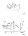
La
Une telle résistance (désignée par 31 en
La résistance R de l'élément 31 est donnée par la formule suivante : ![]()
où p désigne la résistivité du matériau (silicium polycristallin le cas échéant dopé) constituant la piste dans laquelle est gravé l'élément 31, où L désigne la longueur de l'élément 31, et où s désigne sa section, c'est-à-dire sa largeur 1 par son épaisseur e. La résistivité p de l'élément 31 dépend, entre autres, du dopage éventuel du silicium polycristallin le constituant.The resistance R of ![]()
where p denotes the resistivity of the material (optionally doped polycrystalline silicon) constituting the track in which
Le plus souvent, lors de la réalisation d'un circuit intégré, on prévoit les résistances en faisant référence à une notion dite de résistance par carreau R□ (square resistance). Cette résistance par carreau se définit comme étant la résistivité du matériau divisée par l'épaisseur avec laquelle il est déposé. En reprenant la relation ci-dessus donnant la résistance d'un élément 31, la résistance est donc donnée par la relation : ![]()
![]()
Le quotient L/1 correspond à ce que l'on appelle le nombre de carreaux (square number) constituant l'élément résistif 31. Cela représente, vu de dessus, le nombre de carreaux de dimension donnée fonction de la technologie, mis côte à côte pour former l'élément 31.The quotient L / 1 corresponds to what is called the number of squares (square number) constituting the
La valeur de la résistance en silicium polycristallin est donc définie, à la fabrication, d'après les paramètres ci-dessus, conduisant à des résistivités et résistances dites nominales. Généralement, l'épaisseur e du silicium polycristallin est fixée par d'autres paramètres de fabrication du circuit intégré. Par exemple, cette épaisseur est fixée par l'épaisseur souhaitée pour les grilles des transistors MOS du circuit intégré.The value of the polycrystalline silicon resistance is therefore defined, in the manufacture, according to the above parameters, leading to so-called nominal resistivities and resistances. Generally, the thickness e of the polycrystalline silicon is fixed by other manufacturing parameters of the integrated circuit. For example, this thickness is fixed by the desired thickness for the gates of the MOS transistors of the integrated circuit.
Une caractéristique de la présente invention est d'imposer temporairement, dans une résistance en silicium polycristallin (Rp) dont on souhaite diminuer irréversiblement la valeur, un courant de programmation ou de contrainte supérieur à un courant pour lequel la résistance passe par une valeur maximale, ce courant étant au-delà de la plage de courants de fonctionnement normal (en lecture) de cette résistance. En d'autres termes, on diminue la résistivité du silicium polycristallin dans la plage de courants de fonctionnement, de façon stable et irréversible, en imposant temporairement dans l'élément résistif correspondant la circulation d'un courant au-delà de la plage de courants de fonctionnement.A feature of the present invention is to impose temporarily, in a polycrystalline silicon resistor (Rp) which it is desired to decrease irreversibly the value, a programming current or stress greater than a current for which the resistance passes through a maximum value, this current being beyond the range of normal operating currents (read) of this resistance. In other words, the resistivity of the polycrystalline silicon in the operating current range is reduced, stably and irreversibly, by temporarily imposing in the corresponding resistive element the flow of a current beyond the current range. Operating.
Une autre caractéristique de l'invention est que le courant servant à diminuer la valeur de la résistance est, à la différence d'un élément fusible, non destructif pour l'élément en silicium polycristallin.Another feature of the invention is that the current used to reduce the value of the resistance is, unlike a fuse element, non-destructive for the polycrystalline silicon element.
La
On suppose que le silicium polycristallin ayant servi à la fabrication de l'élément résistif 31 (Rp) présente une résistivité nominale conférant à l'élément 31, pour les dimensions 1, L et e données, une valeur de résistance Rnom. Cette valeur nominale (d'origine) de la résistance correspond à la valeur prise de façon stable par l'élément résistif 31 dans la plage de courants de fonctionnement du système, c'est-à-dire généralement pour des courants inférieurs à 100 µA.It is assumed that the polycrystalline silicon used in the manufacture of the resistive element 31 (Rp) has a nominal resistivity conferring on the
Selon l'invention, pour diminuer la valeur de la résistance et passer de façon irréversible et stable, par exemple, à une valeur R1 inférieure à Rnom, on applique aux bornes de l'élément résistif 31 un courant (par exemple I1), dit de contrainte, supérieur à un courant Im pour lequel la valeur de la résistance R de l'élément 31 est maximale sans toutefois être infinie. Comme l'illustre la
En effet, une fois passé le maximum de l'allure Snom de la résistivité en fonction du courant, la valeur prise par la résistance dans la plage de courants de fonctionnement se trouve inférieure à la valeur Rnom. La nouvelle valeur, par exemple R1, dépend de la valeur la plus élevée du courant (ici, I1) qui a été appliqué pendant la phase de diminution irréversible. On notera en effet que la diminution irréversible opérée par l'invention s'effectue dans une phase spécifique de programmation, hors du fonctionnement normal en lecture (plage A1) du circuit intégré, c'est-à-dire hors du fonctionnement normal de la résistance.Indeed, once past the maximum of the Snom rate of the resistivity as a function of the current, the value taken by the resistor in the range of operating currents is lower than the value R nom . The new value, for example R1, depends on the highest value of the current (here, I1) that was applied during the irreversible decrease phase. It will be noted that the irreversible reduction effected by the invention is carried out in a specific programming phase, out of normal operation in reading (range A1) of the integrated circuit, that is to say out of the normal operation of the resistance.
Le cas échéant, une fois que la valeur de la résistance en silicium polycristallin a été abaissée vers une valeur inférieure (par exemple R1 en
On voit que toutes les allures de la résistance en fonction du courant se rejoignent sur la pente de décroissance de la valeur de la résistance, après être passé par le maximum de l'allure. Ainsi, pour un élément résistif donné (p, L, s), les courants I1, I2, etc. qui doivent être atteints, pour passer à une valeur de résistance inférieure, sont indépendants de la valeur de la résistance (Rnom, R1, R2) à partir de laquelle on provoque la diminution. En fait, le courant provoque une élévation de la température de l'élément en silicium polycristallin, ce qui entraîne son fluage.It can be seen that all the paces of the resistance as a function of the current meet on the slope of decrease of the value of the resistance, after having passed through the maximum of the pace. Thus, for a given resistive element (p, L, s), the currents I1, I2, and so on. which must be reached, to go to a lower resistance value, are independent of the value of the resistance (Rnom, R1, R2) from which the decrease is caused. In fact, the current causes an increase in the temperature of the polycrystalline silicon element, which causes its creep.
Ce qui a été exprimé ci-dessus comme valeur de résistance correspond en fait à une diminution de la résistivité du silicium polycristallin constituant l'élément résistif. Les inventeurs considèrent que l'on assiste à une modification stable de la structure cristalline du silicium polycristallin et que l'on assiste, en quelque sorte, à un fluage du matériau, la structure cristalline finale obtenue dépendant du courant maximum atteint.What has been expressed above as a resistance value corresponds in fact to a decrease in the resistivity of the polycrystalline silicon constituting the resistive element. The inventors consider that there is a stable modification of the crystalline structure of polycrystalline silicon and that we see, as it were, a creep of the material, the final crystalline structure obtained depending on the maximum current reached.
Bien sûr, on veillera à ne pas dépasser la plage de courants de programmation A2 (de l'ordre de quelques milliampères) afin de ne pas risquer de détruire la résistance en silicium polycristallin. Cette précaution ne posera en pratique pas de problème dans la mesure où l'utilisation du silicium polycristallin pour constituer un fusible requiert des courants nettement plus élevés (de l'ordre du dixième d'ampère) qui ne sont pas disponibles une fois le circuit fabriqué.Of course, care must be taken not to exceed the range of A2 programming currents (of the order of a few milliamps) in order not to risk destroying the polycrystalline silicon resistance. This precaution will not pose any problem in practice in that the use of polycrystalline silicon to constitute a fuse requires much higher currents (of the order of one-tenth of an ampere) which are not available once the circuit has been manufactured.
La réalisation pratique d'une résistance en silicium polycristallin selon l'invention ne diffère pas de la réalisation d'une résistance classique. Partant d'un substrat isolant, on dépose une couche de silicium polycristallin que l'on grave en fonction des dimensions souhaitées pour la résistance. Comme l'épaisseur de silicium polycristallin déposée est généralement fixée par la technologie, les deux dimensions que l'on peut régler sont la largeur et la longueur. Généralement, on redépose un isolant sur le barreau de silicium polycristallin ainsi obtenu. Dans le cas d'une interconnexion en ligne, on aura modifié la largeur 1 par rapport aux pistes d'accès plus larges pour être fortement conductrices. Dans le cas d'un accès aux extrémités du barreau par le dessus comme cela est illustré en
En pratique, pour disposer de la capacité de réglage de résistance la plus importante avec un courant de contrainte minimum, on cherchera à utiliser une épaisseur minimale et une largeur minimale pour les éléments résistifs. Dans ce cas, seule la longueur L conditionne la valeur nominale de la résistance une fois la structure du silicium polycristallin fixée. Le dopage éventuel du silicium polycristallin, quel que soit son type, n'entrave pas la mise en oeuvre de l'invention. La seule différence liée au dopage est la résistivité nominale avant contrainte et les résistivités obtenues pour des courants de contraintes donnés. En d'autres termes, pour un élément de dimensions données, cela conditionne le point de départ de la valeur de la résistance, et par voie de conséquence, les valeurs de résistance obtenues pour des courants de contrainte donnés.In practice, in order to have the largest resistance setting capability with a minimum stress current, the minimum thickness and minimum width for the resistive elements will be sought. In this case, only the length L conditions the nominal value of the resistor once the polycrystalline silicon structure is fixed. The possible doping of polycrystalline silicon, whatever its type, does not hinder the implementation of the invention. The only difference related to doping is the nominal resistivity before stress and the resistivities obtained for given stress currents. In other words, for an element of given dimensions, this conditions the starting point of the value of the resistance, and consequently the resistance values obtained for given stress currents.
Pour passer de la valeur nominale à une valeur de résistance ou résistivité inférieure, on peut selon l'invention utiliser plusieurs méthodes.To pass from the nominal value to a resistance value or lower resistivity, it is possible according to the invention to use several methods.
Selon un premier mode de mise en oeuvre, on fait croître progressivement (pas à pas) le courant dans la résistance. Après chaque application d'un courant supérieur, on revient dans la plage de courants de fonctionnement et on mesure la valeur de la résistance. Tant que le point Im de courant n'est pas atteint, cette valeur de résistance restera à la valeur Rnom. Dès que le point Im en courant est dépassé, on change de courbe (allure S) et la valeur mesurée lorsque l'on repasse sur les courants de fonctionnement devient une valeur inférieure à la valeur Rnom. Si cette nouvelle valeur convient, on en reste là. Dans le cas contraire, on réapplique des courants supérieurs pour dépasser la nouvelle valeur maximale de l'allure courante. Dans ce cas, il n'est pas nécessaire de repartir des courants minimaux comme lorsque l'on démarre de la résistance nominale. En effet, la valeur du courant pour laquelle la résistance va de nouveau diminuer est forcément supérieure à la valeur du courant de contrainte I1 appliqué pour passer sur l'allure courante. La détermination du pas à appliquer est à la portée de l'homme du métier et n'est pas critique en ce qu'elle conditionne essentiellement le nombre de diminutions possibles. Plus le pas est élevé, plus les sauts entre les valeurs seront importants.According to a first embodiment, the current in the resistor is gradually increased (step by step). After each application of a higher current, it returns to the range of operating currents and the value of the resistance is measured. As long as the point Im current is not reached, this resistance value will remain at the value R name . As soon as the point Im in current is exceeded, one changes curve (pace S) and the value measured when one returns to the operating currents becomes a value lower than the value R nom . If this new value is appropriate, we leave it there. In the opposite case, higher currents are reapplied to exceed the new maximum value of the current rate. In this case, it is not necessary to distribute minimum currents as when starting the nominal resistance. Indeed, the value of the current for which the resistor will decrease again is necessarily greater than the value of the constraint current I1 applied to switch to the current pace. The determination of the step to be applied is within the reach of the person skilled in the art and is not critical in that it essentially conditions the number of possible decreases. The higher the step, the more jumps between the values will be important.
Selon un deuxième mode de mise en oeuvre, on prédétermine, par exemple par mesures, les différents courants à appliquer pour passer des différentes valeurs de résistance à des valeurs inférieures. Cette prédétermination tient compte bien entendu de la nature du silicium polycristallin utilisé ainsi que préférentiellement de la résistance par carreau c'est-à-dire de la résistivité du matériau et de l'épaisseur dans laquelle il est déposé. En effet, comme les allures illustrées par la
Les deux modes de mise de oeuvre ci-dessus peuvent être combinés. On peut ainsi, dans une première étape, sélectionner une valeur approximative (dans une table) et appliquer le courant prédéterminé correspondant. Puis, dans une deuxième étape, on affine la valeur de la résistance par des diminutions pas à pas de sa valeur.The two modes of implementation above can be combined. It is thus possible, in a first step, to select an approximate value (in a table) and apply the corresponding predetermined current. Then, in a second step, the value of the resistance is refined by decreasing stepwise its value.
Selon l'invention, la diminution irréversible de la résistance ou résistivité peut être effectuée après fabrication lorsque le circuit est dans son environnement fonctionnel. En d'autres termes, le circuit 4 de commande et les transistors de programmation décrits en relation avec les
Le changement de courbes, c'est-à-dire la diminution de la valeur de résistance en fonctionnement normal est quasi immédiate dès que le courant de contrainte correspondant est appliqué. Par quasi-immédiat, on entend une durée de quelques dizaines voir centaines de microsecondes qui suffisent pour appliquer la contrainte correspondante au barreau de silicium polycristallin et diminuer la valeur de sa résistance. Cette valeur empirique dépend de la taille (physique) du barreau. On pourra choisir une durée de quelques millisecondes par sécurité. De plus, on peut considérer que, une fois la durée minimale atteinte, toute durée supplémentaire d'application du courant de contrainte ne modifie pas, au moins au premier ordre, la résistance atteinte. En outre, même si dans une application particulière on considère ne pas pouvoir négliger l'influence de la durée d'application de la contrainte, les deux modes préférés de mise en oeuvre (prédéterminer des valeurs de contraintes en durée et en intensité, ou progression pas à pas jusqu'à la valeur souhaitée) sont parfaitement compatibles avec la prise en compte de la durée d'application de la contrainte.The change of curves, that is to say the decrease of the resistance value in normal operation is almost immediate as soon as the corresponding stress current is applied. By quasi-immediate means a duration of a few tens or hundreds of microseconds sufficient to apply the corresponding stress to the polycrystalline silicon bar and reduce the value of its resistance. This empirical value depends on the (physical) size of the bar. We can choose a duration of a few milliseconds per security. Moreover, it can be considered that, once the minimum duration has been reached, any additional duration of application of the current of stress does not modify, at least in the first order, the resistance reached. Furthermore, even if in a particular application it is considered that it is not possible to neglect the influence of the duration of the application of the constraint, the two preferred modes of implementation (predetermine stress values in duration and intensity, or progression step by step until desired value) are perfectly compatible with taking into account the duration of the application of the constraint.
A titre d'exemple particulier de mise en oeuvre, on a réalisé une résistance en silicium polycristallin dopée N+ ayant une section de 0,225 micromètre carré (1 = 0,9 µm, e = 0,25 µm) et une longueur L de 45 micromètres. Avec le silicium polycristallin utilisé et le dopage correspondant, la résistance nominale était d'environ 6300 Ohms. Cela correspond à une résistance par carreau d'environ 126 Ohms (50 carreaux). En appliquant à cette résistance un courant supérieur à trois milliampères, on a provoqué une diminution de sa valeur, stable pour un fonctionnement sous des courants allant jusqu'à 500 microampères. Avec un courant de 3,1 milliampères, la valeur de la résistance a été abaissée à environ 4500 Ohms. En appliquant à la résistance un courant de 4 milliampères, on a diminué la valeur de la résistance jusqu'environ 3000 Ohms. Les valeurs obtenues de résistances ont été les mêmes pour des durées de contraintes allant de 100 microsecondes à plus de 100 secondes.As a specific example of implementation, an N + doped polycrystalline silicon resistor having a cross section of 0.225 square micrometer (1 = 0.9 μm, e = 0.25 μm) and a length L of 45 micrometers was produced. . With the polycrystalline silicon used and the corresponding doping, the nominal resistance was about 6300 ohms. This corresponds to a tile resistance of about 126 ohms (50 tiles). Applying a current greater than three milliamperes to this resistance has caused a decrease in its value, stable for operation under currents of up to 500 microamperes. With a current of 3.1 milliamps, the resistance value was lowered to about 4500 ohms. By applying a current of 4 milliamps to the resistor, the resistance value was reduced to about 3000 ohms. The values obtained from resistances were the same for durations of constraints ranging from 100 microseconds to more than 100 seconds.
Selon un exemple de mise en oeuvre particulier de l'invention, le courant de contrainte est compris entre 1 et 10 milliampères.According to an example of a particular implementation of the invention, the stress current is between 1 and 10 milliamps.
Toujours selon un exemple de mise en oeuvre particulier, la concentration en dopant du silicium polycristallin est comprise entre 1.1013 et 1.1016 atomes par centimètre cube.Still according to an example of a particular implementation, the dopant concentration of the polycrystalline silicon is between 1.10 13 and 1.10 16 atoms per cubic centimeter.
A titre d'exemple particulier, on a réalisé des résistances en silicium polycristallin ayant les caractéristiques nominales suivantes.
Bien entendu, les exemples ci-dessus ainsi que les ordres de grandeurs donnés de courants et de résistances pour les différentes plages concernent les technologies actuelles. Les courants des plages A1, A2 et A3 pourront être différents (inférieurs) pour des technologies plus avancées et peuvent être transposés à des densités de courant. Le principe de l'invention n'en est pas modifié. On a toujours trois plages et on utilise la plage intermédiaire pour forcer la diminution de résistivité.Of course, the above examples as well as the given orders of magnitude of currents and resistances for the different ranges relate to current technologies. The currents of the ranges A1, A2 and A3 may be different (lower) for more advanced technologies and can be transposed to current densities. The principle of the invention is not modified. There are always three ranges and the intermediate range is used to force the decrease in resistivity.
La tension de programmation Vp peut être une tension variable selon que les niveaux de courant de programmation sont prédéterminés ou sont inconnus et doivent être obtenus par une augmentation par paliers.The programming voltage Vp may be a variable voltage depending on whether the programming current levels are predetermined or unknown and must be obtained by incremental increments.
Selon une variante de réalisation, le courant de programmation forcé dans la résistance Rp est fixé par la commande (tension de grille) du transistor de programmation correspondant, la tension Vp étant alors fixe.According to an alternative embodiment, the forced programming current in the resistor Rp is set by the command (gate voltage) of the corresponding programming transistor, the voltage Vp then being fixed.
Un premier avantage est qu'une cellule mémoire réalisée au moyen d'une résistance en silicium polycristallin programmable par diminution irréversible de sa valeur est compatible avec les technologies classiques de réalisation des transistors MOS. En particulier, aucun transistor à grille flottante n'est nécessaire pas plus que de structure tunnel comme pour la réalisation d'une mémoire EPROM.A first advantage is that a memory cell made by means of a polycrystalline silicon resistor programmable by irreversibly reducing its value is compatible with conventional technologies for producing MOS transistors. In particular, no floating-gate transistor is needed, not more than a tunnel structure, as for producing an EPROM.
Un autre avantage est que le code stocké dans l'élément de mémorisation n'est pas détectable optiquement à la différence d'une résistance en silicium polycristallin utilisée comme fusible où la détérioration physique du barreau de silicium rend la programmation visible.Another advantage is that the code stored in the storage element is not optically detectable unlike a silicon resistor polycrystalline used as a fuse where the physical deterioration of the silicon bar makes the programming visible.
Un autre avantage est que la modification irréversible de la valeur de la résistance programmée n'est pas destructrice et ne risque donc pas d'endommager d'autres parties du circuit. Cela permet notamment de prévoir une diminution de la valeur de la résistance après fabrication, et même au cours de sa vie dans son circuit applicatif.Another advantage is that the irreversible modification of the value of the programmed resistor is not destructive and therefore does not risk damaging other parts of the circuit. This allows in particular to provide a decrease in the value of the resistance after manufacture, and even during its life in its application circuit.
La
Selon ce mode de réalisation, on prévoit n éléments de mémorisation Rp1, Rp2, ..., Rpn. Toutes les résistances de programmation Rpi sont individuellement reliées par un transistor de sélection TS1, TS2, ..., TSn à la borne 2 d'application d'un potentiel positif. Les transistors TSi sont, dans cet exemple, des transistors MOS à canal P et reçoivent individuellement un signal de commande sélectionnant le bit considéré de la mémoire. Les bornes des résistances Rpi, opposées aux transistors TSi respectifs, sont connectées ensemble au point 4 relié, par un unique transistor de programmation MN, au potentiel de référence 2. Une résistance de lecture Rb est connectée en parallèle sur le transistor MN. Le noeud 4 est relié à l'une de deux entrées (par exemple, l'entrée inverseuse) d'un amplificateur différentiel 5 constituant un amplificateur de lecture de la mémoire et fournissant, en sortie, l'état de la cellule sélectionnée. L'autre entrée (par exemple, non-inverseuse) de l'amplificateur différentiel 5 est reliée au point milieu 6 d'une association en série d'une résistance de référence Rr et d'une deuxième résistance de lecture Rb' connectées en série entre les bornes 2 et 3.According to this embodiment, n storage elements Rp1, Rp2, ..., Rpn are provided. All the Rpi programming resistors are individually connected by a selection transistor TS1, TS2, ..., TSn to the
Les résistances Rb et Rb' sont de même valeurs. La valeur de la résistance Rr est choisie pour être comprise entre la valeur des résistances programmées à l'état 0 (respectivement 1) des cellules mémoire et la valeur des résistances non programmées donnant un état 1 (respectivement 0). Ainsi, comme les résistances Rb et Rb' ont des valeurs identiques, la sortie de l'amplificateur différentiel 5 est différente selon que la résistance Rpi sélectionnée a eu sa valeur diminuée de façon irréversible par programmation conformément à l'invention. Initialement, les résistances Rp étant toutes de valeur supérieure à la valeur de la résistance de référence Rr, le code initial est, dans l'exemple de la
Un avantage de l'invention est que la cellule individuelle est compatible avec une sérialisation de différentes cellules comme cela est illustré par la
Un autre avantage de l'invention est que le nombre de cycles de lecture n'est pas limité.Another advantage of the invention is that the number of read cycles is not limited.
Un autre avantage de la présente invention est qu'elle ne nécessite aucune technologie particulière contrairement aux structures de mémoire à programmation unique de type EPROM ou EEPROM.Another advantage of the present invention is that it does not require any particular technology unlike EPROM or EEPROM type single programming memory structures.
Un autre avantage de la présente invention est qu'elle n'est pas sensible aux ultraviolets et ne peut donc pas être effacée par ce moyen. Plus généralement, une cellule mémoire programmée selon l'invention est ineffaçable en raison de la diminution irréversible de la résistance opérée.Another advantage of the present invention is that it is not sensitive to ultraviolet and therefore can not be erased by this means. More generally, a programmed memory cell according to the invention is indelible because of the irreversible reduction of the resistance performed.
Selon une variante de réalisation, on peut ajouter un ou plusieurs comparateurs (amplificateurs 5) associés chacun à des ponts diviseurs de référence différents. On obtient alors une mémoire multi-niveaux, le niveau mémorisé dépendant de la valeur (par exemple, I1 ou I2) du courant de programmation appliqué à la résistance Rpi de chaque branche. On prévoit alors plusieurs tensions Vp de programmation (au moins fonctionnellement, par exemple, au moyen de diviseurs résistifs) .According to an alternative embodiment, one or more comparators (amplifiers 5) each associated with different reference divisor bridges can be added. A multi-level memory is then obtained, the memorized level being dependent on the value (for example, I1 or I2) of the programming current applied to the resistor Rpi of each branch. Several programming voltages Vp are then provided (at least functionally, for example, by means of resistive dividers).
Plusieurs cellules mémoires peuvent aussi être associées dans une matrice de cellules pour constituer une mémoire à programmation unique.Several memory cells can also be associated in a matrix of cells to constitute a single programming memory.
La
On suppose un réseau 10 de n colonnes et m lignes de cellules mémoires. Chaque cellule mémoire comporte, en série entre une ligne de bits BL1, BL2, ..., BLn et le potentiel V- de référence négative (la masse), un transistor de programmation à canal N TP et une résistance programmable en silicium polycristallin Rp. En
Chaque ligne de bit BL est connectée à la borne 2 d'application d'une tension d'alimentation Valim par l'intermédiaire d'un transistor à canal N Tb1, Tb2, ..., Tbn jouant le rôle de la résistance de charge Rb des modes de réalisation précédents. En pratique, il s'agit de transistors déplétés. Chaque ligne de bit est reliée, par son autre extrémité et par l'intermédiaire d'un transistor de sélection, respectivement Ts1, Ts2, ..., Tsn, à une entrée (par exemple, non inverseuse) d'un amplificateur différentiel 5 de lecture dont la sortie fournit l'état de la cellule lue. L'autre entrée (inverseuse) de l'amplificateur 5 est connectée au point milieu d'un pont diviseur de tension constitué de l'association en série d'un transistor MOS à canal N Tb' connecté à la tension d'alimentation Vr et d'une résistance Rp' connectée à la tension de référence V-.Each bit line BL is connected to the
Les grilles respectives des transistors de sélection TS sont connectées à des sorties individuelles d'un circuit décodeur de colonnes 11 (CDEC) alors que les grilles des transistors de programmation du réseau 10 sont interconnectées, par ligne, à des sorties d'un décodeur de rangées 12 (RDEC). Les décodeurs de rangées 12 et de colonnes 11 ont pour rôle, comme dans un réseau mémoire classique, de sélectionner une des cellules mémoires dont on souhaite lire ou écrire l'état.The respective gates of the selection transistors TS are connected to individual outputs of a column decoder circuit 11 (CDEC) while the gates of the
De préférence, la résistance Rp' est une résistance également programmable en silicium polycristallin et présente la même valeur nominale issue de fabrication que toutes les résistances du réseau matriciel. De même, les résistances de charge constituées par les transistors Tb et Tb' sont toutes identiques. Lors de la programmation du réseau de cellules mémoire, on commence par programmer la résistance de référence Rp' à une valeur qui est choisie pour être supérieure à la valeur des résistances du réseau quand celles-ci seront programmées dans l'état différent de leur état d'origine. En variante, la résistance Rp' est fixée par dimensionnement à une telle valeur intermédiaire. Toutefois, un avantage de recourir à une programmation de cette résistance est que cela garantit, quelles que soit les éventuelles dispersions de fabrication, un paramétrage correct de la mémoire.Preferably, the resistor Rp 'is a resistance that is also programmable in polycrystalline silicon and has the same nominal value after fabrication as all the resistances of the matrix network. Likewise, the load resistances formed by the transistors Tb and Tb 'are all identical. When programming the memory cell array, the reference resistor Rp 'is first programmed to a value which is chosen to be greater than the value of the resistors of the network when they are programmed in the state other than their state. original. Alternatively, the resistor Rp 'is set by sizing to such an intermediate value. However, an advantage of using a programming of this resistance is that it guarantees, whatever the possible manufacturing dispersions, a correct setting of the memory.
Pour la programmation, la tension d'alimentation est sélectionnée pour être une tension de programmation supérieure à la tension de lecture Vr dans le mode de réalisation représenté en
En variante, on pourra prévoir des transistors de sélection de programmation court-circuitant les transistors Tb lors d'une programmation, la tension Vp étant alors appliquée sur la borne 2 et non plus sur les transistors TS qui sont alors seulement interconnectés sur l'entrée non-inverseuse de l'amplificateur 5.In a variant, provision may be made for program selection transistors short-circuiting the transistors Tb during programming, the voltage Vp then being applied to the
La génération des signaux de commande en programmation Pg des interrupteurs 13 et 14, de même que des signaux de sélection des différentes cellules est à la portée de l'homme du métier à partir des indications fonctionnelles données ci-dessus.The generation of the programming control signals Pg of the
Un autre exemple d'application de la présente invention concerne le blocage d'un circuit intégré suite à la détection d'une tentative de fraude. Des processus de détection de tentatives de fraude sont parfaitement connus. Ils servent à identifier qu'une puce de circuit intégré (par exemple, du type carte à puce prépayée ou non) a subi une attaque pour, soit utiliser les unités prépayées, soit découvrir une clé secrète de la puce. Dans un tel cas, on souhaite invalider le fonctionnement ultérieur de la puce pour éviter que la fraude porte ses fruits. Par la mise en oeuvre de l'invention, il est possible de mémoriser une quantité secrète au moyen d'une mémoire à programmation unique propre à l'invention. Si au cours de la vie du circuit intégré, on détecte une tentative de fraude justifiant l'invalidation de la puce, on provoque automatiquement la programmation d'une ou plusieurs cellules mémoires dans un état inverse. En inversant même un seul bit de la quantité secrète, le système ne pourra plus authentifier la puce correctement, ce qui conduit à un blocage complet et irréversible de la puce.Another example of application of the present invention relates to the blocking of an integrated circuit following the detection of an attempted fraud. Fraud attempt detection processes are well known. They serve to identify that an integrated circuit chip (for example, prepaid card type or not) has been attacked to either use the prepaid units or to discover a secret key of the chip. In such a case, it is desired to invalidate the subsequent operation of the chip to prevent fraud from bearing fruit. By the implementation of the invention, it is possible to store a secret quantity by means of a single programming memory specific to the invention. If during the life of the integrated circuit, it detects an attempted fraud justifying the invalidation of the chip, it causes automatically programming one or more memory cells in a reverse state. By inverting even a single bit of the secret quantity, the system will not be able to authenticate the chip correctly, which leads to a complete and irreversible blocking of the chip.
Pour la programmation d'une mémoire selon l'invention, on pourra dissocier plusieurs phases distinctes dans la vie du produit. Par exemple, on prévoit une première zone (première série de résistances) programmable à l'issue de la fabrication pour contenir un code "fabricant". Le reste de la mémoire est laissé disponible pour être programmé (en une ou plusieurs fois) par l'utilisateur (final ou non).For the programming of a memory according to the invention, it will be possible to separate several distinct phases in the life of the product. For example, there is provided a first zone (first series of resistors) programmable at the end of manufacture to contain a "manufacturer" code. The rest of the memory is left available to be programmed (in one or more times) by the user (final or not).
Bien entendu, la présente invention est susceptible de diverses variantes et modifications qui apparaîtront à l'homme de l'art. En particulier, la transposition d'un montage série tel qu'illustrée par la
Claims (5)
- A one-time programmable memory, comprising:a plurality of memory cells, each provided with a first transistor (TS) in series with a resistor (Rp) in polysilicon, constituting the storage element, the programmation being non destructive for the polysilicon resistor, the memory comprising at least one read differential amplifier (5), a first input of which is connected between at least one of the cells and a second transistor (MN) and a resistive element (Rb), that can be shortcircuited by the second transistor during a programmation of the memory cells, being parallel connected with said second transistor, the memory being characterized in that the first input is connected between each cell and the second transistor and in that a second input (6) of the differential amplifier receives a reference potential intermediate between the programmed and non programmed states of the cells.
- The memory of claim 1, wherein the reference potential is taken at the intermediate point of a resistive dividing bridge (Rr, Rb').
- The memory of claim 1 or 2, wherein each cell presents a non programmed state which is, by programmation, modified by decreasing, in an irreversible and stable way in the range of the read operating currents of the cell, the value of its polysilicon resistor (Rp).
- The memory of any of claims 1 to 3, wherein the programmation of a cell is controlled by imposing the circulation of a current in its polysilicon resistor (Rp) that is higher than the current for which the value of this resistor presents a maximum.
- The memory of any of claims 1 to 4, wherein a plurality of read amplifiers receives different reference voltages and are connected by their first input to a plurality of cells, so as to constitute a multilevel memory differentiated by the value of the polysilicon resistors.
Applications Claiming Priority (5)
| Application Number | Priority Date | Filing Date | Title |
|---|---|---|---|
| FR0201637A FR2836750A1 (en) | 2002-02-11 | 2002-02-11 | Integrated circuit one time programming memory having series placed transistor/polycrystalline silicon programming resistor forming memory element with programming resistor not destroyed during programming. |
| FR0201637 | 2002-02-11 | ||
| FR0213555A FR2836751A1 (en) | 2002-02-11 | 2002-10-29 | NON-DESTRUCTIVE SINGLE PROGRAMMING MEMORY CELL |
| FR0213555 | 2002-10-29 | ||
| PCT/FR2003/000446 WO2003069630A2 (en) | 2002-02-11 | 2003-02-11 | Memory cell with non-destructive one-time programming |
Publications (2)
| Publication Number | Publication Date |
|---|---|
| EP1476878A2 EP1476878A2 (en) | 2004-11-17 |
| EP1476878B1 true EP1476878B1 (en) | 2010-05-05 |
Family
ID=27736156
Family Applications (1)
| Application Number | Title | Priority Date | Filing Date |
|---|---|---|---|
| EP03739527A Expired - Lifetime EP1476878B1 (en) | 2002-02-11 | 2003-02-11 | Memory cell with non-destructive one-time programming |
Country Status (6)
| Country | Link |
|---|---|
| US (1) | US7110277B2 (en) |
| EP (1) | EP1476878B1 (en) |
| AU (1) | AU2003226879A1 (en) |
| DE (1) | DE60332426D1 (en) |
| FR (1) | FR2836751A1 (en) |
| WO (1) | WO2003069630A2 (en) |
Families Citing this family (9)
| Publication number | Priority date | Publication date | Assignee | Title |
|---|---|---|---|---|
| FR2846776A1 (en) * | 2002-10-30 | 2004-05-07 | St Microelectronics Sa | Memory cell with three states, two programmable and one non-programmed state, comprises pre-read stages and programming stages with resistors of polycrystalline silicon |
| US7236418B2 (en) * | 2004-06-25 | 2007-06-26 | Qualcomm Incorporated | Reduced area, reduced programming voltage CMOS eFUSE-based scannable non-volatile memory bitcell |
| DE102005019587B4 (en) | 2005-04-27 | 2007-05-10 | Infineon Technologies Ag | Fuse memory cell with improved protection against unauthorized access |
| US20080062738A1 (en) * | 2006-09-08 | 2008-03-13 | Florian Schamberger | Storage element and method for operating a storage element |
| US20090003083A1 (en) * | 2007-06-28 | 2009-01-01 | Sandisk 3D Llc | Memory cell with voltage modulated sidewall poly resistor |
| US8050129B2 (en) * | 2009-06-25 | 2011-11-01 | Mediatek Inc. | E-fuse apparatus for controlling reference voltage required for programming/reading e-fuse macro in an integrated circuit via switch device in the same integrated circuit |
| TWI469149B (en) * | 2010-04-09 | 2015-01-11 | Realtek Semiconductor Corp | Electronic fuse system |
| CN103730161B (en) * | 2013-12-23 | 2017-06-06 | 深圳国微技术有限公司 | A kind of safety circuit of safety chip attack resistance and the safety chip using the safety circuit |
| US9613714B1 (en) * | 2016-01-19 | 2017-04-04 | Ememory Technology Inc. | One time programming memory cell and memory array for physically unclonable function technology and associated random code generating method |
Citations (1)
| Publication number | Priority date | Publication date | Assignee | Title |
|---|---|---|---|---|
| US5440505A (en) * | 1994-01-21 | 1995-08-08 | Intel Corporation | Method and circuitry for storing discrete amounts of charge in a single memory element |
Family Cites Families (28)
| Publication number | Priority date | Publication date | Assignee | Title |
|---|---|---|---|---|
| US3761896A (en) * | 1972-04-18 | 1973-09-25 | Ibm | Memory array of cells containing bistable switchable resistors |
| US3863231A (en) | 1973-07-23 | 1975-01-28 | Nat Res Dev | Read only memory with annular fuse links |
| JPS5267532A (en) * | 1975-12-03 | 1977-06-04 | Nippon Telegr & Teleph Corp <Ntt> | Semiconductor memory unit |
| US4132904A (en) * | 1977-07-28 | 1979-01-02 | Hughes Aircraft Company | Volatile/non-volatile logic latch circuit |
| US4175290A (en) * | 1977-07-28 | 1979-11-20 | Hughes Aircraft Company | Integrated semiconductor memory array having improved logic latch circuitry |
| JPS5498536A (en) * | 1978-01-23 | 1979-08-03 | Nippon Telegr & Teleph Corp <Ntt> | Memory unit of polycrystal silicon resistor |
| JPS5685934A (en) * | 1979-12-14 | 1981-07-13 | Nippon Telegr & Teleph Corp <Ntt> | Control signal generating circuit |
| US4476478A (en) * | 1980-04-24 | 1984-10-09 | Tokyo Shibaura Denki Kabushiki Kaisha | Semiconductor read only memory and method of making the same |
| US4342102A (en) * | 1980-06-18 | 1982-07-27 | Signetics Corporation | Semiconductor memory array |
| JPS5856199B2 (en) * | 1980-09-25 | 1983-12-13 | 株式会社東芝 | semiconductor storage device |
| US4404581A (en) * | 1980-12-15 | 1983-09-13 | Rockwell International Corporation | ROM With redundant ROM cells employing a highly resistive polysilicon film for programming the cells |
| US4449203A (en) * | 1981-02-25 | 1984-05-15 | Motorola, Inc. | Memory with reference voltage generator |
| FR2523357B1 (en) | 1982-03-15 | 1988-03-04 | Thomson Csf | MATRIX OF INTEGRATED MEMORY ELEMENTS WITH DOUBLE LAYER OF HIGH-RESISTIVITY POLYCRYSTALLINE SILICON AND MANUFACTURING METHOD |
| US4590589A (en) * | 1982-12-21 | 1986-05-20 | Zoran Corporation | Electrically programmable read only memory |
| US5504760A (en) * | 1991-03-15 | 1996-04-02 | Sandisk Corporation | Mixed data encoding EEPROM system |
| US5334880A (en) * | 1991-04-30 | 1994-08-02 | International Business Machines Corporation | Low voltage programmable storage element |
| FR2715782B1 (en) * | 1994-01-31 | 1996-03-22 | Sgs Thomson Microelectronics | Programmable non-volatile bistable flip-flop, with predefined initial state, in particular for memory redundancy circuit. |
| EP0753859B1 (en) * | 1995-07-14 | 2000-01-26 | STMicroelectronics S.r.l. | Method for setting the threshold voltage of a reference memory cell |
| US5689455A (en) * | 1995-08-31 | 1997-11-18 | Micron Technology, Inc. | Circuit for programming antifuse bits |
| KR0174501B1 (en) * | 1995-12-19 | 1999-04-15 | 김광호 | Apparatus for programming in the analog recording medium |
| US5863231A (en) * | 1997-05-19 | 1999-01-26 | Strong; Jeffrey W. | Underwater exhaust system for marine engine |
| US5926409A (en) * | 1997-09-05 | 1999-07-20 | Information Storage Devices, Inc. | Method and apparatus for an adaptive ramp amplitude controller in nonvolatile memory application |
| US5936880A (en) * | 1997-11-13 | 1999-08-10 | Vlsi Technology, Inc. | Bi-layer programmable resistor memory |
| GB2338808B (en) * | 1998-06-23 | 2002-02-27 | Mitel Semiconductor Ltd | Semiconductor memories |
| US6191989B1 (en) * | 2000-03-07 | 2001-02-20 | International Business Machines Corporation | Current sensing amplifier |
| US6960819B2 (en) * | 2000-12-20 | 2005-11-01 | Broadcom Corporation | System and method for one-time programmed memory through direct-tunneling oxide breakdown |
| ATE446578T1 (en) * | 2002-12-12 | 2009-11-15 | Nxp Bv | ONE TIME PROGRAMMABLE MEMORY ARRANGEMENT |
| US7002829B2 (en) * | 2003-09-30 | 2006-02-21 | Agere Systems Inc. | Apparatus and method for programming a one-time programmable memory device |
-
2002
- 2002-10-29 FR FR0213555A patent/FR2836751A1/en active Pending
-
2003
- 2003-02-11 EP EP03739527A patent/EP1476878B1/en not_active Expired - Lifetime
- 2003-02-11 US US10/504,273 patent/US7110277B2/en not_active Expired - Lifetime
- 2003-02-11 WO PCT/FR2003/000446 patent/WO2003069630A2/en not_active Application Discontinuation
- 2003-02-11 DE DE60332426T patent/DE60332426D1/en not_active Expired - Lifetime
- 2003-02-11 AU AU2003226879A patent/AU2003226879A1/en not_active Abandoned
Patent Citations (1)
| Publication number | Priority date | Publication date | Assignee | Title |
|---|---|---|---|---|
| US5440505A (en) * | 1994-01-21 | 1995-08-08 | Intel Corporation | Method and circuitry for storing discrete amounts of charge in a single memory element |
Also Published As
| Publication number | Publication date |
|---|---|
| US20050122759A1 (en) | 2005-06-09 |
| DE60332426D1 (en) | 2010-06-17 |
| FR2836751A1 (en) | 2003-09-05 |
| EP1476878A2 (en) | 2004-11-17 |
| AU2003226879A1 (en) | 2003-09-04 |
| WO2003069630A2 (en) | 2003-08-21 |
| WO2003069630A3 (en) | 2004-05-06 |
| US7110277B2 (en) | 2006-09-19 |
Similar Documents
| Publication | Publication Date | Title |
|---|---|---|
| EP0718887B1 (en) | Calibration circuit for resistors | |
| EP1014447A1 (en) | One-time-programmable memory cell manufactured in CMOS tecnology | |
| EP1483763B1 (en) | Extraction of a binary code from the physical parameters of an integrated circuit | |
| FR2660457A1 (en) | PROTECTION CIRCUIT AGAINST ERASING AND PROGRAMMING A REMANENT MEMORY. | |
| FR2697673A1 (en) | Fuse circuit, for integrated circuit. | |
| EP0432049A1 (en) | MOS blow-out fuse with programmable tunnel oxide | |
| EP1476878B1 (en) | Memory cell with non-destructive one-time programming | |
| EP1794757B1 (en) | Reading of the state of a non-volatile memory element | |
| EP1420416B1 (en) | Three-state memory cell | |
| EP1416497A2 (en) | One time programmable multibit memory cells | |
| FR2836752A1 (en) | SINGLE PROGRAMMED MEMORY CELL | |
| EP1476872B1 (en) | Extraction of a binary code from physical parameters of an integrated circuit | |
| EP1416498B1 (en) | Monotonous counter based on memory cells | |
| EP0655783A1 (en) | Fuse for integrated circuit | |
| FR2836750A1 (en) | Integrated circuit one time programming memory having series placed transistor/polycrystalline silicon programming resistor forming memory element with programming resistor not destroyed during programming. | |
| EP1476897B1 (en) | Irreversible reduction of the value of a polycrystalline silicon resistor | |
| EP1416637A1 (en) | Monotonously increasing counter on an integrated circuit | |
| FR2843482A1 (en) | Method and circuit for programming an anti-fuse transistor for use in electronic circuits, the transistor has drain, source and bulk connected together and gate as other electrode | |
| FR2836749A1 (en) | Integrated circuit one time programmable memory cell having two branches with silicon programming resistor connected one terminal and differential memory state reading terminals with switches connecting read/second terminal. | |
| FR2846461A1 (en) | Counter for intervals, comprises means for dividing the range of counting into intervals and for totaling the number of attained intervals in one-time programmable (OTP) cells | |
| FR2846791A1 (en) | RESISTIVE ELEMENT IN POLYCRYSTALLINE SILICON CONTROLLABLE IN IRREVERSIBLE REDUCTION IN ITS VALUE | |
| EP4016531A1 (en) | Memory comprising an array of resistive memories cells, and associated interface method | |
| FR3018137A1 (en) | ||
| FR2716758A1 (en) | Bias circuit for transistor in a storage cell. |
Legal Events
| Date | Code | Title | Description |
|---|---|---|---|
| PUAI | Public reference made under article 153(3) epc to a published international application that has entered the european phase |
Free format text: ORIGINAL CODE: 0009012 |
|
| 17P | Request for examination filed |
Effective date: 20040909 |
|
| AK | Designated contracting states |
Kind code of ref document: A2 Designated state(s): AT BE BG CH CY CZ DE DK EE ES FI FR GB GR HU IE IT LI LU MC NL PT SE SI SK TR |
|
| AX | Request for extension of the european patent |
Extension state: AL LT LV MK RO |
|
| 17Q | First examination report despatched |
Effective date: 20071227 |
|
| GRAP | Despatch of communication of intention to grant a patent |
Free format text: ORIGINAL CODE: EPIDOSNIGR1 |
|
| GRAS | Grant fee paid |
Free format text: ORIGINAL CODE: EPIDOSNIGR3 |
|
| GRAA | (expected) grant |
Free format text: ORIGINAL CODE: 0009210 |
|
| AK | Designated contracting states |
Kind code of ref document: B1 Designated state(s): DE FR GB IT |
|
| REG | Reference to a national code |
Ref country code: GB Ref legal event code: FG4D Free format text: NOT ENGLISH |
|
| REF | Corresponds to: |
Ref document number: 60332426 Country of ref document: DE Date of ref document: 20100617 Kind code of ref document: P |
|
| PLBE | No opposition filed within time limit |
Free format text: ORIGINAL CODE: 0009261 |
|
| STAA | Information on the status of an ep patent application or granted ep patent |
Free format text: STATUS: NO OPPOSITION FILED WITHIN TIME LIMIT |
|
| 26N | No opposition filed |
Effective date: 20110208 |
|
| REG | Reference to a national code |
Ref country code: DE Ref legal event code: R097 Ref document number: 60332426 Country of ref document: DE Effective date: 20110207 |
|
| PGFP | Annual fee paid to national office [announced via postgrant information from national office to epo] |
Ref country code: IT Payment date: 20120121 Year of fee payment: 10 |
|
| PGFP | Annual fee paid to national office [announced via postgrant information from national office to epo] |
Ref country code: GB Payment date: 20130129 Year of fee payment: 11 |
|
| GBPC | Gb: european patent ceased through non-payment of renewal fee |
Effective date: 20140211 |
|
| PG25 | Lapsed in a contracting state [announced via postgrant information from national office to epo] |
Ref country code: GB Free format text: LAPSE BECAUSE OF NON-PAYMENT OF DUE FEES Effective date: 20140211 |
|
| REG | Reference to a national code |
Ref country code: FR Ref legal event code: PLFP Year of fee payment: 14 |
|
| PG25 | Lapsed in a contracting state [announced via postgrant information from national office to epo] |
Ref country code: IT Free format text: LAPSE BECAUSE OF NON-PAYMENT OF DUE FEES Effective date: 20140211 |
|
| REG | Reference to a national code |
Ref country code: FR Ref legal event code: PLFP Year of fee payment: 15 |
|
| REG | Reference to a national code |
Ref country code: FR Ref legal event code: PLFP Year of fee payment: 16 |
|
| PGFP | Annual fee paid to national office [announced via postgrant information from national office to epo] |
Ref country code: DE Payment date: 20220119 Year of fee payment: 20 |
|
| PGFP | Annual fee paid to national office [announced via postgrant information from national office to epo] |
Ref country code: FR Payment date: 20220119 Year of fee payment: 20 |
|
| REG | Reference to a national code |
Ref country code: DE Ref legal event code: R071 Ref document number: 60332426 Country of ref document: DE |