EP1475957A1 - Method and apparatus for removing column fixed pattern noise in solid state image sensors - Google Patents
Method and apparatus for removing column fixed pattern noise in solid state image sensors Download PDFInfo
- Publication number
- EP1475957A1 EP1475957A1 EP03252872A EP03252872A EP1475957A1 EP 1475957 A1 EP1475957 A1 EP 1475957A1 EP 03252872 A EP03252872 A EP 03252872A EP 03252872 A EP03252872 A EP 03252872A EP 1475957 A1 EP1475957 A1 EP 1475957A1
- Authority
- EP
- European Patent Office
- Prior art keywords
- column
- pixels
- image
- fpn
- pixel
- Prior art date
- Legal status (The legal status is an assumption and is not a legal conclusion. Google has not performed a legal analysis and makes no representation as to the accuracy of the status listed.)
- Granted
Links
- 238000000034 method Methods 0.000 title claims description 16
- 239000007787 solid Substances 0.000 title claims description 5
- 239000003990 capacitor Substances 0.000 claims abstract description 19
- 238000012545 processing Methods 0.000 claims abstract description 13
- 229920006395 saturated elastomer Polymers 0.000 claims description 6
- 238000012935 Averaging Methods 0.000 claims 1
- 238000001914 filtration Methods 0.000 claims 1
- 238000005070 sampling Methods 0.000 description 19
- 238000012937 correction Methods 0.000 description 9
- 238000012546 transfer Methods 0.000 description 6
- 238000006243 chemical reaction Methods 0.000 description 5
- 238000010586 diagram Methods 0.000 description 4
- 238000003384 imaging method Methods 0.000 description 4
- 238000001514 detection method Methods 0.000 description 3
- 230000004044 response Effects 0.000 description 3
- 238000013459 approach Methods 0.000 description 2
- 230000000694 effects Effects 0.000 description 2
- 230000036039 immunity Effects 0.000 description 2
- 230000010354 integration Effects 0.000 description 2
- 238000009825 accumulation Methods 0.000 description 1
- 238000004364 calculation method Methods 0.000 description 1
- 238000007796 conventional method Methods 0.000 description 1
- 230000008878 coupling Effects 0.000 description 1
- 238000010168 coupling process Methods 0.000 description 1
- 238000005859 coupling reaction Methods 0.000 description 1
- 238000013144 data compression Methods 0.000 description 1
- 238000005516 engineering process Methods 0.000 description 1
- 230000006870 function Effects 0.000 description 1
- 238000002347 injection Methods 0.000 description 1
- 239000007924 injection Substances 0.000 description 1
- 230000003993 interaction Effects 0.000 description 1
- 238000004519 manufacturing process Methods 0.000 description 1
- 238000012986 modification Methods 0.000 description 1
- 230000004048 modification Effects 0.000 description 1
- 230000003287 optical effect Effects 0.000 description 1
- 230000008569 process Effects 0.000 description 1
- 230000009467 reduction Effects 0.000 description 1
- 230000002123 temporal effect Effects 0.000 description 1
Images


Classifications
-
- H—ELECTRICITY
- H04—ELECTRIC COMMUNICATION TECHNIQUE
- H04N—PICTORIAL COMMUNICATION, e.g. TELEVISION
- H04N25/00—Circuitry of solid-state image sensors [SSIS]; Control thereof
- H04N25/60—Noise processing, e.g. detecting, correcting, reducing or removing noise
- H04N25/67—Noise processing, e.g. detecting, correcting, reducing or removing noise applied to fixed-pattern noise, e.g. non-uniformity of response
- H04N25/671—Noise processing, e.g. detecting, correcting, reducing or removing noise applied to fixed-pattern noise, e.g. non-uniformity of response for non-uniformity detection or correction
- H04N25/677—Noise processing, e.g. detecting, correcting, reducing or removing noise applied to fixed-pattern noise, e.g. non-uniformity of response for non-uniformity detection or correction for reducing the column or line fixed pattern noise
-
- H—ELECTRICITY
- H04—ELECTRIC COMMUNICATION TECHNIQUE
- H04N—PICTORIAL COMMUNICATION, e.g. TELEVISION
- H04N25/00—Circuitry of solid-state image sensors [SSIS]; Control thereof
- H04N25/60—Noise processing, e.g. detecting, correcting, reducing or removing noise
- H04N25/67—Noise processing, e.g. detecting, correcting, reducing or removing noise applied to fixed-pattern noise, e.g. non-uniformity of response
Definitions
- the present invention relates to solid state image sensors using CMOS technology.
- a common architecture employed in CMOS image sensors is the column parallel analogue-to-digital converter (ADC).
- ADC column parallel analogue-to-digital converter
- This architecture has many advantages, such as the low bandwidth requirements of each individual converter element, which implies low noise and low power, and scalability to large array sizes due to the parallel nature of the conversion process.
- each comparator While designed to be identical, the manufacturing tolerances on each comparator within the ADC mean that each one has a different offset. Thus, for an identical input signal each comparator will latch and store a slightly different digital code.
- the comparator offsets of the column parallel ADC produce a column-wise error in the image.
- the comparator offset becomes more significant compared to image signal levels, the error comes through as visible vertical lines in the image. This is normally termed vertical fixed pattern noise (VFPN), or fixed pattern noise (FPN), and is extremely annoying to the eye.
- VFPN vertical fixed pattern noise
- FPN fixed pattern noise
- a conventional method of removing FPN is to subtract a second dark image data frame from the image data frame. This removes vertical FPN and also pixel level FPN due to pixel offsets and dark current.
- the invention provides a method as defined in Claim 1, and an image sensor as defined in Claim 9.
- an image sensor 10 comprises an imaging array 12 for acquiring a 2-dimensional image and converting it into a digital data stream, and a digital processing block 14 for removal of FPN from the digital data stream.
- image sensor 10 may be performed by the image sensor 10, such as colour interpolation, colour correction, noise reduction or data compression.
- the signal processing may alternatively be performed by one or more external devices to the image sensor 10, or implemented as a software function.
- the imaging array 12 comprises an array of active pixel elements 16 arranged in rows and columns. At least one of the rows of active pixel elements 16 are dummy or black pixels 19 which are electrically identical to standard image pixels 17, but are not used to obtain image data.
- the black pixels 19 are optically masked pixels such that output image signals obtained from said optically masked pixels 19 represent substantially only the column FPN.
- the imaging array 12 may comprise of either three-transistor (non-pinned photodiode) pixels or four-transistor (pinned photodiode) pixels.
- Each type of pixel comprises a photosensitive diode 20, a reset voltage supply 22, a pair of transistors 24 which forms the upper half of a NMOS source follower structure, the lower transistor of which is a read transistor 26, a reset transistor 28, and in the case of the four-transistor pixel only, a transfer gate 30.
- Each column of the array of pixels 16 of the image array 12 has an output circuit 32 for reading out pixel image signals.
- the output circuit 32 comprises a pair of sample capacitors 34, 36 and a pair of sampling switches 38, 40 (transistors) connected as inputs to a comparator 42 of an analogue-to-digital converter (ADC) 44.
- the output circuit 32 also comprises a random access memory (RAM) 46.
- Figs. 4 and 5 illustrate known timing operations for reading-out image signals from three and four-transistor image pixels 17 respectively.
- the three-transistor image pixel 17 is initially reset to the reference voltage by pulsing reset transistor 28 high.
- the pixel 17 begins to integrate photogenerated current on the capacitance of the photodiode 20.
- the comparator 42 of the ADC 44 is auto-zeroed. This reduces the offset of the comparator, but does not eliminate it completely.
- the light signal is detected after a certain exposure time.
- the read transistor 26 pulses high and the first and second sampling switches 38, 40 sample the pixel voltage onto the first and second sampling capacitors 34, 36.
- the pixel voltage includes the integrated light signal voltage output of the pixel 17, plus the pixel offsets and the noise of the reset voltage before the integration.
- the reset transistor 28 is then pulsed high for a second time.
- the second sampling switch 40 samples this reset voltage onto the second sampling capacitor 36.
- the reset sample voltage includes the reset voltage of the photodiode 20, plus the pixel offsets (same as that of photodiode voltage) and the noise of this current reset (different from reset noise of photodiode voltage).
- the comparator 42 takes the difference of the pixel voltage and the reset voltage, which produces the integrated light signal voltage and the sum of the two reset noise voltages.
- the ADC 44 then converts this voltage to digital code prior to the beginning of the next cycle.
- the four-transistor pixel 17 is initially reset to the reference voltage 22 by pulsing reset transistor 28 and transfer gate 30 high.
- the transfer gate 30 is released the pixel 17 begins to integrate photogenerated current on the capacitance of the photodiode 20.
- the light signal is detected after a certain exposure time. Prior to the detection of the light signal, the pixel 17 is released from reset by setting reset transistor 28 low.
- the read transistor 26 is set high and the pixel reset voltage is sampled onto the first and second sampling capacitors 38, 40. At this point and prior to the detection of the light signal, the comparator 42 of the ADC 44 is auto-zeroed.
- the transfer gate 30 is then pulsed high to transfer the photogenerated charge collected during integration to the sense node 48.
- the first sampling switch 38 samples the pixel voltage onto the first sampling capacitor 34.
- the pixel voltage sampled onto the second sampling capacitor 36 includes the reset voltage of the pixel sense node 48, plus the pixel offsets and the noise of the sense node reset.
- the pixel voltage sampled onto the first sampling capacitor 34 includes the same reset voltage, noise and pixel offsets as that of the second sampling capacitor 36, plus the integrated light signal voltage output of the pixel 17.
- the comparator 42 takes the difference of the photodiode voltages, which produces the integrated light signal voltage. The offsets and reset noise are cancelled. The ADC 44 then converts this voltage to digital code prior to the beginning of the next cycle.
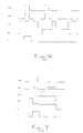
- Figs. 6 and 7 illustrate the timing operations for reading-out the image signals from the three and four-transistor black pixels 19 respectively.
- the ADC 44 of the output circuit 32 is operated at maximum analogue gain on the black pixels to convert the data to digital with maximum accuracy.
- Fig. 6 illustrates the timing operation used to read-out the image signals of the three-transistor black pixels 19 in accordance with the present invention.
- the timing operation is similar to that illustrated in Fig. 4, except the black pixel 19 is kept in minimum exposure and there is no third pulse of the second sampling switch 40.
- the same signal voltage is sampled onto both sampling capacitors 34, 36 by the first and second sampling switches 38, 40 respectively.
- any light signal which has accumulated on the black pixel 19 in the exposure time and any noise, reset or otherwise is cancelled during the analogue-to-digital conversion, which is differential.
- Fig. 7 illustrates the timing operation used to read-out the image signals of the four-transistor black pixels 19 in accordance with the present invention. Again, the timing operation is similar to that illustrated in Fig. 5, except the black pixel 19 is kept in minimum exposure and there is no second pulse the first sampling switch 38. By removing the second pulse of the first sampling switch 38, the same signal voltage is sampled onto both sampling capacitors 34, 36 by the first and second sampling switches 38, 40 respectively. Thus, any light signal which has accumulated on the black pixel 19 in the exposure time and any noise, reset or otherwise, is again cancelled during the analogue-to-digital conversion.
- black pixel data which has very low temporal noise, zero light related signal, zero dark current related signal and a common mode ADC input voltage which is equal to that of the image pixels 17.
- the common mode voltage still contains the effects of any capacitive coupling or charge injection from the falling edge of the reset signal, which should match that of the image pixels 17.
- the digital processing block 14 comprises an algorithm for removal of FPN from the digital data stream.
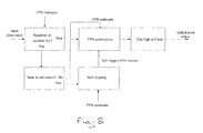
- the operations of the algorithm are performed in a learning block 50, an FPN estimate line memory block 52, an FPN estimate scaling block 54 and a subtraction block 56 of the digital processing block 14.
- the algorithm is configured to only work properly with the timing operations of Figs. 4 to 7. Also, it is important that the black pixel data is not clipped in any way during the analogue-to-digital conversion.
- the algorithm also requires a knowledge of the analogue gain being applied to the image pixels. This allows the estimate of the FPN obtained from the black pixels 19 to be scaled to match the image pixels 17 analogue gain.
- the first part of the algorithm is the calculation of the mean column-wise FPN from the black pixel data and the updating of the current FPN estimate.
- the FPN estimate line memory block 52 is cleared.
- the mean of the black pixel data is computed using: where B j is the FPN average for column j , i is the pixel in black line i for that column, P i,j is the black pixel data value and n is the number of black lines.
- the averaged FPN values for each column of black pixels 19 provides an instant estimate of the FPN.
- Equations (1) and (2) can be combined to allow only one line memory to be used in a hardware machine, giving:
- E j ( E ) The average of E j ( E ) for all the columns is computed and stored, as it is required for the cancellation part of the algorithm. This can be computed while the last black line's pixel data is added to the estimate.
- the second part of the algorithm is the cancellation of the column-wise FPN in the image signal.
- Fig. 8 illustrates the cancellation operation of the digital processing block 14.
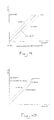
- the subtracted FPN value is scaled when cancelled by: where p saturation is the input saturation level of the data to be corrected, and k sc is the soft clipping threshold. As p i,j approaches p saturation , the FPN correction value tends to zero.
- the resulting pixel voltages above p saturation are clipped to be equal to p saturation and values below zero are clipped to zero.
- the mean luminance level of the image is not changed by the algorithm due to the mean FPN correction parameter E , so there is no interaction with the dark calibration or white balance of the image sensor 10.
- CMOS image sensor comprising column parallel analogue-to-digital converters therefore obviates or mitigates the disadvantages of previous proposals by digitally learning the FPN and subtracting this value from the image signal, and thereby removing the requirement of a frame store.
- FPN column fixed pattern noise
Landscapes
- Engineering & Computer Science (AREA)
- Multimedia (AREA)
- Signal Processing (AREA)
- Transforming Light Signals Into Electric Signals (AREA)
Abstract
Description


Claims (16)
- A method of correcting for column fixed pattern noise (FPN) in image signals obtained using an image sensor of the type comprising an image sensor array of active pixel elements arranged in rows and columns, each column having an output circuit for reading out pixel image signals comprising a pair of sample capacitors, a switching means operable in conjunction with pixel switches to apply pixel voltages to said sample capacitors, and one or more optically masked pixels such that output image signals obtained from said optically masked pixels represent substantially only the column FPN, and image processing means, comprising the steps of:(a) recording the column FPN for each column from said optically masked pixels;(b) recording the image signal from said sensor array of active pixels; and(c) subtracting the column FPN column-wise from the image signal.
- The method of Claim 1, in which step (a) comprises the steps of:(a) operating said switching means to apply a readout pixel value to both sample capacitors; and(b) utilising the difference of the resulting voltages on the capacitors as the column FPN value for each column.
- The method of Claim 2, in which the pixels are three-transistor pixels.
- The method of Claim 2, in which the pixels are four-transistor pixels.
- The method of Claim 1, in which step (a) further comprises the step of averaging and filtering the column FPN to produce an estimate of the column FPN for each column.
- The method of Claim 5, in which step (a) further comprises the step of scaling the estimate of the column FPN to match the instantaneous gain of said image sensor array of active pixels.
- The method of Claim 1, in which step (c) further comprises the step of clipping said image signal if said image signal is saturated, or close to saturation.
- The method of any preceding claim, in which the image sensor is a solid state CMOS device.
- An image sensor comprising an array of active pixel elements arranged in rows and columns, each column having an output circuit for reading out pixel image signals comprising a pair of sample capacitors, a switching means operable in conjunction with pixel switches to apply pixel voltages to said sample capacitors, one or more optically masked pixels such that output image signals obtained from said optically masked pixels represent substantially only a column fixed pattern noise (FPN), said image sensor further comprising image processing means for recording column FPN for each column from said optically masked pixels; recording the image signal from said sensor array of active pixels; and subtracting the column FPN column-wise from the image signal.
- The image sensor of Claim 9 further comprising timing means arranged to operate said switching means to apply a readout pixel value from said optically masked pixels to both sample capacitors.
- The image sensor of Claim 9, in which the pixels are three-transistor pixels.
- The image sensor of Claim 9, in which the pixels are four-transistor pixels.
- The image sensor of Claim 9, in which the image processing means is operable to average and filter said column FPN to produce an estimate of said column FPN for each column.
- The image sensor of Claim 13, in which the image processing means is operable to scale said estimate of said column FPN to match an instantaneous gain of said image sensor array of active pixels.
- The image sensor of Claim 9, in which the image processing means is operable to clip said image signal if said image signal is saturated, or close to saturation.
- The image sensor of any of Claims 9 to 15, in which the image sensor is a solid state CMOS device.
Priority Applications (3)
| Application Number | Priority Date | Filing Date | Title |
|---|---|---|---|
| EP03252872A EP1475957B1 (en) | 2003-05-08 | 2003-05-08 | Method and apparatus for removing column fixed pattern noise in solid state image sensors |
| DE60334777T DE60334777D1 (en) | 2003-05-08 | 2003-05-08 | Method and apparatus for removing fixed pitch noise in solid state image sensors |
| US10/841,947 US7801384B2 (en) | 2003-05-08 | 2004-05-07 | CMOS image sensors |
Applications Claiming Priority (1)
| Application Number | Priority Date | Filing Date | Title |
|---|---|---|---|
| EP03252872A EP1475957B1 (en) | 2003-05-08 | 2003-05-08 | Method and apparatus for removing column fixed pattern noise in solid state image sensors |
Publications (2)
| Publication Number | Publication Date |
|---|---|
| EP1475957A1 true EP1475957A1 (en) | 2004-11-10 |
| EP1475957B1 EP1475957B1 (en) | 2010-11-03 |
Family
ID=32981963
Family Applications (1)
| Application Number | Title | Priority Date | Filing Date |
|---|---|---|---|
| EP03252872A Expired - Lifetime EP1475957B1 (en) | 2003-05-08 | 2003-05-08 | Method and apparatus for removing column fixed pattern noise in solid state image sensors |
Country Status (3)
| Country | Link |
|---|---|
| US (1) | US7801384B2 (en) |
| EP (1) | EP1475957B1 (en) |
| DE (1) | DE60334777D1 (en) |
Cited By (6)
| Publication number | Priority date | Publication date | Assignee | Title |
|---|---|---|---|---|
| WO2006111472A3 (en) * | 2005-04-18 | 2007-04-05 | Imec Inter Uni Micro Electr | Sensor for eliminating undesired components and measurement method using said sensor |
| EP2015564A1 (en) * | 2007-07-12 | 2009-01-14 | Canon Kabushiki Kaisha | Imaging apparatus and its control method |
| EP2337338A1 (en) * | 2009-11-30 | 2011-06-22 | STMicroelectronics (Research & Development) Limited | Method and system for x-droop correction in solid state image sensor |
| WO2011081962A1 (en) * | 2009-12-31 | 2011-07-07 | Omnivision Technologies, Inc. | Generating column offset corrections for image sensors |
| WO2011081959A1 (en) * | 2009-12-31 | 2011-07-07 | Omnivision Technologies, Inc. | Generating column offset corrections for image sensors |
| US8269864B2 (en) | 2009-12-31 | 2012-09-18 | Omnivision Technologies, Inc. | Generating column offset corrections for image sensors |
Families Citing this family (16)
| Publication number | Priority date | Publication date | Assignee | Title |
|---|---|---|---|---|
| JP2006098217A (en) * | 2004-09-29 | 2006-04-13 | Fujitsu Ltd | Image inspection apparatus, image inspection method, and image inspection program |
| KR100734288B1 (en) * | 2005-11-17 | 2007-07-02 | 삼성전자주식회사 | Initial charge supply method of the CIS circuit and the CIS circuit |
| US8310569B2 (en) * | 2007-05-21 | 2012-11-13 | Aptina Imaging Corporation | Suppression of row-wise noise in CMOS image sensors |
| US20090021623A1 (en) * | 2007-07-18 | 2009-01-22 | Micron Technology, Inc. | Systems, methods and devices for a CMOS imager having a pixel output clamp |
| US20090040351A1 (en) * | 2007-08-09 | 2009-02-12 | Micron Technology, Inc. | Method and apparatus for reducing noise in a pixel array |
| JP5124416B2 (en) * | 2008-10-14 | 2013-01-23 | Hoya株式会社 | Fixed pattern noise elimination unit, imaging unit, and electronic endoscope system |
| GB0920921D0 (en) | 2009-11-30 | 2010-01-13 | St Microelectronics Res & Dev | Method and system for repeated fixed patttern noise correction |
| JP5627275B2 (en) * | 2010-04-21 | 2014-11-19 | キヤノン株式会社 | Image processing apparatus, image processing method, and program |
| US8724002B2 (en) | 2011-02-28 | 2014-05-13 | Aptina Imaging Corporation | Imaging pixels with dummy transistors that reduce reset charge injection |
| JP6164869B2 (en) * | 2013-02-26 | 2017-07-19 | キヤノン株式会社 | Imaging device, imaging system, and driving method of imaging device |
| JP6418839B2 (en) * | 2014-08-04 | 2018-11-07 | キヤノン株式会社 | Imaging apparatus, control method therefor, program, and storage medium |
| CN109829866B (en) * | 2019-02-01 | 2021-02-19 | 安谋科技(中国)有限公司 | Column noise detection method, apparatus, medium, and system |
| TWI795803B (en) * | 2021-06-11 | 2023-03-11 | 瑞鼎科技股份有限公司 | Image sensor |
| CA3227077A1 (en) * | 2021-08-11 | 2023-02-16 | Ryan KLEBBA | Dynamic fixed pattern noise calibrations |
| EP4441199A4 (en) * | 2021-12-01 | 2025-05-07 | Life Technologies Corporation | SYSTEMS, APPARATUSES AND METHODS FOR MITIGATING THE EFFECT OF FLUID POTENTIAL IN LARGE-SCALE CHEMFET ARRAYS |
| CN117097335B (en) * | 2023-10-18 | 2024-01-26 | 南京天易合芯电子有限公司 | High-sensitivity proximity light detection sensor |
Citations (2)
| Publication number | Priority date | Publication date | Assignee | Title |
|---|---|---|---|---|
| US6061092A (en) * | 1997-12-05 | 2000-05-09 | Intel Corporation | Method and apparatus for dark frame cancellation for CMOS sensor-based tethered video peripherals |
| GB2375252A (en) * | 2000-08-18 | 2002-11-06 | Sgs Thomson Microelectronics | Reduction of column fixed pattern noise in image sensors |
Family Cites Families (13)
| Publication number | Priority date | Publication date | Assignee | Title |
|---|---|---|---|---|
| US4392157A (en) * | 1980-10-31 | 1983-07-05 | Eastman Kodak Company | Pattern noise reduction method and apparatus for solid state image sensors |
| US5471515A (en) * | 1994-01-28 | 1995-11-28 | California Institute Of Technology | Active pixel sensor with intra-pixel charge transfer |
| US6166768A (en) * | 1994-01-28 | 2000-12-26 | California Institute Of Technology | Active pixel sensor array with simple floating gate pixels |
| US5604601A (en) * | 1994-08-24 | 1997-02-18 | International Business Machines Corporation | Reference grid rectilinear correction |
| US5572608A (en) * | 1994-08-24 | 1996-11-05 | International Business Machines Corporation | Sinc filter in linear lumen space for scanner |
| US5608538A (en) * | 1994-08-24 | 1997-03-04 | International Business Machines Corporation | Scan line queuing for high performance image correction |
| US5987156A (en) * | 1996-11-25 | 1999-11-16 | Lucent Technologies | Apparatus for correcting fixed column noise in images acquired by a fingerprint sensor |
| US6606122B1 (en) * | 1997-09-29 | 2003-08-12 | California Institute Of Technology | Single chip camera active pixel sensor |
| DE19746623C1 (en) * | 1997-10-22 | 1998-11-19 | Siemens Ag | Method of determining line correction values for medical digital image converter |
| US6160282A (en) * | 1998-04-21 | 2000-12-12 | Foveon, Inc. | CMOS image sensor employing silicide exclusion mask to reduce leakage and improve performance |
| US6476864B1 (en) * | 1998-05-11 | 2002-11-05 | Agilent Technologies, Inc. | Pixel sensor column amplifier architecture |
| US6101287A (en) * | 1998-05-27 | 2000-08-08 | Intel Corporation | Dark frame subtraction |
| US6670598B1 (en) * | 2000-09-06 | 2003-12-30 | Xerox Corporation | Low power autozero of pixel amplifier |
-
2003
- 2003-05-08 DE DE60334777T patent/DE60334777D1/en not_active Expired - Lifetime
- 2003-05-08 EP EP03252872A patent/EP1475957B1/en not_active Expired - Lifetime
-
2004
- 2004-05-07 US US10/841,947 patent/US7801384B2/en not_active Expired - Fee Related
Patent Citations (2)
| Publication number | Priority date | Publication date | Assignee | Title |
|---|---|---|---|---|
| US6061092A (en) * | 1997-12-05 | 2000-05-09 | Intel Corporation | Method and apparatus for dark frame cancellation for CMOS sensor-based tethered video peripherals |
| GB2375252A (en) * | 2000-08-18 | 2002-11-06 | Sgs Thomson Microelectronics | Reduction of column fixed pattern noise in image sensors |
Cited By (14)
| Publication number | Priority date | Publication date | Assignee | Title |
|---|---|---|---|---|
| WO2006111472A3 (en) * | 2005-04-18 | 2007-04-05 | Imec Inter Uni Micro Electr | Sensor for eliminating undesired components and measurement method using said sensor |
| US8423105B2 (en) | 2005-04-18 | 2013-04-16 | Imec | Sensor for eliminating undesired components and measurements method using said sensor |
| EP2015564A1 (en) * | 2007-07-12 | 2009-01-14 | Canon Kabushiki Kaisha | Imaging apparatus and its control method |
| US7999864B2 (en) | 2007-07-12 | 2011-08-16 | Canon Kabushiki Kaisha | Imaging apparatus and its control method for setting suitable clipping level |
| EP2337338A1 (en) * | 2009-11-30 | 2011-06-22 | STMicroelectronics (Research & Development) Limited | Method and system for x-droop correction in solid state image sensor |
| US8462235B2 (en) | 2009-11-30 | 2013-06-11 | Stmicroelectronics (Research & Development) Limited | Method and system for X-droop correction in solid state image sensor |
| US8199225B2 (en) | 2009-12-31 | 2012-06-12 | Omnivision Technologies, Inc. | Generating column offset corrections for image sensors |
| US8228403B2 (en) | 2009-12-31 | 2012-07-24 | Omnivision Technologies, Inc. | Generating column offset corrections for image sensors |
| US8269864B2 (en) | 2009-12-31 | 2012-09-18 | Omnivision Technologies, Inc. | Generating column offset corrections for image sensors |
| CN102714703A (en) * | 2009-12-31 | 2012-10-03 | 全视科技有限公司 | Generating column offset corrections for image sensors |
| WO2011081959A1 (en) * | 2009-12-31 | 2011-07-07 | Omnivision Technologies, Inc. | Generating column offset corrections for image sensors |
| WO2011081962A1 (en) * | 2009-12-31 | 2011-07-07 | Omnivision Technologies, Inc. | Generating column offset corrections for image sensors |
| TWI454143B (en) * | 2009-12-31 | 2014-09-21 | Omnivision Tech Inc | Method for determining column offset corrections for image sensors |
| CN102714703B (en) * | 2009-12-31 | 2015-02-18 | 全视科技有限公司 | Generating column offset corrections for image sensors |
Also Published As
| Publication number | Publication date |
|---|---|
| DE60334777D1 (en) | 2010-12-16 |
| EP1475957B1 (en) | 2010-11-03 |
| US20050104981A1 (en) | 2005-05-19 |
| US7801384B2 (en) | 2010-09-21 |
Similar Documents
| Publication | Publication Date | Title |
|---|---|---|
| EP1475957B1 (en) | Method and apparatus for removing column fixed pattern noise in solid state image sensors | |
| US9554071B2 (en) | Method and apparatus providing pixel storage gate charge sensing for electronic stabilization in imagers | |
| US6344877B1 (en) | Image sensor with dummy pixel or dummy pixel array | |
| US6067113A (en) | Offset noise cancellation in array image sensors | |
| US8586907B2 (en) | Methods of operating an imaging pixel to accumulate charge from a photocurrent | |
| US10116890B2 (en) | Imaging apparatus and imaging method using difference between reset signal and pixel signal stored to two capacitors | |
| US7633541B2 (en) | Image pickup apparatus having a correction unit for a digital image signal | |
| US8334917B2 (en) | Ultra low noise CMOS imager | |
| US7623164B2 (en) | Image sensing apparatus and method for accurate dark current recovery of an image signal | |
| US6275259B1 (en) | Digital automatic gain control circuit for image system | |
| US10033956B2 (en) | Image sensor | |
| US11284025B2 (en) | Digital pixel having high sensitivity and dynamic range | |
| US20030231252A1 (en) | Image sensor with improved noise cancellation | |
| CN106454156B (en) | Image sensor and method of operation | |
| US7242429B1 (en) | Method for cancellation of the effect of charge feedthrough on CMOS pixel output | |
| EP1725019A2 (en) | On chip real time FPN correction without imager size memory | |
| JP2003259234A (en) | CMOS image sensor | |
| JP6723736B2 (en) | Imaging device, imaging system, and method of driving imaging device | |
| JP2006148455A (en) | Solid imaging apparatus | |
| US20240196110A1 (en) | Cmos image sensor for rts noise reduction using non-linear statistics and impulsive metrics for signal processing | |
| JP2006303692A (en) | Image signal processing circuit and electronic camera | |
| JP2005020680A (en) | Image sensor output correction device | |
| JPH0937107A (en) | Image pickup signal corrector |
Legal Events
| Date | Code | Title | Description |
|---|---|---|---|
| PUAI | Public reference made under article 153(3) epc to a published international application that has entered the european phase |
Free format text: ORIGINAL CODE: 0009012 |
|
| AK | Designated contracting states |
Kind code of ref document: A1 Designated state(s): AT BE BG CH CY CZ DE DK EE ES FI FR GB GR HU IE IT LI LU MC NL PT RO SE SI SK TR |
|
| AX | Request for extension of the european patent |
Extension state: AL LT LV MK |
|
| 17P | Request for examination filed |
Effective date: 20050426 |
|
| AKX | Designation fees paid |
Designated state(s): DE FR GB IT |
|
| RAP1 | Party data changed (applicant data changed or rights of an application transferred) |
Owner name: STMICROELECTRONICS (RESEARCH & DEVELOPMENT) LIMITE |
|
| 17Q | First examination report despatched |
Effective date: 20090909 |
|
| GRAP | Despatch of communication of intention to grant a patent |
Free format text: ORIGINAL CODE: EPIDOSNIGR1 |
|
| GRAS | Grant fee paid |
Free format text: ORIGINAL CODE: EPIDOSNIGR3 |
|
| GRAA | (expected) grant |
Free format text: ORIGINAL CODE: 0009210 |
|
| AK | Designated contracting states |
Kind code of ref document: B1 Designated state(s): DE FR GB IT |
|
| REG | Reference to a national code |
Ref country code: GB Ref legal event code: FG4D |
|
| REF | Corresponds to: |
Ref document number: 60334777 Country of ref document: DE Date of ref document: 20101216 Kind code of ref document: P |
|
| PLBE | No opposition filed within time limit |
Free format text: ORIGINAL CODE: 0009261 |
|
| STAA | Information on the status of an ep patent application or granted ep patent |
Free format text: STATUS: NO OPPOSITION FILED WITHIN TIME LIMIT |
|
| 26N | No opposition filed |
Effective date: 20110804 |
|
| REG | Reference to a national code |
Ref country code: DE Ref legal event code: R097 Ref document number: 60334777 Country of ref document: DE Effective date: 20110804 |
|
| PG25 | Lapsed in a contracting state [announced via postgrant information from national office to epo] |
Ref country code: IT Free format text: LAPSE BECAUSE OF FAILURE TO SUBMIT A TRANSLATION OF THE DESCRIPTION OR TO PAY THE FEE WITHIN THE PRESCRIBED TIME-LIMIT Effective date: 20101103 |
|
| REG | Reference to a national code |
Ref country code: FR Ref legal event code: ST Effective date: 20120131 |
|
| PG25 | Lapsed in a contracting state [announced via postgrant information from national office to epo] |
Ref country code: FR Free format text: LAPSE BECAUSE OF NON-PAYMENT OF DUE FEES Effective date: 20110531 |
|
| PGFP | Annual fee paid to national office [announced via postgrant information from national office to epo] |
Ref country code: DE Payment date: 20120423 Year of fee payment: 10 |
|
| PGFP | Annual fee paid to national office [announced via postgrant information from national office to epo] |
Ref country code: GB Payment date: 20120423 Year of fee payment: 10 |
|
| GBPC | Gb: european patent ceased through non-payment of renewal fee |
Effective date: 20130508 |
|
| PG25 | Lapsed in a contracting state [announced via postgrant information from national office to epo] |
Ref country code: DE Free format text: LAPSE BECAUSE OF NON-PAYMENT OF DUE FEES Effective date: 20131203 |
|
| REG | Reference to a national code |
Ref country code: DE Ref legal event code: R119 Ref document number: 60334777 Country of ref document: DE Effective date: 20131203 |
|
| PG25 | Lapsed in a contracting state [announced via postgrant information from national office to epo] |
Ref country code: GB Free format text: LAPSE BECAUSE OF NON-PAYMENT OF DUE FEES Effective date: 20130508 |