BACKGROUND OF THE INVENTION
1. FEILD OF THE INVENTION
-
The present invention relates to an image display control
method for use in a liquid crystal display apparatus, a plasma
display apparatus, an EL (electro-luminescence) display
apparatus and the like to display images, and to an image display
control apparatus.
2. PRIOR ART
-
As conventional techniques regarding an image display
control method and an image display control apparatus, a liquid
crystal display control method and a liquid crystal display
control apparatus will now be described.
-
Fig. 4 is a schematic block diagram of a conventional
liquid crystal display control apparatus as it handles a liquid
crystal display (image display) request and a host computer
access request. In Fig. 4, denoted at 401 is a host computer,
namely, a micro computer unit. Denoted at 402 is a host
interface circuit. Denoted at 403 is a memory circuit which
stores display data. Denoted at 404 is a line latch circuit
which stores one horizontal line-equivalent display data which
is used to realize liquid crystal display (image display).
Denoted at 405 is a memory select address location which is in
response to a host access. Denoted at 406 is a memory line
select address location which is in response to an LCD display
read access. Denoted at 407 is a display line data transfer
signal for an LCD display read access.
-
As the host computer 401 accesses in order to write display
data, pixel data is written at the memory address select
location 405 which corresponds to a vertical-direction and a
horizontal-direction addresses within the memory circuit 403.
Meanwhile, since display data one horizontal line equivalent
to needs be transferred to the line latch circuit 404 to realize
liquid crystal display (image display), a vertical address
corresponding to one horizontal line is selected from among
addresses within the memory circuit 403 in accordance with the
memory line select address location 406 which is in response
to the LCD display read access. The data representing thus
selected line is sent to the line latch circuit 404 based on
the display line data transfer signal 407.
-
An access request to the memory circuit 403 from the host
computer 401 is in an asynchronous relationship with an access
request to the memory circuit 403 from the liquid crystal
display apparatus. Hence, while the host computer 401 and the
liquid crystal display apparatus both access, the same data
address could be selected.
-
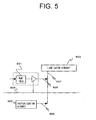
Fig. 5 is a schematic diagram showing an example of a 1-bit
structure within a memory circuit and a relationship with a line
latch circuit. In Fig. 5, denoted at 501 is a 1-bit memory.
Denoted at 502 is an initialization circuit. Denoted at 503
is a line latch circuit. Denoted at 504 is a line select signal.
Denoted at 505 is a memory output. Denoted at 506 is an output
from the initialization circuit 502. Denoted at 507 is a
display read bus.
-
The 1-bit memory 501 within the memory circuit is formed
by a P-channel or N-channel transistor for a small size. Within
the memory circuit, a display read operation for a line selected
by the line select signal 504 is as follows. That is, the
display read bus 507 is initialized in response to the
initialization output 506 from the initialization circuit 502,
the memory output 505 from the 1-bit memory 501 is then outputted
to the display read bus 507, and the line latch circuit 503
receives OR of the initialization output 506 and the memory
output 505. When a P-channel transistor is used for example,
the memory output 505, namely, read data is in a high-level state
or high-impedance state, and therefore, the initialization
circuit 502 reads the L-level.
-
Figs. 6 and 7 are timing charts which show an example that
there is no contention between an access request from the host
computer and an access request for liquid crystal display (image
display) and an example that there is such a contention.
-
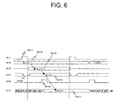
Shown in Fig. 6 is a normal state that there is no
contention between a host computer access and a display read
access. In Fig. 6, a high-level pulse T611 occurs in a display
read signal 611, at which time a value T612 (00_1111) of memory
data 612 changes to a value T613 (00_1111) of a display read
data output 613 from the memory circuit. Meanwhile, the pulse
T611 of the display read signal 611 makes the initialization
circuit execute initialization, and the state of a display read
bus 614 therefore becomes an initialized state T614.
-
After this, because of the value T613 of the display read
data output 613, the state of the display read bus 614 becomes
a value T615 (00_1111). As a high-level pulse T616 occurs in
a display line data transfer signal 616, a line latch output
617 becomes a value T617 (00_1111).
-
Fig. 7 shows a state that there arises a contention between
a host computer access and a display read access. As shown in
Fig. 7, a high-level pulse T621 occurs in a display read signal
621, at which time a value T622 (00_1111) of memory data 622
changes to a value T623 (00_1111) of a display read data output
623 from the memory circuit. Meanwhile, the pulse T621 of the
display read signal 621 makes the initialization circuit
execute initialization, and the state of a display read bus 624
therefore becomes an initialized state T624.
-
After this, because of the value T623 of the display read
data output 623, the state of the display read bus 624 becomes
a value T625 (00_1111).
-
When the memory data 622 changes to a value T626 (00_1111)
owing to a host computer access during a contending data display
period T631 which is influenced by the access contention, the
display read data output 623 from the memory circuit becomes
a value T627 (00_1111). In consequence, the state of a display
read bus 624 undesirably becomes a value T628 (11_1111) which
is OR of the value T625 (00_1111) and the value T627 (00_1111).
As a high-level pulse T629 occurs in a display line data transfer
signal 629, a line latch output 630 undesirably becomes a value
T630 (11_1111) which is influenced by the access contention.
-
The following may be a method of avoiding an access
contention in a situation that an access to the memory circuit
from the host computer is in an asynchronous relationship with
a display read access to the memory circuit from the liquid
crystal display apparatus. In other words, when the host
computer sends an access request while the liquid crystal
display apparatus sends an LCD access request, an arbitration
circuit may provide arbitration and RAM accessing responding
to either one of the access requests may be initiated. At this
stage, the arbitration circuit permits initiation of accessing
under a condition that pre-charging of the RAM has finished.
When there is a contention between a host access request and
an LCD access request, the host access request is always given
a priority (See PCT Publication in Japan 2000-003381 (page 1,
Fig. 2).). The arbitration circuit may be the one described
in Japanese Patent Application Laid-Open Gazette No. H10-105505
(pages 6 to 8, Fig. 5), for instance.
-
However, during the arbitration in the conventional
structure described above, when a display read access from the
liquid crystal display apparatus is earlier than a write access
from the host computer for example, displaying will be provided
before the arbitration circuit stops display read. There thus
remains a problem that the contending data will be displayed.
-
In addition, when a contention with a host access arises
once again upon resumption of an LCD access in response to an
operation of the arbitration circuit, the arbitration will
continue. This is a problem that displaying will not be
provided indefinitely or that the complex arbitration circuit
gives rise to malfunction.
SUMMARY OF THE INVENTION
-
An object of the present invention is to provide an image
display control method and an image display control apparatus
with which it is possible to prevent displaying of wrong data
on a screen owing to a contention between a write access from
a host computer and a display read access from an image display
apparatus.
-
The image display control method and the image display
control apparatus according to the present invention determine
that a period of time which is influenced by a contention is
an access contention monitoring period and require that upon
detection of a contention during this period, a display read
signal and a display line data transfer signal are generated
as a pair at the stage of writing in a memory circuit. This
makes it possible to always transfer the most recent information
of a memory to a line latch circuit so that the information will
be displayed.
-
As another means, a period of time which is influenced
by a contention is regarded as an access contention monitoring
period, and when a contention is detected during this period,
same line re-display read processing is executed immediately
after the detection of the contention. This makes wrong display
data overwritten as a result of the re-display processing every
time a contention occurs, and hence, the contending display data
are made invisible.
-
An image display control method according to the first
invention requires that display data written in a memory circuit
(120) is read in the units of lines and held in a line latch
circuit (121), the display data is supplied in the units of lines
to an image display apparatus from the line latch circuit (121)
and the image display apparatus accordingly displays an image.
At this stage, an access contention for the same address in the
memory circuit (120) is to be detected which occurs between
writing to update the display data and reading of the display
data to display an image. In the event that an access contention
is detected, a display read signal and a display line data
transfer signal are generated based on a memory write clock,
and the display read signal and the display line data transfer
signal are supplied to the memory circuit (120) while supplying
the display line data transfer signal to the line latch circuit
(121) which holds, in the units of lines, data which has been
read out from the memory circuit (120). In consequence, the
display data representing the line for which the access
contention has occurred is read out from the memory circuit
(120) and transferred to the line latch circuit (121).
-
In accordance with this method, when an access contention
to the same address within the memory circuit (120) is detected
between writing for updating of display data and reading of
display data for displaying of an image, that is, when a
contention is detected between a memory write address and a
display read address in the memory circuit (120), the display
read signal and the display line data transfer signal are
generated based on the memory write clock, the display read
signal and the display line data transfer signal are then fed
to the memory circuit (120) while supplying the display line
data transfer signal also to the line latch circuit (121). The
display data is therefore read out from the memory circuit (120)
as for the access contention-bearing line and transferred to
the line latch circuit (121). This prevents displaying of wrong
data on a screen which would be otherwise caused by the
contention between the write access from the host computer and
the display read access from the image display apparatus.
-
In the image display control method according to the first
invention, it is preferable that the display read signal and
the display line data transfer signal are generated as a pair
based on the memory write clock and outputted to the memory
circuit (120) for every contention, and at the time of writing
of display data in the memory circuit (120), the latest updated
data is always re-transferred to the line latch circuit (121).
-
When this method is used, it is possible to more securely
prevent displaying of wrong data on a screen attributed to the
contention between the write access from the host computer and
the display read access from the image display apparatus.
-
An image display control method according to the second
invention requires that display data written in a memory circuit
(120) is read in the units of lines and held in a line latch
circuit (121) , the display data is supplied in the units of lines
to an image display apparatus from the line latch circuit (121)
and the image display apparatus accordingly displays an image.
At this stage, an access contention for the same address in the
memory circuit (120) is to be detected which occurs between
writing to update the display data and reading of the display
data to display an image. In the event that an access contention
is detected, a display read signal and a display line data
transfer signal are generated for execution of same line
re-display read processing, and the display read signal and the
display line data transfer signal are supplied to the memory
circuit (120) while supplying the display line data transfer
signal to the line latch circuit (121) which holds, in the units
of lines, data which has been read out from the memory circuit
(120) . In consequence, the line for which the access contention
has occurred is re-displayed.
-
In accordance with this method, when an access contention
to the same address within the memory circuit (120) is detected
between writing for updating of display data and reading of
display data for displaying of an image, that is, when a
contention is detected between a memory write address and a
display read address in the memory circuit (120), the display
read signal and the display line data transfer signal are
generated for execution of the same line re-display read
processing without moving to the next line, the display read
signal and the display line data transfer signal are then fed
to the memory circuit (120) while supplying the display line
data transfer signal also to the line latch circuit (121) in
which data read out from the memory circuit (120) are held line
by line. The line for which the contention has occurred is thus
re-displayed. This prevents displaying of wrong data on a
screen which would be otherwise caused by the contention between
the write access from the host computer and the display read
access from the image display apparatus.
-
In the image display control method of the second
invention, it is preferable that the same line is re-displayed
speedily upon occurrence of a contention, and therefore,
without displaying wrong data because of the access contention,
the latest data held in the memory circuit (120) is
re-transferred to the line latch circuit (121) and the latest
data as it is after the contention has been resolved is
displayed.
-
By means of this method, it is possible to more securely
prevent displaying of wrong data on a screen attributed to the
contention between the write access from the host computer and
the display read access from the image display apparatus.
-
In the image display control method above, the number of
times for re-displaying the same line can be freely set.
-
When this method is used, it is possible to execute the
re-display processing indefinitely, or alternatively, by
setting the number of times and accordingly limiting the
re-display processing to a certain range which will maintain
a display quality, it is possible to suppress a drop of the frame
frequency of a display image.
-
Because of the re-display processing, this line is
extended in terms of time to normal one-line display time + α
(i.e., the time before proceeding to re-displaying). Since a
contention could possibly arise again for every re-display
processing, if the re-display processing lasts long, the same
line will be displayed indefinitely and the display image will
remain as a still image indefinitely. The number of times
mentioned above is set so as to avoid this, and the number of
times may be set within the range which will maintain a display
quality.
-
In the image display control method of the second
invention, it is preferable that the same line is re-displayed
so that the phase relationship is forced to shift between the
cycles of display data transfer to the memory circuit (120) and
the cycles of a display read access to the memory circuit (120)
and that the frequency of later access contentions for the same
address is accordingly reduced.
-
An image display control apparatus according to the third
invention comprises: a host computer (101);
a host interface circuit (102) which transfers display
data with the host computer (101);
a memory address counter circuit (103) which receives a
write address from the host interface circuit (102) and
increments or decrements the address;
a register setting circuit (104) which receives a
register write address and register write data from the host
interface circuit (102);
a display read clock signal generating circuit (105)
which generates a display read clock signal which serves as a
reference clock for displaying;
a horizontal-direction counter circuit (106) for display
which counts the display read clock signal which is outputted
from the display read clock signal generating circuit (105);
a horizontal-counter decode circuit (107) which decodes
an output signal of the horizontal-direction counter circuit
for display (106) and outputs a first display read signal and
a first display line data transfer signal;
a vertical-direction counter circuit for display (108)
which receives a predetermined output value of the
horizontal-direction counter circuit for display (106) and
increments or decrements;
a counter decode circuit (109) which decodes an output
from the vertical-direction counter circuit for display (108)
and an output from the memory address counter circuit (103) and
outputs a memory write address and a display read address;
an address coincidence detect circuit (110) which
receives the memory write address and the display read address
which are outputted from the counter decode circuit (109) and
determines whether the memory write address and the display read
address coincide with each other;
an access contention monitoring period pulse generating
circuit (111) which generates a pulse which defines an access
contention monitoring period, based on the outputs from the
horizontal-counter decode circuit (107);
an address contention judging circuit (112) which
determines whether there is a contention between the display
read address and the memory write address in accordance with
an output from the address coincidence detect circuit (110) and
an output from the access contention monitoring period pulse
generating circuit (111);
a host retry pulse generating circuit (113) which
receives the memory write clock from the host interface circuit
(102) and an output from the address contention judging circuit
(112), and during the access contention monitoring period, as
an access contention arises, generates a second display read
signal and a second display line data transfer signal based on
the memory write clock;
a normal read processing circuit (115) which generates
a third display read signal and a third display line data
transfer signal which are for execution of normal display read
processing, in accordance with the first display read signal
and the first display line data transfer signal outputted from
the horizontal-counter decode circuit (107) and the output from
the vertical-direction counter circuit for display (108);
a retry display read selection circuit (118) which
selectively outputs, in accordance with an output from the
register setting circuit (104), either one of the second display
read signal outputted from the host retry pulse generating
circuit (113) and the third display read signal outputted from
the normal read processing circuit (115);
a retry line data transfer selection circuit (119) which
selectively outputs, in accordance with an output from the
register setting circuit (104), either one of the second display
line data transfer signal outputted from the host retry pulse
generating circuit (113) and the third display line data
transfer signal outputted from the normal read processing
circuit (115);
a memory circuit (120) which receives an output from the
host interface circuit (102), an output from the memory address
counter circuit (103), an output from the vertical-direction
counter circuit for display (108), an output from the retry
display read selection circuit (118) and an output from the
retry line data transfer selection circuit (119), and stores
display data which a image display apparatus is to display;
and a line latch circuit (121) which receives an output
from the memory circuit (120) and the output from the retry line
data transfer selection circuit (119), holds the output from
the memory circuit (120) in the units of lines, and supplies
an output to the image display apparatus.
-
This structure comprises the address coincidence detect
circuit (110), the access contention monitoring period pulse
generating circuit (111), the address contention judging
circuit (112) and the host retry pulse generating circuit (113).
When a contention arises between a memory write address and a
display read address in the memory circuit (120), that is, when
an access contention to the same address within the memory
circuit (120) is detected between writing for updating of
display data and reading of display data for displaying of an
image, the second display read signal and the second display
line data transfer signal are generated based on the memory
write clock, the second display read signal and the second
display line data transfer signal are then fed to the memory
circuit (120) while supplying the second display line data
transfer signal also to the line latch circuit (121) in which
data read out from the memory circuit (120) are held line by
line. This makes it possible to read display data representing
the access contention-bearing line out from the memory circuit
(120) and transfer the display data to the line latch circuit
(121). As a result, it is possible to prevent displaying of
wrong data on a screen which would be otherwise caused by the
contention between the write access from the host computer and
the display read access from the image display apparatus.
-
An image display control apparatus of the fourth
invention comprises: a host computer (101);
a host interface circuit (102) which transfers display
data with the host computer (101);
a memory address counter circuit (103) which receives a
write address from the host interface circuit (102) and
increments or decrements the address;
a register setting circuit (104) which receives a
register write address and register write data from the host
interface circuit (102);
a display read clock signal generating circuit (105)
which generates a display read clock signal which serves as a
reference clock for displaying;
a horizontal-direction counter circuit for display (106)
which counts the display read clock signal which is outputted
from the display read clock signal generating circuit (105);
a horizontal-counter decode circuit (107) which decodes
an output signal of the horizontal-direction counter circuit
for display (106) and outputs a first display read signal and
a first display line data transfer signal;
a vertical-direction counter circuit for display (108)
which receives a predetermined output value of the
horizontal-direction counter circuit for display (106) and
increments or decrements;
a counter decode circuit (109) which decodes an output
from the vertical-direction counter circuit for display (108)
and an output from the memory address counter circuit (103) and
outputs a memory write address and a display read address;
an address coincidence detect circuit (110) which
receives the memory write address and the display read address
which are outputted from the counter decode circuit (109) and
determines whether the memory write address and the display read
address coincide with each other;
an access contention monitoring period pulse generating
circuit (111) which generates a pulse which defines an access
contention monitoring period, based on the outputs from the
horizontal-counter decode circuit (107);
an address contention judging circuit (112) which
determines whether there is a contention between the display
read address and the memory write address in accordance with
an output from the address coincidence detect circuit (110) and
an output from the access contention monitoring period pulse
generating circuit (111);
a same line re-display read processing circuit (114)
which receives the first display read signal and the first
display line data transfer signal outputted from the
horizontal-counter decode circuit (107) and an output from the
address contention judging circuit (112), and generates a
second display read signal and a second display line data
transfer signal which are for execution of same line re-display
read processing, without moving to the next line as a contention
arises during the access contention monitoring period;
a normal read processing circuit (115) which generates
a third display read signal and a third display line data
transfer signal which are for execution of normal display read
processing, in accordance with the first display read signal
and the first display line data transfer signal outputted from
the horizontal-counter decode circuit (107) and the output from
the vertical-direction counter circuit for display (108);
a retry display read selection circuit (118) which
selectively outputs, in accordance with an output from the
register setting circuit (104) , either one of the second display
read signal outputted from the same line re-display read
processing circuit (114) and the third display read signal
outputted from the normal read processing circuit (115);
a retry line data transfer selection circuit (119) which
selectively outputs, in accordance with an output from the
register setting circuit (104) , either one of the second display
line data transfer signal outputted from the same line
re-display read processing circuit (114)and the third display
line data transfer signal outputted from the normal read
processing circuit (115);
a memory circuit (120) which receives an output from the
host interface circuit (102), an output from the memory address
counter circuit (103), an output from the vertical-direction
counter circuit for display (108), an output from the retry
display read selection circuit (118) and an output from the
retry line data transfer selection circuit (119), and stores
display data which a image display apparatus is to display; and
a line latch circuit (121) which receives an output from
the memory circuit (120) and the output from the retry line data
transfer selection circuit (119), holds the output from the
memory circuit (120) in the units of lines, and supplies an
output to the image display apparatus.
-
This structure comprises the address coincidence detect
circuit (110), the access contention monitoring period pulse
generating circuit (111), the address contention judging
circuit (112) and the same line re-display read processing
circuit (114). When a contention arises between a memory write
address and a display read address in the memory circuit (120),
that is, when an access contention to the same address within
the memory circuit (120) is detected between writing for
updating of display data and reading of display data for
displaying of an image, the second display read signal and the
second display line data transfer signal are generated for
execution of the same line re-display read processing without
moving to the next line, the second display read signal and the
second display line data transfer signal are then fed to the
memory circuit (120) while supplying the second display line
data transfer signal also to the line latch circuit (121) in
which data read out from the memory circuit (120) are held line
by line. The line for which the contention has occurred is thus
re-displayed. This prevents displaying of wrong data on a
screen which would be otherwise caused by the contention between
the write access from the host computer and the display read
access from the image display apparatus.
-
An image display control apparatus of the fifth invention
comprises: a host computer (101);.
a host interface circuit (102) which transfers display
data with the host computer (101);
a memory address counter circuit (103) which receives a
write address from the host interface circuit (102) and
increments or decrements the address;
a register setting circuit (104) which receives a
register write address and register write data from the host
interface circuit (102);
a display read clock signal generating circuit (105)
which generates a display read clock signal which serves as a
reference clock for displaying;
a horizontal-direction counter circuit (106) for display
which counts the display read clock signal which is outputted
from the display read clock signal generating circuit (105);
a horizontal-counter decode circuit (107) which decodes
an output signal of the horizontal-direction counter circuit
for display (106) and outputs a first display read signal and
a first display line data transfer signal;
a vertical-direction counter circuit for display (108)
which receives a predetermined output value of the
horizontal-direction counter circuit for display (106) and
increments or decrements;
a counter decode circuit (109) which decodes an output
from the vertical-direction counter circuit for display (108)
and an output from the memory address counter circuit (103) and
outputs a memory write address and a display read address;
an address coincidence detect circuit (110) which
receives the memory write address and the display read address
which are outputted from the counter decode circuit (109) and
determines whether the memory write address and the display read
address coincide with each other;
an access contention monitoring period pulse generating
circuit (111) which generates a pulse which defines an access
contention monitoring period, based on the outputs from the
horizontal-counter decode circuit (107);
an address contention judging circuit (112) which
determines whether there is a contention between the display
read address and the memory write address in accordance with
an output from the address coincidence detect circuit (110) and
an output from the access contention monitoring period pulse
generating circuit (111);
a host retry pulse generating circuit (113) which
receives the memory write clock from the host interface circuit
(102) and an output from the address contention judging circuit
(112), and during the access contention monitoring period, as
an access contention arises, generates a second display read
signal and a second display line data transfer signal based on
the memory write clock;
a same line re-display read processing circuit (114)
which receives the first display read signal and the first
display line data transfer signal outputted from the
horizontal-counter decode circuit (107) and an output from the
address contention judging circuit (112) , and generates a third
display read signal and a third display line data transfer
signal which are for execution of same line re-display read
processing, without moving to the next line as a contention
arises during the access contention monitoring period;
a normal read processing circuit (115) which generates
a fourth display read signal and a fourth display line data
transfer signal which are for execution of normal display read
processing, in accordance with the first display read signal
and the first display line data transfer signal outputted from
the horizontal-counter decode circuit (107) and the output from
the vertical-direction counter circuit for display (108);
a display read selection circuit (116) which selects, in
accordance with an output from the register setting circuit
(104), either a state that of the second display read signal
outputted from the host retry pulse generating circuit (113)
and the third display read signal outputted from the same line
re-display read processing circuit (114), only the second
display read signal outputted from the host retry pulse
generating circuit (113) is outputted, a state that the third
display read signal outputted from the same line re-display read
processing circuit (114) alone out of these is outputted, or
a state that both the second display read signal outputted from
the host retry pulse generating circuit (113) and the third
display read signal outputted from the same line re-display read
processing circuit (114) are made valid and outputted, and which
outputs this as a fifth display read signal;
a line data transfer selection circuit (117) which
selects, in accordance with an output from the register setting
circuit (104), either a state that of the second display line
data transfer signal outputted from the host retry pulse
generating circuit (113) and the third display line data
transfer signal outputted from the same line re-display read
processing circuit (114), only the second display line data
transfer signal outputted from the host retry pulse generating
circuit (113) is outputted, a state that the third display line
data transfer signal outputted from the same line re-display
read processing circuit (114) alone out of these is outputted,
or a state that both the second display line data transfer signal
outputted from the host retry pulse generating circuit (113)
and the third display line data transfer signal outputted from
the same line re-display read processing circuit (114) are made
valid and outputted, and which outputs this as a fifth display
line data transfer signal;
a retry display read selection circuit (118) which
selectively outputs either one of the fifth display read signal
outputted from the display read selection circuit (116) and the
fourth display read signal outputted from the normal read
processing circuit (115), in accordance with an output from the
register setting circuit (104);
a retry line data transfer selection circuit (119) which
selectively outputs, in accordance with an output from the
register setting circuit (104), either one of the fifth display
line data transfer signal outputted from the line data transfer
selection circuit (117) and the fourth display line data
transfer signal outputted from the normal read processing
circuit (115);
a memory circuit (120) which receives an output from the
host interface circuit (102), an output from the memory address
counter circuit (103), an output from the vertical-direction
counter circuit for display (108), an output from the retry
display read selection circuit (118) and an output from the
retry line data transfer selection circuit (119), and stores
display data which a image display apparatus is to display; and
a line latch circuit (121) which receives an output from
the memory circuit (120) and the output from the retry line data
transfer selection circuit (119), holds the output from the
memory circuit (120) in the units of lines, and supplies an
output to the image display apparatus.
-
This structure comprises the address coincidence detect
circuit (110), the access contention monitoring period pulse
generating circuit (111), the address contention judging
circuit (112), the host retry pulse generating circuit (113)
and the same line re-display read processing circuit (114).
When a contention arises between a memory write address and a
display read address in the memory circuit (120), that is, when
an access contention to the same address within the memory
circuit (120) is detected between writing for updating of
display data and reading of display data for displaying of an
image, the second display read signal and the second display
line data transfer signal are generated based on the memory
write clock, the second display read signal and the second
display line data transfer signal are then fed to the memory
circuit (120) while supplying the second display line data
transfer signal also to the line latch circuit (121) in which
data read out from the memory circuit (120) are held line by
line. Alternatively, the third display read signal and the
third display line data transfer signal are generated for
execution of the same line re-display read processing without
moving to the next line, the third display read signal and the
third display line data transfer signal are then fed to the
memory circuit (120) while supplying the third display line data
transfer signal also to the line latch circuit (121) in which
data read out from the memory circuit (120) are held line by
line. This makes it possible to read display data representing
the access contention-bearing line out from the memory circuit
(120) and transfer the display data to the line latch circuit
(121), or the line for which the contention has occurred is thus
re-displayed. This prevents displaying of wrong data on a
screen which would be otherwise caused by the contention between
the write access from the host computer (101) and the display
read access from the image display apparatus.
-
In the image display control apparatus of the third or
the fifth invention, it is preferable that at the time that a
contention is judged based on the output from the address
contention judging circuit (112), the host retry pulse
generating circuit (113) generates the second display read
signal and the second display line data transfer signal as a
pair for every contention and outputs these to the memory
circuit (120), so that the latest updated data is always
re-transferred to the line latch circuit (121) during writing
of display data in the memory circuit (120).
-
In this structure, during judgment of the contention
based on the output from the address contention judging circuit
(112), for every contention, the host retry pulse generating
circuit (113) generates the display read signal and the display
line data transfer signal as a pair and outputs these to the
memory circuit (120), and the latest data is always
re-transferred to the line latch circuit (121) while the display
data are being written in the memory circuit (120) . Hence, it
is possible to more securely prevent displaying of wrong data
because of the access contention.
-
In the image display control apparatus of the fourth or
the fifth invention, it is preferable that at the time that a
contention is judged based on the output from the address
contention judging circuit (112), the same line re-display read
processing circuit (114) speedily performs re-display
processing of the same line, and therefore, without displaying
wrong data because of a contention between an access from the
host computer and an access from the display read side, the
latest data held in the memory circuit (120) is re-transferred
to the line latch circuit (121) and the latest data as it is
after the contention has been resolved is displayed.
-
In this structure, during judgment of the contention
based on the output from the address contention judging circuit
(112), the same line re-display read processing circuit (114)
speedily performs the re-display processing of the same line,
the latest data held in the memory circuit (120) is
re-transferred to the line latch circuit (121), and the most
recent post-contention data is displayed. Hence, it is
possible to more securely prevent displaying of wrong data owing
to the contention between the access from the host computer and
the access from the display read side.
-
In the image display control apparatus of the fourth or
the fifth invention, it is preferable that the same line
re-display read processing circuit (114) comprises means which
freely sets the number of times for which re-display processing
is executed on the same line.
-
In this structure, it is possible to execute the
re-display processing indefinitely, or alternatively, by
setting the number of times and accordingly limiting the
re-display processing to a certain range which will maintain
a display quality, it is possible to suppress a drop of the frame
frequency of a display image.
-
Alternatively, the image display control apparatus of the
fourth or the fifth invention, it is preferable that the same
line re-display read processing circuit (114) performs
re-display processing of the same line so that the phase
relationship is forced to shift between the cycles of display
data transfer from the host computer (101) to the memory circuit
(120) and the cycles of a display read access to the memory
circuit (120).
-
In this structure, the same line re-display read
processing circuit (114) performs the re-display processing of
the same line, and the phase relationship is forcedly shifted
between the cycles of display data transfer from the host
computer (101) to the memory circuit (120) and the cycles of
a display read access to the memory circuit (120). Hence, it
is possible to reduce the frequency of later access contentions
to the same address.
-
The following is preferable in the image display control
apparatus of the fifth invention. That is, at the time that
a contention is judged based on the output from the address
contention judging circuit (112), the host retry pulse
generating circuit (113) generates the second display read
signal and the second display line data transfer signal as a
pair for every contention and outputs these to the memory
circuit (120), so that the latest updated data is always
re-transferred to the line latch circuit (121) during writing
of display data in the memory circuit (120). At the time that
a contention is judged based on the output from the address
contention judging circuit (112) , the same line re-display read
processing circuit (114) speedily performs re-display
processing of the same line, and therefore, without displaying
wrong data because of an access contention, the latest data held
in the memory circuit (120) is re-transferred to the line latch
circuit (121) and the latest data as it is after the contention
has been resolved is displayed.
-
By means of this method, it is possible to more securely
prevent displaying of wrong data attributed to an access
contention.
-
As described above, using the image display control
method and the image display control apparatus according to the
present invention, addition of the host retry pulse generating
circuit, the same line re-display read processing circuit or
both of these makes it possible to prevent displaying of wrong
data owing to an access contention.
-
Further, the same line re-display read processing circuit
forcedly shifts the phase of display read from the phase
relationship which gives rise to an access contention, thereby
achieving an effect that a phase relationship which is less
likely to cause an access contention is obtained.
BRIEF DESCRIPTION OF THE DRAWINGS
-
- Fig. 1 is a block diagram which shows the structure of
a liquid crystal display control apparatus according to an
embodiment of the present invention;
- Fig. 2 is a timing chart which shows an example of specific
operations of mainly a host retry pulse generating circuit 113;
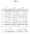
- Fig. 3 is a timing chart which shows an example of specific
operations of mainly a same line re-display read processing
circuit 114;
- Fig. 4 is a schematic block diagram of a conventional
liquid crystal display control apparatus as it handles a liquid
crystal display (image display) request and a host computer
access request;
- Fig. 5 is a schematic drawing which shows an example of
a 1-bit structure within a memory circuit and a relationship
with a line latch circuit;
- Fig. 6 is a timing chart which shows an example that there
is no contention between an access request from a host computer
and an access request for liquid crystal display (image
display); and
- Fig. 7 is a timing chart which shows an example that a
contention arises between an access request from a host computer
and an access request for liquid crystal display (image
display).
-
DETAILED DESCRIPTION OF PREFERRED EMBODIMENTS
-
An embodiment of the present invention will now be
described with reference to the associated drawings.
(Embodiment)
-
Fig. 1 is a drawing of a liquid crystal display control
apparatus according to an embodiment of the present invention
and a circuit which provides a method of controlling the liquid
crystal display apparatus.
-
In Fig. 1, denoted at 101 is a host computer.
-
Denoted at 102 is a host interface circuit. The host
interface circuit 102 transfers display data with the host
computer 101.
-
Denoted at 103 is a memory address counter circuit. The
memory address counter circuit 103 receives a write address from
the host interface circuit 102 and increments or decrements the
address. To be more specific, using the write address received
from the host interface circuit 102 as an initial value, the
memory address counter circuit 103 increases or decreases the
address. This structure is used for the following reason.
When the entire screen needs be rewritten or the screen needs
be rewritten only within a certain range (for instance, when
a moving picture is to be displayed partially within a still
image), automatic address update is executed after an initial
value has been set. Thus, a consideration is given to a fact
that increment/decrement, e.g., rotating of a liquid crystal
panel changes the top and the bottom or the right and the left
of the screen.
-
Denoted at 104 is a register setting circuit. The
register setting circuit 104 receives a register write address
and register write data from the host interface circuit 102.
-
Denoted at 105 is a display read clock signal generating
circuit. The display read clock signal generating circuit 105
generates a display read clock signal which serves as a
reference clock for displaying.
-
Denoted at 106 is a horizontal-direction counter circuit
for display. The horizontal-direction counter circuit for
display 106 counts the display read clock signal received from
the display read clock signal generating circuit 105. Although
not shown, the display read clock signal is fed not only to the
horizontal-direction counter circuit for display 106 but also
to other circuits which operate with reference to a display read
clock.
-
Denoted at 107 is a horizontal-counter decode circuit.
The horizontal-counter decode circuit 107 decodes an output
signal of the horizontal-direction counter circuit for display
106 and outputs a display read signal and a display line data
transfer signal. The display read signal is a signal for
initialization of a display read bus for the purpose of
displaying. Concurrently with this, data are transmitted
(transferred) to an input of a line latch circuit 121. The
display line data transfer signal causes a gate of the line latch
circuit 121 to open for data acquisition and to close, and data
is fixed after transmission of the display line data transfer
signal. It is on the occasion that the data is updated in
response to a host access during a period until transmission
of the display line data transfer signal since initialization
of the display read bus that display data is affected by an
address contention.
-
Denoted at 108 is a vertical-direction counter circuit
for display. The vertical-direction counter circuit for
display 108 receives a predetermined output value of the
horizontal-direction counter circuit for display 106 and
increments or decrements.
-
Denoted at 109 is a counter decode circuit. The counter
decode circuit 109 decodes an output from the
vertical-direction counter circuit for display 108 and an
output from the memory address counter circuit 103, and outputs
a memory write address and a display read address.
-
A description will now be given on a relationship between
a display read address and the outputs from the
vertical-direction counter circuit for display 108 which is
shown in Fig. 1 and a relationship between a memory write address
and the outputs from the memory address counter circuit 103
which is shown in Fig. 1. In a macro-operational sense, this
means the output from the vertical-direction counter circuit
for display 108 = the display read address. Despite this, the
timing of counting up is different in reality. The
vertical-direction counter circuit for display 108 updates a
count value when the count value of the horizontal-direction
counter circuit for display 106 is 0. After the
vertical-direction counter circuit for display 108 has updated
its count value, the display read address gets reflected
(counting operation) when the count value of the
horizontal-direction counter circuit for display 106 becomes
2. In the event that there is an access contention, once an
address coincidence detect signal 310 has been detected, the
display read address will not be updated even when the count
value of the horizontal-direction counter circuit for display
106 is 2.
-
This operation is included in operations of the counter
decode circuit 109, and the counter decode circuit 109 aligns
the widths of output bits so that an address coincidence detect
circuit 110 will detect coincidence.
-
The memory address counter circuit 103 outputs an
X-address and a Y-address of a memory area. The counter decode
circuit 109 is a block circuit which receives a counter output
corresponding to the Y-address of these and a counter output
corresponding to a display line address which is outputted from
the vertical-direction counter circuit for display 108. Since
the vertical-direction counter circuit for display 108 also
counts a blanking period, it is possible that an output bit count
of the memory address counter circuit 103 is different from that
of the vertical-direction counter circuit for display 108. The
counter decode circuit 109 is provided as the countermeasures
against this. It is also possible that the output bit counts
are not different.
-
To access the memory circuit 120, the memory address
counter circuit 103 generates an X-direction address and a
Y-direction address. A memory write address refers to an output
representing the Y-direction address as it has been aligned as
for bit count with the vertical-direction counter circuit for
display 108.
-
Denoted at 110 is the address coincidence detect circuit.
Receiving the memory write address and the display read address
outputted from the counter decode circuit 109, the address
coincidence detect circuit 110 judges whether the memory write
address coincides with the display read address.
-
Denoted at 111 is the access contention monitoring period
pulse generating circuit. The access contention monitoring
period pulse generating circuit 111 generates a pulse which
defines an access contention monitoring period based on an
output from the horizontal-counter decode circuit 107.
-
Denoted at 112 is an address contention judging circuit.
The address contention judging circuit 112 judges whether there
is a contention between the display read address and the memory
write address, based on outputs from the address coincidence
detect circuit 110 and the access contention monitoring period
pulse generating circuit 111.
-
Denoted at 113 is a host retry pulse generating circuit.
The host retry pulse generating circuit 113 receives a memory
write clock from the host interface circuit 102 and an output
from the address contention judging circuit 112, and during the
access contention monitoring period, generates a display read
signal and a display line data transfer signal based on the
memory write clock as an access contention arises.
-
Denoted at 114 is a same line re-display read processing
circuit. The same line re-display read processing circuit 114
receives a display read signal and a display line data transfer
signal outputted from the horizontal-counter decode circuit 107
and the output from the address contention judging circuit 112,
and during the access contention monitoring period, generates
a display read signal and a display line data transfer signal
which will be used for execution of the same line re-display
read processing, without moving to the next line as an access
contention arises.
-
Denoted at 115 is a normal read processing circuit. The
normal read processing circuit 115 generates a display read
signal and a display line data transfer signal which will be
used for execution of normal read processing, based on the
display read signal and the display line data transfer signal
outputted from the horizontal-counter decode circuit 107 and
an output value of the vertical-direction counter circuit for
display 108.
-
Denoted at 116 is a display read selection circuit. In
accordance with an output from the register setting circuit 104,
the display read selection circuit 116 selects a state that of
the display read signal outputted from the host retry pulse
generating circuit 113 and the display read signal outputted
from the same line re-display read processing circuit 114, only
the display read signal outputted from the host retry pulse
generating circuit 113 is outputted, a state that the display
read signal outputted from the same line re-display read
processing circuit 114 alone out of these two is outputted, or
a state that both the display read signal outputted from the
host retry pulse generating circuit 113 and the display read
signal outputted from the same line re-display read processing
circuit 114 are made valid and outputted.
-
Denoted at 117 is a line data transfer selection circuit.
In accordance with an output from the register setting circuit
104, the line data transfer selection circuit 117 selects a
state that of the display line data transfer signal outputted
from the host retry pulse generating circuit 113 and the display
line data transfer signal outputted from the same line
re-display read processing circuit 114, only the display line
data transfer signal outputted from the host retry pulse
generating circuit 113 is outputted, a state that the display
line data transfer signal outputted from the same line
re-display read processing circuit 114 alone out of these two
is outputted, or a state that both the line data transfer
selection circuit 117 selects a state that of the display line
data transfer signal outputted from the host retry pulse
generating circuit 113 and the display line data transfer signal
outputted from the same line re-display read processing circuit
114 are made valid and outputted.
-
Selecting operations of the display read selection
circuit 116 and the line data transfer selection circuit 117
mentioned above will now be described. To make the both signals
valid in the display read selection circuit 116 and the line
data transfer selection circuit 117 mentioned above means to
allow simultaneous execution of both a host retry (During
writing, post-writing data is always re-displayed.) and a
display retry (Without shifting the display line to the next
line, the same line is re-displayed.).
-
Since a display read signal and a display line data
transfer signal are generated as a pair in response to a host
retry, the both pulses are apart by a certain time difference.
When a host retry is executed in faster cycles than this time
difference, although the host retry operation does not become
valid, displaying of wrong data can be prevented since the
display retry operation becomes valid.
-
The selecting operations of the display read
selection
circuit 116 and the line data
transfer selection circuit 117
mentioned above may be combined for the following three
instances:
- a. When the host retry operation alone is desired;
- b. When the display retry operation alone is desired;
and
- c. When the host retry operation/the display retry
operation is desired (The both are made valid.).
-
-
Denoted at 118 is a retry display read selection circuit
which selectively outputs either one of the display read signal
outputted from the display read selection circuit 116 and the
display read signal outputted from the normal read processing
circuit 115 in accordance with an output from the register
setting circuit 104.
-
Denoted at 119 is a retry line data transfer selection
circuit which selectively outputs either one of the display line
data transfer signal outputted from the line data transfer
selection circuit 117 and the display line data transfer signal
outputted from the normal read processing circuit 115 in
accordance with an output from the register setting circuit 104.
-
Denoted at 120 is a memory circuit. The memory circuit
120 receives the output from the host interface circuit 102,
the output from the memory address counter circuit 103, the
output from the vertical-direction counter circuit for display
108, the output from the retry display read selection circuit
118 and the output from the retry line data transfer selection
circuit 119, and stores display data which are to be displayed
by the liquid crystal display apparatus.
-
In the memory circuit 120, denoted at NRE is a read enable
signal. Denoted at DOUT is a data output. Denoted at NCS is
a chip select signal. Denoted at DIN is a data input. Denoted
at NWE is a write enable signal. Denoted at XADR is a horizontal
address. Denoted at YADR is a vertical address. Denoted at
MCK is a memory write clock. Denoted at NLRD is a display line
read signal. Denoted at LADR is a line address.
-
Denoted at 121 is a line latch circuit. The line latch
circuit 121 receives the output from the memory circuit 120
(display read data output) and the output from the retry line
data transfer selection circuit 119 (display line data transfer
signal LD), and supplies an output to a drive circuit part of
the liquid crystal display apparatus.
-
Operations of this liquid crystal display control
apparatus will now be described.
-
A write access request from the host computer 101 is fed
to the host interface circuit 102. The address signal of thus
fed access request is supplied to the memory address counter
circuit 103. The memory address counter circuit 103 then
operates in response to the access request, thereby
sequentially updating a physical address value to the memory
circuit 120.
-
The host interface circuit 102 also outputs a register
write address and register write data and accordingly sets up
operation commands for the register setting circuit 104. The
display read selection circuit 116, the line data transfer
selection circuit 117, the retry display read selection circuit
118, the retry line data transfer selection circuit 119 and the
same line re-display read processing circuit 114 operate in
accordance with outputs from the register setting circuit 104,
namely, the operation commands thus set up.
-
Selecting operations of the selection circuits 116
through 119 mentioned above will now be described. As pulses
to be generated as a pair in response to a host retry, there
are two signals of a display read signal and a display line data
transfer signal. As signals needed for the display retry
operation, there also are two signals of a display read signal
and a display line data transfer signal. The selection circuits
116 through 119 above choose so that one of the two signals will
become valid, the both signals will become valid, or neither
a host retry nor a display retry will be exercised (= the
conventional operations).
-
The selecting operations are then fixed to the state which
has been set up at the beginning in the register setting circuit
104. Depending upon the settings, a combination such as the
normal read processing circuit 115 + the same line read
processing circuit 115 is selected.
-
The display read clock signal generating circuit 105
generates a display read clock signal which will be then fed
to the horizontal-direction counter circuit for display 106.
Every time the display read clock signal is fed, the
horizontal-direction counter circuit for display 106 updates
a counter value. An output from the horizontal-direction
counter circuit for display 106 is fed to the horizontal-counter
decode circuit 107 and the vertical-direction counter circuit
for display 108. The horizontal-counter decode circuit 107
decodes the output value of the horizontal-direction counter
circuit for display 106, and outputs a display read signal and
a display line data transfer signal. Meanwhile, the
vertical-direction counter circuit for display 108 counts up
or down every time the output value of the horizontal-direction
counter circuit for display 106 reaches a predetermined value.
-
An output from the vertical-direction counter circuit for
display 108 and an output from the memory address counter
circuit 103 are fed to the counter decode circuit 109, and a
display read address and a memory write address are each
outputted.
-
The outputs from the counter decode circuit 109 are fed
to the address coincidence detect circuit 110. The address
coincidence detect circuit 110 compares the display read
address with the memory write address, determines whether the
two addresses coincide with each other, and outputs the result.
-
The output from the horizontal-counter decode circuit 107
is fed to the access contention monitoring period pulse
generating circuit 111. An output from the access contention
monitoring period pulse generating circuit 111 and the output
from the address coincidence detect circuit 110 are fed to the
address contention judging circuit 112. The address
contention judging circuit 112 judges whether a contention has
occurred and outputs the result.
-
In response to the output from the address contention
judging circuit 112 and the output from the host interface
circuit 102, the memory write clock is fed to the host retry
pulse generating circuit 113. The host retry pulse generating
circuit 113 then generates a pair of a display read signal and
a display line data transfer signal from the memory clock, in
accordance with the result outputted from the address
contention judging circuit 112.
-
The output from the address contention judging circuit
112, the output from the horizontal-counter decode circuit 107
and the output from the register setting circuit 104 are fed
to the same line re-display read processing circuit 114. In
accordance with the result outputted from the address
contention judging circuit 112, that is, when an address
contention has occurred, the same line re-display read
processing circuit 114 then executes processing of
re-generating a display line data transfer signal for the
contention-bearing line.
-
Further, upon detection of the address contention, the
same line re-display read processing circuit 114 outputs a
horizontal-direction counter skip signal (307 in Fig. 3).
Receiving the horizontal-direction counter skip signal (307 in
Fig. 3), the horizontal-direction counter circuit for display
106 skips a horizontal-direction counter value to (N-1).
-
The output from the horizontal-counter decode circuit 107
and the output from the vertical-direction counter circuit for
display 108 are fed to the normal read processing circuit 115.
The normal read processing circuit 115 executes the normal read
processing. As a result, the liquid crystal display apparatus
displays the display data as an image.
-
The output from the host retry pulse generating circuit
113 and the output from the same line re-display read processing
circuit 114 are supplied to the display read selection circuit
116, and an output of the display read selection circuit 116
is determined in accordance with the output from the register
setting circuit 104. To be specific, a state that of a display
read signal outputted from the host retry pulse generating
circuit 113 and a display read signal outputted from the same
line re-display read processing circuit 114, only the display
read signal outputted from the host retry pulse generating
circuit 113 is outputted, a state that the display read signal
outputted from the same line re-display read processing circuit
114 alone out of these two is outputted, or a state that both
the display read signal outputted from the host retry pulse
generating circuit 113 and the display read signal outputted
from the same line re-display read processing circuit 114 are
made valid and outputted is selected, in accordance with the
output from the register setting circuit 104.
-
The output from the display read selection circuit 116
and the output from the normal read processing circuit 115 are
supplied to the retry display read selection circuit 118, and
an output of the retry display read selection circuit 118 is
determined in accordance with the output from the register
setting circuit 104. To be specific, either the display read
signal outputted from the display read selection circuit 116
or the display read signal outputted from the normal read
processing circuit 115 is selectively outputted in accordance
with the output from the register setting circuit 104.
-
In a similar fashion, the output from the host retry pulse
generating circuit 113 and the output from the same line
re-display read processing circuit 114 are supplied to the line
data transfer selection circuit 117, and an output of the line
data transfer selection circuit 117 is determined in accordance
with the output from the register setting circuit 104. To be
specific, a state that of a display line data transfer signal
outputted from the host retry pulse generating circuit 113 and
a display line data transfer signal outputted from the same line
re-display read processing circuit 114, only the display line
data transfer signal outputted from the host retry pulse
generating circuit 113 is outputted, a state that the display
line data transfer signal outputted from the same line
re-display read processing circuit 114 alone of these two is
outputted, or a state that both the display line data transfer
signal outputted from the host retry pulse generating circuit
113 and the display line data transfer signal outputted from
the same line re-display read processing circuit 114 are made
valid and outputted is selected, in accordance with the output
from the register setting circuit 104.
-
The output from the line data transfer selection circuit
117 and the output from the normal read processing circuit 115
are supplied to the retry line data transfer selection circuit
119, and an output of the retry line data transfer selection
circuit 119 is determined in accordance with the output from
the register setting circuit 104. To be specific, either the
display line data transfer signal outputted from the line data
transfer selection circuit 117 or the display line data transfer
signal outputted from the normal read processing circuit 115
is selectively outputted in accordance with the output from the
register setting circuit 104.
-
This makes it possible to select whether to always update
display data to the latest state during writing upon occurrence
of an access contention. Further, it is possible to select
whether to execute the same line re-display read processing when
an access contention has occurred.
-
When there is no access contention, the normal read
processing is carried out.
-
In the case of a host retry, whether to output a pair of
pulses and the normal read processing circuit may be selected.
-
Meanwhile, for a display retry, it is necessary that the
content of the processing is switched appropriately for when
there is an access contention and for when there is no access
contention. In Fig. 1, the register selects such that the
normal read processing circuit 115 and the same line re-display
read processing circuit 114 will have OR-like structures. As
an access contention arises, the same line re-display read
processing circuit 114 receives the signal from the address
contention judging circuit 112, and upon receipt of the signal,
a processing signal which invalidates the signal from the normal
read processing circuit 115 is outputted also from the same line
re-display read processing circuit 114. To be specific, the
address coincidence detect signal 310 shown in Fig. 3 is
outputted also from the same line re-display read processing
circuit 114, thereby invalidating pulses like a display line
data transfer signal 311.
-
Although the selection circuits 116 through 119 above are
referred to as selection circuits, the selection circuits are
selectively combined with each other instead of choosing only
one of the selection circuits.
-
Further, in accordance with a combination of the outputs
from the register setting circuit 104, it is possible to allow
only the output from the retry display read selection circuit
118, only the output from the retry line data transfer selection
circuit 119, or the outputs from both the retry display read
selection circuit 118 and the retry line data transfer selection
circuit 119, and hence, to avoid displaying of display data
which has been influenced by an access contention.
-
The selecting operations of the selection circuits 116
through 119 above will now be further described. Since a
display read signal and a display line data transfer signal are
generated in a pair for a host retry, there is a certain time
difference between pulses. When a host access is made in cycles
which are faster than this time difference, the host retry
operation does not become valid. In such a case, the display
retry operation is selected, whereby displaying of wrong data
is prevented. Conversely, since execution of a display retry
extends the duration of the retried line when a host access is
in slow cycles, the frame frequency for displaying of an image
could decrease and the displaying quality could deteriorate,
and therefore, selection of the host retry operation can prevent
displaying of wrong data in such a case. Outputting of the both
may be chosen when it is hard to determine the host access cycles,
to thereby benefit from the both effects and prevent displaying
of wrong data.
-
At the time of the retry operation, the output from the
normal read processing circuit is always handled as if the
output was OR. Even when only a host retry is chosen, they must
execute the normal read processing in the absence of a host
access. Even when only a display retry is chosen, they must
execute the normal read processing unless an access contention
arises.
-
Even though the output is handled as if it was OR, upon
occurrence of an access contention, they receive from the host
retry pulse generating circuit 113, the same line re-display
read processing circuit 114 or the like something resembling
an enable signal which invalidates the normal read processing
and prioritizes processing of a host retry or processing of a
display retry, whereby invalidating processing is performed.
-
The register settings may realize the following three
selections:
- 1. Where whether to execute the host retry processing
is to be selected, when the host retry processing is to be
executed, the host retry processing + the normal read processing
circuit is selected;
- 2. Where whether to execute the display retry
processing is to be selected, when the display retry processing
is to be executed, the display retry processing + the normal
read processing circuit is selected; and
- 3. Where no retry processing is to be executed for 1.
or 2., the normal read processing circuit is selected.
-
-
The memory circuit 120 receives the outputs of the host
interface circuit 102 (the chip select signal, write data, the
memory write clock), the output of the retry display read
selection circuit 118 (the display read signal), the output of
the retry line data transfer selection circuit 119 (the display
line data transfer signal) and the output of the
vertical-direction counter circuit for display 108 (line
address), whereby display data is stored. The line latch
circuit 121 receives thus stored display data line by line as
the output from the memory circuit 120 in accordance with the
output from the retry line data transfer selection circuit 119
(the display line data transfer signal). The output from the
line latch circuit 121 is propagated to an LCD drive circuit
part.
-
Operations of the host retry pulse generating circuit 113
and the same line re-display read processing circuit 114 will
now be described.
-
Fig. 2 is a timing chart of a specific example of mainly
the host retry pulse generating circuit 113.
-
In Fig. 2, denoted at 201 is the display read clock signal
outputted from the display read clock signal generating circuit
105. Denoted at 202 is the horizontal-direction counter signal
outputted from the horizontal-direction counter circuit for
display 106. Denoted at 203 is the display read signal
outputted from the normal read processing circuit 115. Denoted
at 204 is the display line data transfer signal outputted from
the normal read processing circuit 115. Denoted at 205 is the
display read address signal outputted from the counter decode
circuit 109. Denoted at 206 is an access contention monitoring
period pulse signal outputted from the access contention
monitoring period pulse generating circuit 111. Denoted at 207
is the memory write address signal outputted from the counter
decode circuit 109. Denoted at 208 is the address coincidence
detect signal outputted from the address coincidence detect
circuit 110. Denoted at 209 is the memory write clock signal
outputted from the host interface circuit 102. Denoted at 210
is the display read signal outputted from the host retry pulse
generating circuit 113. Denoted at 211 is the display line data
transfer signal outputted from the host retry pulse generating
circuit 113.
-
The retry operations associated with the host retry pulse
generating circuit 113 will now be described. The
horizontal-direction counter signal 202 is counted up
sequentially in response to the display read clock signal 201
and returns to zero as the counter value reaches a predetermined
value N. The display read signal 203 shows a high-level pulse
when the value of the horizontal-direction counter signal 202
becomes N. The display line data transfer signal 204 shows a
high-level pulse when the value of the display read clock signal
201 becomes 1.
-
The access contention monitoring period pulse 206 is a
signal which defines the duration from the timing T201 at which
the display read signal 203 rises to the timing T202 at which
the display line data transfer signal 204 falls, and therefore,
indicates that this duration is a period which is influenced
by an address contention. The address coincidence detect
signal 208 which is at the high level is generated when the memory
write address signal 207 becomes to represent an address M while
the display read address signal 205 is indicative of the address
M and the access contention monitoring period pulse 206 is
active, that is, during a period from the timing T203 to the
timing T204. As the address coincidence detect signal 208 is
generated, the host retry pulse generating circuit 113
generates the display read signal 210 and the display line data
transfer signal 211 in synchronization to the memory write clock
signal 209.
-
Once the display read signal 210 and the display line data
transfer signal 211 have been thus generated as a pair, every
time an access contention arises at the timing T207, the line
latch circuit 121 is updated to the latest information. This
prevents displaying of wrong data. As a pulse pair T208 (i.e.,
the display read signal 210 and the display line data transfer
signal 211) is generated at the timing T203 which is the start
of the access contention monitoring period, in the absence of
an access contention, processing equivalent to the normal
display read is executed except for that no updating is
performed.
-
When a host retry is desired, as the access contention
monitoring period starts, the display read signal and the
display line data transfer signal are outputted as a pair first,
and the display read data is then updated. This is because the
access contention monitoring period has already started (i.e.,
the normal display read signal has been already received). It
is important to update the display data immediately after the
start of the access contention monitoring period regardless of
whether there is an access contention. For instance, unlike
in Fig. 2, if no access contention occurs after this, owing to
the updating of the display data executed at the beginning, the
data on this display line will be read (which is the same as
refreshing). But for these first signals, no pulse will be
generated in the absence of a contention. This means that no
line data transfer signal will be outputted, the line count
corresponding to the display line alone will be updated, and
the line data information on the immediately precedent line will
be displayed continuously as the display data. To prevent this,
immediately after the start of the access contention monitoring
period, pulses are generated once regardless of whether a
contention has occurred.
-
In Fig. 2, as the host retry is to be executed, the output
from the same line re-display read processing circuit 114 is
invalidated. Hence, the signals from the host retry pulse
generating circuit 113 and the normal read processing circuit
become valid. However, the output from the normal read
processing circuit 115 in the host retry mode is utilized for
generation of the access contention monitoring period pulse.
-
Fig. 3 is a timing chart which shows an example of specific
operations of mainly the same line re-display read processing
circuit 114.
-
In Fig. 3, denoted at 301 is the display read clock signal
outputted from the display read clock signal generating circuit
105. Denoted at 302 is the horizontal-direction counter signal
outputted from the horizontal-direction counter circuit for
display 106. Denoted at 303 is the display read signal
outputted from the normal read processing circuit 115. Denoted
at 304 is the display line data transfer signal outputted from
the normal read processing circuit 115. Denoted at 305 is the
display read address signal outputted from the counter decode
circuit 109. Denoted at 306 is an access contention monitoring
period pulse signal outputted from the access contention
monitoring period pulse generating circuit 111. Denoted at 307
is the horizontal-direction counter skip signal. Denoted at
308 is the vertical-direction counter signal outputted from the
vertical-direction counter circuit for display 108. Denoted
at 309 is the memory write address signal outputted from the
counter decode circuit 109. Denoted at 310 is the address
coincidence detect signal outputted from the address
coincidence detect circuit 110. Denoted at 311 is the line data
transfer signal outputted from the same line re-display read
processing circuit 114. Denoted at 312 is an address state
during display read by the same line re-display read processing
circuit 114. Denoted at T301 is a display line period upon
occurrence of an access contention. Denoted at T302 is the same
line re-display read line period. Denoted at T303 is the next
read line period.
-
The horizontal-direction counter signal 302 is
sequentially updated in response to the display read clock
signal 301 and returns to zero as the counter value reaches the
predetermined value N. The display read signal 303 shows a
high-level pulse when the value of the horizontal-direction
counter signal 302 becomes N. The display line data transfer
signal 304 shows a high-level pulse when the value of the
horizontal-direction counter signal 302 becomes 1. The access
contention monitoring period pulse signal 306 is a signal which
defines the duration from rising of the display read signal 301
to falling of the display line data transfer signal 304, and
this duration is a period which is influenced by an address
contention. The address coincidence detect signal 310 which
is at the high level is generated when the value of the memory
write address signal 309 reaches M while the value of the display
read address 305 is M and during the period T304 that the access
contention monitoring period pulse signal 306 remains valid.
-
As the address coincidence detect signal 310 is generated,
the same line re-display read processing circuit 114 executes
such processing that a high-level pulse of the line data
transfer signal 311 will not be generated during T306. Since
the line data transfer signal 311 is not generated at the timing
T306 while the vertical-direction counter signal 308 is updated
to M + 1, the line data will not be transferred. Since the
display read address 305 does not refer to the value of the
vertical-direction counter signal 308, even after the value of
the vertical-direction counter signal 308the display data on
the M line has been updated to (M + 1) because of the
vertical-direction counter signal 308, the display read address
305 remains M, and the display data on the M line displayed again,
the same line is displayed again (T301, T302).
-
Once the address coincidence detect signal 310 has been
generated, the horizontal-direction counter skip signal 307 is
generated at the timing T305 and the horizontal-direction
counter signal 302 is skipped to N - 1. During the same line
re-display read line period T302, the value of the
horizontal-direction counter signal 302 is skipped to (N - 1)
in accordance with the horizontal-direction counter skip signal
307 and the value of the vertical-direction counter signal 308
is returned to M which is the immediately precedent value. When
the value of the horizontal-direction counter signal 302
returns to zero later, the vertical-direction counter signal
308 is updated and remains as (M + 1).
-
Further describing this, the vertical-direction counter
value does not directly represent a display line. A display
line has the value of the display read address 305. As
operations inside the circuit, the count is updated with the
end-most count value of the horizontal-direction counter signal
302 with reference to the vertical-direction counter signal 308.
However, at this point, the display line has the value of the
display read address 305. In short, while the display read
address 305 is updated with reference to the value of the
vertical-direction counter signal 308 when there is no access
contention, upon occurrence of an access contention, the value
of the vertical-direction counter signal 308 is not referred
to and the display line is not updated.
-
Changes of the display read address 305, the
vertical-direction counter 308, the line data transfer signal
311 and the display data 312 will now be described in detail.
The vertical-direction counter 308 updates the count value when
the count value of the horizontal-direction counter 302 becomes
zero. With reference to this count value, the display read
address 305 updates the count value as the count value of the
horizontal-direction counter 302 becomes 2 (i.e., when the
display line data transfer signal 304 falls). However, the
display read address 305 does not update the count value if the
address coincidence detect signal 310 is high. Further, when
the address coincidence detect signal 310 is high, the line data
transfer signal 311 masks the display line data transfer signal
304. Thus, the line data transfer signal 311 does not turn on
during the period denoted at the symbol o, and therefore, the
data in the line latch circuit 121 fails to be re-written and
the display data remains as the non-updated data which is at
the M line. In short, when the display line data transfer signal
629 does not turn on as described with reference to the operation
chart in Fig. 7, the previous data remains outputted as the
output from the line latch circuit. The display data 312
therefore becomes as shown in Fig. 3.
-
Fig. 3 is for description of the same line re-display read
processing for contending operations, and the values of the
display read address 305 and the vertical-direction counter 308
do not change in association with each other. This will now
be described in detail.
-
The display read address 305 is the address of the
currently displayed line. The display read address 305 is
counted (UP/DOWN) at the timing of the next display read clock
301 (= when the horizontal-direction counter value becomes 2)
after outputting of the display line data transfer signal 304,
during the normal operations. In contrast, the
vertical-direction counter signal 308 is counted (UP/DOWN)
usually when the value of the horizontal-direction counter
signal 302 is zero. In response to outputting of the display
line data transfer signal 304, the display read address 305
becomes indicative of the value of the vertical-direction
counter signal 308 in synchronization to the next display read
clock 301. The display line data transfer signal 304 in Fig.
3 represents the output timing during the normal operations,
while the line data transfer signal 311 represents the output
timing upon occurrence of a contention, during the re-display
read processing and at the normal time. The display read
address 305 is indicative of a contention-induced decode value
which corresponds to outputting of the address coincidence
detect signal 310.
-
Although updating to (M + 1) is supposed to take place
since the vertical-direction counter signal 308 has become (M
+ 1), M is kept without any updating to (M + 1) since the line
data transfer signal 311 has not turned on. Because of this,
the display line will not move to the next line, and in an effort
to execute the re-display read processing on the same line, the
horizontal-direction counter skip signal 307 will turn on and
the horizontal-direction counter value will skip to N - 1 for
displaying again. When no address contention has not occurred
yet at the time of the re-display operation, the pulse T307 of
the line data transfer signal 311 appears and the normal
operations are restored. In the event that a contention has
occurred, the skip operation is repeated during the period T302.
-
In the host retry mode, the output of the normal read
processing circuit 115 is utilized for generation of the access
contention monitoring period pulse but is not used as a display
read signal or display line data transfer signal for the purpose
of displaying. A display read signal and a display line data
transfer signal generated as a pair are used in the host retry
mode. Paired pulses are generated at the beginning of the
access contention monitoring period in the host retry mode and
this pair plays the role of the normal read processing, and
therefore, the output from the normal read processing circuit
115 is not necessary.
-
In the display retry mode, the output of the normal read
processing circuit 115 is used. Upon occurrence of a contention,
the same line re-display read processing circuit 114 outputs
the mask signal and the display line data transfer signal from
the normal read processing circuit 115 is made invalid. When
the host retry mode and the display retry mode are both to be
active, the paired pulses generated at the beginning of the
access contention monitoring period for the host retry mode
function as pulses which are demanded for each line for the
normal read processing. Hence, even though a display retry has
not been attempted, the same processing as the normal read
processing is executed. When there is an attempted display
retry, although the processing of masking the display line data
transfer signal is performed, since the signals for the normal
read processing are unusable owing to the register settings
corresponding to the activation of the both modes, the
re-display read processing alone is performed except for
masking of the display line data transfer signal.
-
A difference between the address coincidence detect
signals 208 and 310 shown in Figs. 2 and 3 will now be described.
-
Fig. 3 is for describing the display retry mode. In the
display retry mode, as an access contention arises during the
access contention monitoring period (= from rising of the
display read signal 303 to falling of the display line data
transfer signal 304; the access contention monitoring period
pulse signal 306), the re-display read processing is performed
on the same line after the access contention monitoring period
has ended. Since the processing is thus executed in response
even to one access contention during the access contention
monitoring period, however more often contentions arise during
the access contention monitoring period, outputting of the
detect signal responding to the first contention would be enough.
By means of latching of the first contention detect signal, the
pulse width of the address coincidence detect signal 310 widens.
-
Fig. 2 is for describing the host retry mode. In the host
retry mode, every time an access contention arises owing to a
write access made by the host computer during the access
contention monitoring period (= from rising of the display read
signal 203 to falling of the display line data transfer signal
204; the access contention monitoring period pulse signal 206),
re-display read of the latest data written within the cycles
is performed. To this end, a display read signal and a display
line data transfer signal are generated as a pair. Once the
pair of the display read signal and the display line data
transfer signal has been thus generated, the address
coincidence detect signal is turned off and the next access
contention is monitored. The address coincidence detect
signal therefore falls at the location where the display line
data transfer signal 211 falls.
-
A display read signal and a display line data transfer
signal to be fed to the memory circuit are summarized as shown
in the table below.
| Mode | Host retry | Display retry | Normal read |
| | Display read signal | Line data transfer signal | Display read signal | Line data transfer signal | Display read signal | Line data transfer signal |
| Host retry | | ○ | × | × | × | × |
| Display retry | | × | O | O | O | O |
| Host retry + display retry | O | O | × | O | × | × |
| Normal processing | × | × | × | × | O | O |
-
In the table above, the pulses for the normal processing
are invalidated during the display retry processing, upon
occurrence of a contention.
-
This is repeated until the address coincidence detect
signal 310 becomes undetected or for a predetermined number of
times. With the horizontal-direction counter signal 302
skipped, it is possible on the display read side to forcedly
shift the phase in which an access contention arises and
accordingly prevent displaying of wrong data. As the address
coincidence detect signal 310 becomes turned off, the display
line data transfer signal in the same line re-display read
processing circuit 114 is generated as shown at the timing T307,
the period proceeds to the next line period T302, and the
vertical-direction counter signal 308 resumes updating. The
display read signal 303 is always outputted at the illustrated
timing regardless of whether a contention has occurred. When
a display retry is attempted, the signal is masked like the
display line data transfer signal 311 as a contention occurs,
but is outputted normally when no contention has occurred.
-
The polarities of the signals, the counter values and the
like shown in Figs. 2, 3, 4, 5 and 6 are mere examples.
-
Although both the host retry pulse generating circuit 113
and the same line re-display read processing circuit 114 are
disposed and these are selectively used by means of the display
read selection circuit 116 and the line data transfer selection
circuit 117 or the both are made valid and used according to
the embodiment described above, it is not necessary to dispose
both the host retry pulse generating circuit 113 and the same
line re-display read processing circuit 114. Either one of
these may be disposed instead. In that case, neither the
display read selection circuit 116 nor the line data transfer
selection circuit 117 is needed of course.
-
In addition, while the embodiment described above is
directed to an example that the image display control method
and the image display control apparatus of the present invention
are applied to a liquid crystal display control apparatus, the
present invention is not limited only to a liquid crystal
display control apparatus but is similarly applicable to a
plasma display control apparatus and an EL
(electro-luminescence) display control apparatus which have a
structure that data covering one line is read for displaying
in accordance with a read signal.
-
When a contention is detected between a memory write
address and a display read address in a memory circuit which
stores display data, a host retry pulse generating circuit
generates a display read signal and a display line data transfer
signal based on a memory write clock, and supplies these to the
memory circuit while supplying the display line data transfer
signal to a line latch circuit. Alternatively, upon detection
of the contention above, a same line re-display read processing
circuit performs same line re-display read processing without
moving to the next line, and supplies a display read signal and
a display line data transfer signal to the memory circuit while
supplying the display line data transfer signal to the line
latch circuit.