EP1475651A1 - Waveguide type optical module, and temperature control component, and temperature control element thereof - Google Patents
Waveguide type optical module, and temperature control component, and temperature control element thereof Download PDFInfo
- Publication number
- EP1475651A1 EP1475651A1 EP03701735A EP03701735A EP1475651A1 EP 1475651 A1 EP1475651 A1 EP 1475651A1 EP 03701735 A EP03701735 A EP 03701735A EP 03701735 A EP03701735 A EP 03701735A EP 1475651 A1 EP1475651 A1 EP 1475651A1
- Authority
- EP
- European Patent Office
- Prior art keywords
- plate
- pedestal
- contact
- optical module
- control element
- Prior art date
- Legal status (The legal status is an assumption and is not a legal conclusion. Google has not performed a legal analysis and makes no representation as to the accuracy of the status listed.)
- Withdrawn
Links
Images



Classifications
-
- G—PHYSICS
- G02—OPTICS
- G02B—OPTICAL ELEMENTS, SYSTEMS OR APPARATUS
- G02B6/00—Light guides; Structural details of arrangements comprising light guides and other optical elements, e.g. couplings
- G02B6/24—Coupling light guides
- G02B6/42—Coupling light guides with opto-electronic elements
- G02B6/4201—Packages, e.g. shape, construction, internal or external details
-
- G—PHYSICS
- G02—OPTICS
- G02B—OPTICAL ELEMENTS, SYSTEMS OR APPARATUS
- G02B6/00—Light guides; Structural details of arrangements comprising light guides and other optical elements, e.g. couplings
- G02B6/10—Light guides; Structural details of arrangements comprising light guides and other optical elements, e.g. couplings of the optical waveguide type
- G02B6/12—Light guides; Structural details of arrangements comprising light guides and other optical elements, e.g. couplings of the optical waveguide type of the integrated circuit kind
- G02B6/12007—Light guides; Structural details of arrangements comprising light guides and other optical elements, e.g. couplings of the optical waveguide type of the integrated circuit kind forming wavelength selective elements, e.g. multiplexer, demultiplexer
-
- G—PHYSICS
- G02—OPTICS
- G02B—OPTICAL ELEMENTS, SYSTEMS OR APPARATUS
- G02B6/00—Light guides; Structural details of arrangements comprising light guides and other optical elements, e.g. couplings
- G02B6/24—Coupling light guides
- G02B6/42—Coupling light guides with opto-electronic elements
- G02B6/4201—Packages, e.g. shape, construction, internal or external details
- G02B6/4266—Thermal aspects, temperature control or temperature monitoring
- G02B6/4268—Cooling
- G02B6/4271—Cooling with thermo electric cooling
-
- G—PHYSICS
- G02—OPTICS
- G02B—OPTICAL ELEMENTS, SYSTEMS OR APPARATUS
- G02B6/00—Light guides; Structural details of arrangements comprising light guides and other optical elements, e.g. couplings
- G02B6/10—Light guides; Structural details of arrangements comprising light guides and other optical elements, e.g. couplings of the optical waveguide type
- G02B6/12—Light guides; Structural details of arrangements comprising light guides and other optical elements, e.g. couplings of the optical waveguide type of the integrated circuit kind
- G02B2006/12133—Functions
- G02B2006/12135—Temperature control
-
- G—PHYSICS
- G02—OPTICS
- G02B—OPTICAL ELEMENTS, SYSTEMS OR APPARATUS
- G02B6/00—Light guides; Structural details of arrangements comprising light guides and other optical elements, e.g. couplings
- G02B6/24—Coupling light guides
- G02B6/26—Optical coupling means
- G02B6/30—Optical coupling means for use between fibre and thin-film device
-
- G—PHYSICS
- G02—OPTICS
- G02F—OPTICAL DEVICES OR ARRANGEMENTS FOR THE CONTROL OF LIGHT BY MODIFICATION OF THE OPTICAL PROPERTIES OF THE MEDIA OF THE ELEMENTS INVOLVED THEREIN; NON-LINEAR OPTICS; FREQUENCY-CHANGING OF LIGHT; OPTICAL LOGIC ELEMENTS; OPTICAL ANALOGUE/DIGITAL CONVERTERS
- G02F2203/00—Function characteristic
- G02F2203/21—Thermal instability, i.e. DC drift, of an optical modulator; Arrangements or methods for the reduction thereof
Definitions
- the present invention relates to a waveguide type optical module, a temperature controller and temperature control element for controlling the temperature of an optical waveguide having a temperature-dependent wavelength demultiplexing characteristic.
- the conventional waveguide type optical module especially, the quartz-array waveguide type optical module with an optical wavelength multi/demultiplexing function, uses a waveguide having a temperature-dependent wavelength demultiplexing characteristic.
- the waveguide type optical module of this type needs a temperature control of the waveguide for maintaining a required wavelength demultiplexing characteristic.
- an optical modulator or an optical switch whose refractive index is adjusted by changing the temperature for the optical deflection, should have the temperature thereof adjusted for the refractive index not to vary. Both of these requires a temperature controller for adjusting the temperature of the optical waveguide.
- Such a temperature controller is known from the disclosure in JP-A-2001-116936.
- the disclosed temperature controller is used in a quartz-array waveguide type optical module in which a heater is provided on a plate, which appears as a ceramic substrate, whose thermal expansion coefficient is 5 ppm/°C or less and thermal conductivity is 100 W/m ⁇ K or more, the plate is held on a pedestal and an optical waveguide is formed on the plate.
- the conventional waveguide type optical module is designed only for providing a temperature controller made of a material having a small thermal expansion coefficient and a good thermal conductivity. Therefore, the temperature distribution is not homogeneous over the surface of the plate as the temperature control element. Thus, the waveguide inevitably incurs a distortion and has the wavelength demultiplexing characteristic thereof degraded.
- the waveguide fixed on the plate has to be heated up to a predetermined temperature in a short time and held at the temperature.
- heat is not efficiently conducted from the plate heated by a heater to the waveguide, so it is not possible to elevate the temperature of the waveguide to higher than a certain point.
- heat generated by the heater is conducted partially to the plate and also to the waveguide.
- the heat conducted to the plate will be dissipated to the external space via the pedestal. Therefore, even if the heater is designed to have an increased area and it is supplied with an increased amount of electric power, the heat generated by the heater will not effectively be conducted to the waveguide. So, the waveguide cannot be heated up to higher than a certain point.
- a wavelength which should be demultiplexed is not demultiplexed to a core as a desired waveguide or causes optical signals to fail in functioning.
- the present invention has a primary object to overcome the above-mentioned drawbacks of the related art by providing a waveguide type optical module suitable for a design having multiple optical waveguides and excellent in wavelength demultiplexing characteristic.
- the present invention has another object to provide a temperature controller and temperature control element for use in the waveguide type optical module, incurring less occurrence of a particle count and showing a highly homogeneous distribution of temperature over the plate surface.
- the Inventors of the present invention made many experiments and researches and found that when the area of contact between the pedestal and plate was too large (32% or more), the temperature distribution was not homogeneous over the plate of the temperature control element and the temperature of the waveguide was not elevated to higher than a certain point. Also, the Inventors found that by reducing the contact area , the above drawbacks could be overcome and hence a waveguide type optical module could be provided which is excellent in wavelength demultiplexing characteristic.
- a waveguide type optical module including a temperature control element supported on pedestal inside a casing, and an optical waveguide disposed in contact on the temperature control element, wherein:
- a temperature controller for use in a waveguide type optical module, the temperature controller including a temperature control element held inside a casing and which includes a plate having a heater or heat absorber provided on a non-heating side thereof or buried therein; and there is installed to the plate a pedestal for supporting the plate thereon so that the area of contact with the pedestal and the non-heating side of the plate is less than 30% of the surface area of the plate.
- a temperature control element includes a plate having a heater or heat absorber provided on a non-heating side thereof or buried therein, wherein the plate is shaped so that the area of contact with a pedestal which support the plate thereon is less than 30% of the surface area of the plate.
- each pedestal should preferably be a one which is put into contact with the edge of the plate to support the latter. Further, the pedestal should more preferably be a one which is put into contact with the end face of the plate to support the latter.
- the plate should preferably be a ceramic-made one.
- a waveguide type optical module including a temperature control element supported on a pedestal inside a casing, and an optical waveguide disposed in contact on the temperature control element, wherein:
- ⁇ 2 should preferably be 5 to 40 % of ⁇ 1, the total area of the pedestal preferably be within a range of 1 to 25 % of the surface area of the plate, and the area of each pedestal preferably be within a range of 0.4 to 7 % of the surface area of the plate.
- the temperature control element includes the plate having the heater or heat absorber on the non-heating side thereof, or buried in, so the temperature of the plate can be increased and decreased relatively uniformly over the plate surface.
- the heater or heat absorber is provided on the non-heating side (rear side) of the plate, the heating can be made more homogeneously since heat will be conducted while being dispersed over the plate surface when it is propagated to a heating side of the plate. That is, since the plate functions to disperse the heat, it is possible to prevent the heat from being distributed inhomogeneously due to a wiring patter of the heater of heat absorber.
- the plate since inside the casing, the plate is supported in air being isolated by the pedestal from the bottom of the casing, so an air layer exists between the plate itself and casing bottom, which provides an effect of heat insulation.
- the plate is thermally insulated more effectively and homogeneous temperature distribution on the heating side can be assured and temperature elevation can be done at a higher rate.
- the area of contact between the pedestal and rear side of the plate is less than about 30% of the rear surface area of the plate, which is also intended for prevention of a cooling spot from being defined on the plate. If the area of contact between the pedestal and plate rear side exceeds 30% of the area surface area of the plate, the pedestal becomes a conductor of heat to the casing and thus the heat is dissipated to outside from the casing.
- the area of contact between the pedestal and plate rear side should preferably be 0.5 to 25 % of the rear surface area of the plate because the plate made of ceramic, if applied, can incur less occurrence of a particle count as the contact area is thus decreased. It should be noted that it is necessary to reduce the particles adhering, if occur, to the end face of the waveguide and causing a propagation loss.
- the plate should preferably be shaped to be generally rectangular and be supported on the pedestal in contact with each outer comer thereof.
- ⁇ 2 should preferably be 5 to 40 % of ⁇ 1, the total area of the pedestal preferably be within a range of 1 to 25 % of the surface area of the plate, and the area of each pedestal preferably be within a range of 0.4 to 6 % of the surface area of the plate.
- the pedestal is provided between the temperature control element and casing to isolate the latter, and the area of contact between the pedestal and plate is limited to as minimum as possible, thereby assuring a homogeneous temperature distribution over the surface of the plate as a temperature control element (heater plate) and a reduced time for heat elevation.
- the contact between the pedestal and plate may be an indirect contact using an adhesive or the like alternatively of the aforementioned one.
- the pedestal should preferably support the plate in contact with the edge (outer edge) of the latter, and more preferably support the plate in contact with each outer comer of the latter.
- the plate may be supported on the pedestal with the end face thereof placed on the pedestal.
- the end face of the plate are exposed to the fluidic atmosphere such as air, so heat is easily dissipated from there and thus they will have the temperature thereof easily lowered.
- the plate With the plate being placed in contact at the end face thereof with on the pedestal, it is possible to prevent the edge of the plate from being exposed to a highly fluidic atmosphere and thus effectively prevent the temperature at the plate edge from being lower.
- FIG. 2 is a sectional view of the pedestal
- FIGS. 3 and 4 are sectional side elevation and sectional front view, respectively, of the temperature controller shown in FIG 1.
- the temperature control element for use in the waveguide type optical module typically includes a plate 2 and a heater 3 disposed on a side (rear side) opposite to a heating side of the plate 2 on which a waveguide is disposed.
- a Peltier element as a heat absorber may be provided in place of the heater 3.
- the Peltier element has the functions of both the heater and heat absorber.
- pads 4 On the area (inner) of the plate 2 where the heater 3 is formed, there are provided pads 4 on which a thermistor chip and platinum resistance chip, used for measurement of a temperature, are mounted, heater power lead wires 7 for electrical connection with the pads 4, and thermistor lead wires 8.
- a thermistor chip and platinum resistance chip are mounted on the pads 4 to measure a temperature for the purpose of temperature control.
- the plate 2 may be formed from a metal plate, ceramic plate, resin plate, or the like.
- the metal plate include an aluminum plate, copper plate and the like.
- the ceramic plate may include more than one selected from among a nitride ceramics, carbide ceramics, oxide ceramics and carbon. For example, since the nitride ceramics and carbide ceramics are smaller in thermal expansion coefficient than the metal and considerably greater in mechanical strength than the metal, a thin ceramic plate will not be warped or distorted even when heated. Therefore, the plate 2 can be formed from a thin and lightweight ceramic plate.
- such a ceramic plate is characterized in that the surface temperature thereof will quickly respond to a change in temperature of a resistance heater because of the high heat conductivity and small thickness of the ceramic plate.
- the ceramic plate can advantageously have the surface temperature thereof controlled when changing the temperature of the resistance heater by changing the voltage or current supplied to the heater.
- the nitride ceramics may be aluminum nitride, silicon nitride, boron nitride, titanium nitride or the like, for example, and they may be used singly or more than two of them be used in combination.
- the carbide ceramics may be silicon carbide, boron carbide, titanium carbide, tantalum carbide, tungsten carbide or the like, for example and they may be used singly or more than two of them be used in combination.
- the aluminum nitride is most preferable for forming the plate 2 because it has a highest heat conductivity as 180 W/m.K and it is outstanding in temperature response.
- the ceramic used as a material for the plate 2 shows a small thermal expansion coefficient and has only a small difference in thermal expansion from a waveguide 12 even when the temperature becomes high, the waveguide 12 will not be broken and separated from the temperature control element (plate) 1.
- the plate 2 is supported in air on a pedestal 5 shaped like a square frame (square column) in contact with the rear-side edge (outer edge) thereof.
- the pedestal 5 is cut out except for the edge thereof to form a step 5a (on which the edge of the plate 2 is placed).
- the pedestal 5 is countersunk at the upper side thereof except for the edge thereof.
- the plate 2 is fixed by fitting along the edge thereof to the step 5a and remaining top end of the pedestal 5 so that the upper surface of the plate 2 will be flush with the upper surface of the pedestal 5. Therefore, the stepped portion (5a) of the pedestal 5 will be in contact with both the rear-side edge (outer edge) and end face of the plate 2.
- the pedestal 5 there should preferably be formed a lead-in port for leading out the lead wires 7 for supplying power to the heater 3 or heat absorber and the lead wires 8 for supplying power to the thermistor chip. That is to say, all the rear-side edge (outer edge) of the plate 2 may not be in contact with the pedestal 5. It should be noted that the plate 2 should preferably be fixed with fixtures 6 to the pedestal 5.
- FIGS. 3 and 4 are axial sectional views of the temperature controller whose temperature control element 1 is fixed to the pedestal 5.
- the temperature controller according to the present invention has the plate 2 wholly fixed by fitting to the step 5a in the pedestal 5.
- the temperature controller of the aforementioned structure is fixed in air on the pedestal 5 inside the casing 9.
- the pedestal 5 may be located inside a heater wiring area and at the rear side of the plate 2 as shown in FIG 5, or outside the heater wiring area and at the rear-side edge (outer edge) of the plate 2 as shown in FIG. 6.
- the plate 2 should more preferably be supported in air on the pedestal 5 in contact with the edge (outer edge) of the plate 2 than in contact with the rear side of the plate 2 inside the heater wiring area because the temperature is distributed more homogeneously over the surface of the plate 2.
- the distance from the heater 3 to the pedestal 5 over which the heat is conducted is so longer that the heat will be dispersed more and the amount of heat per unit area will be smaller.
- the amount of heat conducted to the pedestal 5 will also be smaller.
- the edge of the plate 2 is not exposed to any fluidic atmosphere like air and the heat is stored with an improved efficiency, so that the heat will be distributed more homogeneously over the surface of the plate 2.
- the pedestal 5 should advantageously be structured to have four square columns which are in contact with four rear-side comers, respectively, of the plate 2 as shown in FIG 7.
- the columns are not limited in shape to the square but they may be formed as a circular or elliptical cylinder which can support the plate 2 in contact with the rear side of the latter.
- the shape of the pedestal is not limited in shape to the above square column, but it may be circular cylinder, elliptic cylinder or the like.
- the pedestal shape may be a one which assures the sum S0 of sectional areas of the pedestal which are in contact with the rear side of the plate 2 to be within the above-mentioned range.
- sectional areas (S1, S2, S3 and S4) of the four square columns, which are to be in contact with the plate should desirably be within a range of 0.4 to 7 % of the rear side area S of the plate for the reason that when the contact sectional area is below 0.4%, the pedestals cannot support the plate stably while a contact sectional area of above 7% will influence the temperature elevation.
- the plate 2 has a square section (one side has a length ⁇ 1) and each of the square columns has a square section (one side has a length ⁇ 2)
- the plate 2 should desirably have a thickness of 0.1 to 10 mm. This is because if the plate thickness is over 10 mm, the plate 2 will have a larger heat capacity so that the temperature distribution over the plate surface will not be homogeneous while a plate thickness of less than 0.1 mm will cause a homogeneous temperature distribution approximate to those on the heater or heat absorber, also leading to an inhomogeneous temperature distribution.
- the pedestal 5 may be formed from ceramic, metal or resin or the like but the heat conductivity of such a material should desirably be less than 50 W/m ⁇ K which will not lead to any heat conduction-caused occurrence of a homogeneous temperature distribution on the plate.
- the ceramics may be an alumina, quartz, cordierite or the like. Also, even when a silicon carbide (SiC) or aluminum nitride (AlN), having a high heat conductivity, is used to form the pedestal 5, the heat conductivity can be lowered by processing this material into a porous one.
- the metal may be a one whose heat conductivity is low, such as a nickel (Ni) alloy.
- the resin may be glass epoxy or glass polyimide. In this case, the pedestal 5 is formed by punching and countersinking the resin substrate.
- the heater 3 may be formed on the non-heating side (rear side) of the plate 2 or buried in the plate 2.
- the heater 3 should desirably be formed at a depth of less than 60% of the plate thickness from the side of the plate opposite to the heating side (far from the heating side). If it is buried at a depth of more than 60%, namely, if it is positioned too near to the heating side, the heat in the plate 2 will not sufficiently be dissipated, causing an inhomogeneous temperature distribution on the heating side.
- each layer should desirably be such that a resistance heater is formed in any of the layers and each layer appears to include one resistance heater when viewed from the heating side of the plate 2.
- Such a pattern may be a zigzag layout, for example.
- the heater 3 may be buried in the plate 2 and partially exposed to outside the plate 2.
- a conductive paste containing metal particles should be applied to the surface of the plate 2 to form a conductive paste layer having a predetermined pattern, and then the conductive paste pattern be baked to sinter the metal particles on the plate surface.
- the metal sintering may be such that the metal particles, and the metal particles and ceramics, are welded to each other.
- the heater 3 In case the heater 3 is buried in the plate 2, its thickness should preferably be within a range of 1 to 50 ⁇ m. When the heater 3 is to be formed on the surface of the plate 2, its thickness should preferably be within a range of 1 to 30 ⁇ m, and more preferably within a range of 1 to 10 ⁇ m.
- the heater 3 In case the heater 3 is formed buried in the plate 2, its width should preferably be within a range of 5 to 20 ⁇ m. On the other hand, in case the heater 3 is formed on the surface of the plate 2, its width should preferably be within a range of 1 to 20 mm, and more preferably within a range of 0.1 to 5 mm.
- the heater 3 can be varied in resistance by changing its width and thickness.
- the aforementioned thickness and width are most practical ones. The smaller the thickness and width, the higher the resistance becomes.
- the heater when it is formed buried in the plate, the heater can be thicker and wider but the surface temperature distribution will be correspondingly inhomogeneous. In this case, it is necessary to design the heater which has an increased width.
- the heater 3 may be formed from a high melting-point metal such as tungsten, molybdenum or the like or a carbide such as a carbide of tungsten, molybdenum or the like, and thus the resistance of the heater 3 can be increased. Therefore, the heater 3 may be formed thick against breakage. Accordingly, the heater 3 should desirably be formed to have the aforementioned thickness and width.
- the heater With the heater being positioned as above, as the heat generated by the heater is propagated, it will be dispersed to the entire plate and the temperature will be distributed homogeneously over the side thereof heating the waveguide.
- the heater may have a sectional form, either rectangular or elliptic but the section should desirably be flat since this form contributes to an easier heat dissipation toward the heating side of the plate and a homogeneous temperature distribution on the heating side.
- the material of the resistance heater is not limited to the conductive paste but it should preferably contain resin, solvent, thickener, etc. in addition to metal particles or conductive ceramics which add to an electro-conductivity of the heater.
- the metal particles as a material of the heater 3 should desirably be a noble metal (such as gold, silver, platinum or palladium), lead, tungsten, molybdenum, nickel or the like.
- the material should more preferably be one of the noble metals (gold, silver, platinum and palladium).
- These metals may be used singly or in combination, but more than two of them should desirably be used in combination since they are not easily oxidizable and has a sufficient resistance for heat generation.
- the above-mentioned conductive ceramics include carbides of tungsten and molybdenum. These ceramics may be used singly or more than two of them be used in combination.
- the size of the metal or ceramic particles should preferably be within a range of 0.1 to 100 ⁇ m. If the size is less than 0.1 ⁇ m, the particles are easily oxidizable. On the other hand, the particles of more than 100 ⁇ m in size are not easy to sinter and have a higher resistance.
- the metal particles may be either globular or squamate, or may include globular and squamate ones.
- the squamate or globular/squamate metal particles can hold metal oxide between them, and contribute to a positive adherence between the resistance heater and nitride ceramics or the like as well as to an increase resistance of the heater.
- the resins usable to make the conductive paste includes epoxy resin, phenol resin, etc., for example.
- the solvent may be isopropyl alcohol or the like, for example.
- the thickener may be cellulose or the like.
- the conductive paste should desirably be formed by adding a metal oxide to metal particles and sintering the metal particles and metal oxide. By sintering the metal oxide along with the metal particles, the metal particles can be made to adhere to the nitride ceramics (ceramic substrate) or carbide ceramics. By mixing the metal oxide in the conductive paste in this way, the adherence of the paste to the nitride ceramics or carbide ceramics can be improved although the reason is not known exactly.
- each metal particle and nitride or carbide ceramics is slightly oxidized to form an oxide film and thus the oxide films are integrated with each other via the metal oxide when the materials are sintered, so that the metal particles and nitride or carbide ceramics will adhere to each other.
- the metal oxide should preferably be at least one selected from a group of lead oxide, zinc oxide, silica, boron oxide (B 2 O 3 ), alumina, yttria and titania, for example. These oxides permits to improve the adherence between the metal particles and nitride or carbide ceramics without increasing the resistance of the resistance heater.
- the amounts of the above-mentioned metal oxides namely, lead oxide, zinc oxide, silica, boron oxide (B 2 O 3 ), alumina, yttria and titania should desirably be adjusted to 1 to 10 % by weight, 20 to 70 % by weight, 1 to 30 % by weight, 5 to 50 % by weight, 1 to 10 % by weight, 1 to 50 % by weight and 1 to 50 % by weight, respectively, with the sum thereof being not over 100% by weight.
- the amounts of these oxides within the above ranges, respectively, it is possible to improve the adherence of the metal particles, especially with the nitride ceramics.
- the heater may be formed from a metal foil or wire.
- the metal foil may be a nickel foil or stainless steel foil. It should desirably be etched to form a pattern of the resistance heater. The metal foils thus patterned may be attached to each other to form the resistance heater.
- the metal wire may be a tungsten or molybdenum wire, for example.
- a metal coating layer should desirably be formed on the surface of the heater in order to prevent the internal sintered metal from being oxidized and having the resistance thereof changed.
- the metal coating layer should preferably be 0.1 to 10 ⁇ m thick.
- the metal used to for the metal coating layer is not limited to any special one but it may be any metal which is non-oxidizable. More specifically, the metal may be gold, silver, palladium, platinum, nickel or the like, for example. These metals may be used singly or two or more of them be used in combination. Among others, nickel should preferably be used to form the metal coating layer.
- the heater has to be connected to the lead wires 7 for connection to the power source.
- the connection is made by soldering or brazing.
- a heat absorber may be used instead of the heater having previously been described.
- the heat absorber may be a Peltier element.
- the Peltier element may be connected to the lead wires 7 with an adhesive or any physical means such as screw or spring.
- the waveguide type optical module generally indicated with a reference 100 includes primarily the aforementioned temperature controller composed of the temperature control element 1 and pedestal 5, Y-branched waveguide 12 and casing 11.
- the waveguide 12 is connected to an input optical fiber 9 and output optical fiber 9', for example, to multiplex and demultiplex the light.
- the waveguide 12 should advantageously be a quartz-array waveguide of which the wavelength demultiplexing characteristic varies depending upon the temperature. It should be noted that in FIG 8, references 10 and 10' indicate fiber fixtures.
- the casing 11 is of a box-shaped structure having a lead-out port through which the input and output optical fibers 9 and 9' and lead wires 7 and 8 are led out.
- the temperature control element 1 is supported in air on the pedestal 5 and the waveguide 12 is fixed in contact on the heating side surface of the temperature control element 1.
- the heat homogeneously distributed over the plate surface of the temperature control element 1 can homogeneously be conducted to the waveguide 12 in a short time, whereby the heat dissipation and power consumption can considerably be reduced.
- the wavelength variation in the wavelength demultiplexing characteristic of the waveguide 12 can be limited to positively stabilize the wavelength demultiplexing characteristic.
- the optical waveguide 12 may be formed from polyimide fluoride or the like in addition to the aforementioned quartz, and the light may be a semiconductor laser light.
- optical waveguide 12 and temperature control element 1 may be joined to each other with a mechanical fixture such as screw or spring in addition to the adhesive.
- the conductive paste used was a composition of Ag in 48% by weight, Pt in 21% by eight, SiO 2 in 1.0% by weight, B 2 O 3 in 1.2% by weight, ZnO in 4.1 % by weight, PbO in 3.4 % by weight, ethyl acetate in 3.4% by weight and butyl carbinol in 17.9% by weight.
- the conductive paste is an Ag-Pt paste in which silver particles were 4.5 ⁇ m in mean particle size and squamate and Pt particles were 0.5 ⁇ m in mean particle size.
- the resistance heater 3 has a thickness of 5 ⁇ m and width of 2.4 mm and a sheet resistivity of 7.7 m ⁇ / ⁇ .
- the ceramic plate 2 prepared in above step (3) was immersed in an electroless nickel-plating bath filled with an aqueous solution containing 80 g/l of nickel sulfate, 24 g/l of sodium hypophosphite, 12 g/l of sodium acetate, 8 g/l of boric acid and 6 g/l of ammonium chloride to deposit a metal coating layer (nickel layer) of 1 ⁇ m in thickness on the surfaces of the silver resistance heater 3, thermistor circuit and thermistor pad.
- nickel layer nickel layer
- a solder paste was printed on the thermistor pad, and a thermistor was placed on the solder paste over the thermistor pad.
- the thermistor and thermistor pad were heated to 200°C to mount the thermistor on the thermistor pad.
- the lead wires 7 and 8 were connected by brazing to the thermistor circuit and heater circuit to form the temperature control element 1 (ceramic heater).
- a glass epoxy substrate (by Matsushita Electric Works, FR-4) was cut into a square piece.
- the epoxy substrate piece was punched at the center thereof to form a square frame, and the square frame was countersunk except for the edge thereof to a depth of about 0.64 mm at the upper side along the edge thereof using a drill to form a pedestal 5 with a step 5a.
- the pedestal 5 with the step 5a was used to support the temperature control element 1 prepared in above step (5).
- the ceramic plate 2 was fixed by fitting at the edge thereof to the step 5a.
- the temperature control element 1 (ceramic heater) fixed by fitting to the step 5a of the pedestal 5 was fixed at the diagonal comers thereof with a glass epoxy fixture (retainer 6) to form a temperature controller.
- the temperature controller (pedestal 5) was fixed by bonding with an adhesive in the box-shaped stainless steel casing 11, and a Y-branched quartz-array optical waveguide 12 was put over the temperature control element 1 and fixed with a silicon resin adhesive to the latter. Thus, a waveguide type optical module was formed.
- the pedestal 5 was prepared in which the ratios in area of contact between the pedestal 5 and ceramic plate 2 with the rear-surface area of the ceramic plate 2 (will be referred to simply as "contact area ratio” hereunder) were within a range of 5 to 60 %.
- the homogeneity of plate-surface temperature distribution was measured with the ceramic plate 2 supported on each of the pedestals 5 different in contact area ratio from each other.
- the pedestal 5 was in contact with the ceramic plate 2 at the edge and end face of the latter (will be referred to as "end face" hereunder).
- the pedestals which were in contact with the ceramic plate as above there were prepared a pedestal which was in contact with the plate 2 at an inner portion of the latter (nearer to the center) (as shown in FIG 5) and a pedestal which was in contact with the plate 2 at the edge of the latter (as shown in FIG. 6).
- Several types of such pedestals 5 each having contact area ratios of 5 to 60 % were prepared. The homogeneity of plate-surface temperature distribution was measured with the ceramic plate 2 supported on each of such additional pedestals 5.
- the pedestals each having a contact area ratio of less than 30% were taken as acceptable ones while the pedestals each having a contact area ratio of more than 30% were taken as comparative ones.
- the example 2 was tested under basically same conditions as in the testing on the example 1 except that a Peltier element was used instead of the heater 3.
- the Peltier element was fixed with an epoxy resin adhesive to the plate. Also, since cooling, not heating, was made in this example 2, the homogeneity of plate-surface temperature distribution was measured by calculating the difference ⁇ T between highest and lowest temperatures with the thermo-viewer set to 5°C.
- the example 3 was tested under basically same conditions as in the testing on the example 1 except that the plate was formed from silicone carbide, not from the aluminum nitride.
- a paste was prepared from a mixture of silicon carbide (by Yakushima Electric, 1.1 ⁇ m in mean particle size) in 100% by weight, B 4 C (1 ⁇ m in mean particle size) in 4% by weight, acrylic resin binder in 11.5% by weight, dispersant in 0.5% by weight and alcohol containing 1-buthanol and ethanol in 53% by weight. It was molded by the doctor blade method to form a plurality of raw moldings of 0.47 mm in thickness.
- the raw moldings were dried at 80°C for 5 hours, and were punched to form a portion which would be a lead-out port through which connection is to be made external terminals.
- a conductive paste formed from a mixture of tungsten carbide particles of 1.1 ⁇ m in mean particle size in 100% by weight, acrylic resin binder in 3.0% by weight, ⁇ -terpineol solvent in 3.5% by weight and dispersant in 0.3% by weight was filled in the punched portion for the lead-out port in the raw moldings to form a conductive paste layer for a wiring pattern and a pad on which a heater 3 and thermistor were to be mounted.
- the raw moldings were stacked one on another.
- the stack was sintered by heating in a nitrogen atmosphere at 1980°C under a pressure of 200 kg/cm 2 to form a ceramic plate 2.
- the ceramic plate 2 was cut for the mounting pad to be exposed to outside, and a thermistor was mounted on the pad to form a temperature control element 1 of 1.5 mm in thickness.
- the example 4 was tested under basically same conditions as in the testing on the example 1 except that the pedestal 5 was designed to support the ceramic plate 2 at four outer comers of the latter.
- a glass epoxy substrate (by Matsushita Electric Works, FR-4) of 3.3 mm in thickness was cut into a square piece of 20 mm by 20 mm in dimensions.
- the epoxy substrate piece was punched at the center thereof to form a square frame, and the square frame was countersunk except for the edge thereof to a depth of about 0.64 mm at the upper side along the edge thereof using a drill to form four pedestals 5 each with a step 5a, identical in shape to each other and having dimensions of 10 mm by 10 mm.
- the pedestals 5 were fixed by bonding to an epoxy substrate somewhat larger than the ceramic plate 2 in a geometry in which they correspond to the four comers, respectively, of the ceramic plate 2.
- the temperature controller (pedestal 5) was fixed by bonding with an epoxy resin adhesive in the box-shaped stainless steel casing 11, and a Y-branched quartz-array optical waveguide 12 was put over the temperature control element 1 and fixed with a silicon resin adhesive to the latter. Thus, a waveguide type optical module was formed.
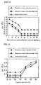
- FIG 9 shows the relation between the difference ⁇ T and each of contact area ratios (%) (5, 10, 20, 30, 40, 50 and 60) in case the plate 2 is supported on each pedestal 5 in contact with the end face, a portion inwardly away from the edge and the edge, respectively, thereof in the example 1.
- the contact area ratio is less than 30%
- the difference ⁇ T was almost constant and a homogeneous temperature distribution over the plate surface was maintained irrespectively of how the plate and pedestal were in contact with each other.
- the contact area ratio was over 30%
- the difference ⁇ T was suddenly larger and the homogeneity of plate-surface temperature distribution was low.
- FIG 10 shows the relation between the ratio between the pedestal height L and plate thickness and the difference ⁇ T in the example 1.
- the difference ⁇ T was smaller when the pedestal height was larger (when the plate was supported in air at a larger height).
- FIG 11 shows the relation between the contact area ratio and ⁇ T in the example 2.
- the example 2 showed almost the same tendency as that in FIG 9 for the example 1 although it used pedestals whose contact area ratio was within the range of 10 to 60 %.
- FIG 12 shows the relation between the ratio between the pedestal height L and plate thickness the difference ⁇ T in the example 2. As will be known from FIG 12, the relation is quite the same as in the example 1.
- FIG 13 shows the relation between the contact area ratio and ⁇ T in the example 3.
- the example 3 showed almost the same tendency as the examples 1 and 2 although it used a pedestal whose contact area ratio was within the range of 10 to 60 %.
- the difference ⁇ T was smaller when the pedestal 5 was in contact with the edge of the plate. Also, when the contact area ratio is over 30%, the difference ⁇ T is larger.
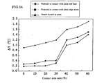
- FIG 14 shows the relation between the contact area ratio and ⁇ T in the example 4.
- the example 4 showed almost the same tendency as the examples 1 to 3 although it used a pedestal whose contact area ratio was within the range of 10 to 60 %.
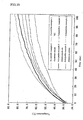
- the plate-surface temperature reached 65°C in 60 sec after start of the heating as will be known from FIG 15.
- the temperature rose at a higher rate as compared with those in the comparative examples 1 and 2. Therefore, the temperature rose appropriately.
- the test results show that the plate-surface temperature elevation in the acceptable example 4 in which the pedestals 5 were in contact with the four comers, respectively, of the plate 2 is best and both the highest temperature and temperature elevation rate are excellent. That is, it can be said that the supporting of the plate 2 on the pedestals 5 which are in contact with the four comers, respectively, is best.
- the plate-surface temperature has no yet reached 65 °C in 60 sec after the start of heating. Also, the plate-surface temperature rises slowly as compared with those in the acceptable examples 1 to 4. Namely, the heat is dissipated from the pedestal, which inhibits the plate-surface temperature from rising.
- Table 2 shows the relation between particle count and the ratio in area of contact between the pedestal and plate rear-side in the examples 1 to 4. As seen from Table 2, the particle count decreases considerably when the contact area ratio is less than 30%, especially under 25%.
- the temperature control element, and the temperature controller and waveguide type optical module, each using the temperature control element are superior in homogeneity of the plate-surface temperature distribution of the temperature control element, and in temperature elevation rate. Further, particles can be prevented from being separated in them. Therefore, the present invention can provide a waveguide type optical module having a superb optical waveguide characteristic supporting the multi-channeling, that is, having a stable wavelength demultiplexing characteristic.
Landscapes
- Physics & Mathematics (AREA)
- General Physics & Mathematics (AREA)
- Optics & Photonics (AREA)
- Engineering & Computer Science (AREA)
- Microelectronics & Electronic Packaging (AREA)
- Optical Integrated Circuits (AREA)
Abstract
A waveguide type optical module is provided which includes a temperature
control element supported on pedestals inside a casing, and an optical
waveguide provided on the temperature control element. The heating control
element includes a plate having a heater or heat absorber provided on a
non-heating side thereof or buried therein. The plate is supported on the
pedestals with less than 30% of the area thereof being in contact with the plate.
Because of such a structure, the waveguide type optical module has a good
wavelength demultiplexing characteristic, and the temperature controller and
control element for use in the optical module incur less occurrence of particle
separation and shows a high homogeneity of plate-surface temperature
distribution.
Description
The present invention relates to a waveguide type optical module, a
temperature controller and temperature control element for controlling the
temperature of an optical waveguide having a temperature-dependent
wavelength demultiplexing characteristic.
The conventional waveguide type optical module, especially, the
quartz-array waveguide type optical module with an optical wavelength
multi/demultiplexing function, uses a waveguide having a
temperature-dependent wavelength demultiplexing characteristic. The
waveguide type optical module of this type needs a temperature control of the
waveguide for maintaining a required wavelength demultiplexing characteristic.
Also an optical modulator or an optical switch, whose refractive index is
adjusted by changing the temperature for the optical deflection, should have the
temperature thereof adjusted for the refractive index not to vary. Both of these
requires a temperature controller for adjusting the temperature of the optical
waveguide.
Such a temperature controller is known from the disclosure in
JP-A-2001-116936. The disclosed temperature controller is used in a
quartz-array waveguide type optical module in which a heater is provided on a
plate, which appears as a ceramic substrate, whose thermal expansion coefficient
is 5 ppm/°C or less and thermal conductivity is 100 W/m·K or more, the plate is
held on a pedestal and an optical waveguide is formed on the plate.
The conventional waveguide type optical module is designed only for
providing a temperature controller made of a material having a small thermal
expansion coefficient and a good thermal conductivity. Therefore, the
temperature distribution is not homogeneous over the surface of the plate as the
temperature control element. Thus, the waveguide inevitably incurs a
distortion and has the wavelength demultiplexing characteristic thereof
degraded.
Also, with an increased number of waveguides, the waveguide fixed on the
plate has to be heated up to a predetermined temperature in a short time and held
at the temperature. However, since heat is not efficiently conducted from the
plate heated by a heater to the waveguide, so it is not possible to elevate the
temperature of the waveguide to higher than a certain point.
More specifically, heat generated by the heater is conducted partially to the
plate and also to the waveguide. The heat conducted to the plate will be
dissipated to the external space via the pedestal. Therefore, even if the heater
is designed to have an increased area and it is supplied with an increased amount
of electric power, the heat generated by the heater will not effectively be
conducted to the waveguide. So, the waveguide cannot be heated up to higher
than a certain point.
Thus, a wavelength which should be demultiplexed is not demultiplexed to
a core as a desired waveguide or causes optical signals to fail in functioning.
The present invention has a primary object to overcome the
above-mentioned drawbacks of the related art by providing a waveguide type
optical module suitable for a design having multiple optical waveguides and
excellent in wavelength demultiplexing characteristic.
The present invention has another object to provide a temperature
controller and temperature control element for use in the waveguide type optical
module, incurring less occurrence of a particle count and showing a highly
homogeneous distribution of temperature over the plate surface.
To overcome the drawbacks of the related art, the Inventors of the present
invention made many experiments and researches and found that when the area
of contact between the pedestal and plate was too large (32% or more), the
temperature distribution was not homogeneous over the plate of the temperature
control element and the temperature of the waveguide was not elevated to higher
than a certain point. Also, the Inventors found that by reducing the contact
area , the above drawbacks could be overcome and hence a waveguide type
optical module could be provided which is excellent in wavelength
demultiplexing characteristic.
The above object can be attained by providing a waveguide type optical
module including a temperature control element supported on pedestal inside a
casing, and an optical waveguide disposed in contact on the temperature control
element, wherein:
Also the above object can be attained by providing a temperature controller
for use in a waveguide type optical module, the temperature controller including
a temperature control element held inside a casing and which includes a plate
having a heater or heat absorber provided on a non-heating side thereof or
buried therein; and
there is installed to the plate a pedestal for supporting the plate thereon so that the area of contact with the pedestal and the non-heating side of the plate is less than 30% of the surface area of the plate.
there is installed to the plate a pedestal for supporting the plate thereon so that the area of contact with the pedestal and the non-heating side of the plate is less than 30% of the surface area of the plate.
Also the above object can be attained by providing a temperature control
element includes a plate having a heater or heat absorber provided on a
non-heating side thereof or buried therein, wherein the plate is shaped so that the
area of contact with a pedestal which support the plate thereon is less than 30%
of the surface area of the plate.
In each of the above products according to the present invention, each
pedestal should preferably be a one which is put into contact with the edge of
the plate to support the latter. Further, the pedestal should more preferably be a
one which is put into contact with the end face of the plate to support the latter.
Also, the plate should preferably be a ceramic-made one.
Also the above object can be attained by providing a waveguide type
optical module including a temperature control element supported on a pedestal
inside a casing, and an optical waveguide disposed in contact on the temperature
control element, wherein:
In the portion of each pedestal being in contact with the plate, when it is
assumed that one side of the plate is α1 while the length of the contacting
portion of the pedestal along the one side of the plate is α2, α2 should
preferably be 5 to 40 % of α1, the total area of the pedestal preferably be within
a range of 1 to 25 % of the surface area of the plate, and the area of each
pedestal preferably be within a range of 0.4 to 7 % of the surface area of the
plate.
According to the present invention, since the temperature control element
includes the plate having the heater or heat absorber on the non-heating side
thereof, or buried in, so the temperature of the plate can be increased and
decreased relatively uniformly over the plate surface. Especially in case the
heater or heat absorber is provided on the non-heating side (rear side) of the
plate, the heating can be made more homogeneously since heat will be
conducted while being dispersed over the plate surface when it is propagated to
a heating side of the plate. That is, since the plate functions to disperse the heat,
it is possible to prevent the heat from being distributed inhomogeneously due to
a wiring patter of the heater of heat absorber.
Note that since inside the casing, the plate is supported in air being isolated
by the pedestal from the bottom of the casing, so an air layer exists between the
plate itself and casing bottom, which provides an effect of heat insulation.
Thus, the plate is thermally insulated more effectively and homogeneous
temperature distribution on the heating side can be assured and temperature
elevation can be done at a higher rate.
According to the present invention, the area of contact between the pedestal
and rear side of the plate is less than about 30% of the rear surface area of the
plate, which is also intended for prevention of a cooling spot from being defined
on the plate. If the area of contact between the pedestal and plate rear side
exceeds 30% of the area surface area of the plate, the pedestal becomes a
conductor of heat to the casing and thus the heat is dissipated to outside from the
casing.
The area of contact between the pedestal and plate rear side should
preferably be 0.5 to 25 % of the rear surface area of the plate because the plate
made of ceramic, if applied, can incur less occurrence of a particle count as the
contact area is thus decreased. It should be noted that it is necessary to reduce
the particles adhering, if occur, to the end face of the waveguide and causing a
propagation loss.
Also, the plate should preferably be shaped to be generally rectangular and
be supported on the pedestal in contact with each outer comer thereof. In the
portion of the pedestal being in contact with the plate, when it is assumed that
one side of the plate has a length α1 while the contacting portion of each
pedestal along the one side of the plate has a length α2, α2 should preferably be
5 to 40 % of α1, the total area of the pedestal preferably be within a range of 1
to 25 % of the surface area of the plate, and the area of each pedestal preferably
be within a range of 0.4 to 6 % of the surface area of the plate.
With areas smaller than the above lower limits, the Inventors' reliability
tests proved that misalignment between the pedestal and plate caused
insufficient grounding and stability. On the other hand, with areas larger than
the above upper limits, the above reliability tests also proved that the
temperature of the plate could not be elevated slowly, not in a short time.
On this account, the pedestal is provided between the temperature control
element and casing to isolate the latter, and the area of contact between the
pedestal and plate is limited to as minimum as possible, thereby assuring a
homogeneous temperature distribution over the surface of the plate as a
temperature control element (heater plate) and a reduced time for heat elevation.
Note that the contact between the pedestal and plate may be an indirect
contact using an adhesive or the like alternatively of the aforementioned one.
In the waveguide type optical module-oriented temperature controller and
the waveguide type optical module itself according to the present invention, the
pedestal should preferably support the plate in contact with the edge (outer edge)
of the latter, and more preferably support the plate in contact with each outer
comer of the latter.
The reason for the above lies in the fact that with only the edge (outer edge)
of the plate (at the rear side) being in contact with the pedestal, heat dissipation
through the pedestal is smaller and it is possible to prevent inhomogeneous
temperature distribution over the plate. Further, with the plate being supported
on the pedestal in contact with each of four outer comers thereof, heat
dissipation through the pedestal is much smaller, so that heat conduction to the
optical waveguide can be more effective.
Also, when only the rear-side edge (outer edge) of the plate is put in
contact with the pedestal, a space is defined at the intermediate portion between
the pedestal and air can be caused to stay in this space for storage of heat. As
result, it is possible to effectively prevent inhomogeneous temperature
distribution over the surface of the plate.
Also, the plate may be supported on the pedestal with the end face thereof
placed on the pedestal. Generally, since the end face of the plate are exposed
to the fluidic atmosphere such as air, so heat is easily dissipated from there and
thus they will have the temperature thereof easily lowered. Thus, with the
plate being placed in contact at the end face thereof with on the pedestal, it is
possible to prevent the edge of the plate from being exposed to a highly fluidic
atmosphere and thus effectively prevent the temperature at the plate edge from
being lower.
These objects and other objects, features, and advantages of the present
invention will become more apparent from the following detailed description of
the preferred embodiments of the present invention when taken in conjunction
with the accompanying drawings. It should be noted that the present invention
is not limited to the embodiments but can freely be modified without departing
from the scope and spirit thereof defined in the claims given later.
The preferred embodiments of the present invention will be described
herebelow with reference to the accompanying drawings.
Referring now to FIG 1, there are illustrated in the form of a plan view the
temperature controller and temperature control element for use in the waveguide
type optical module according to the present invention. FIG. 2 is a sectional
view of the pedestal, FIGS. 3 and 4 are sectional side elevation and sectional
front view, respectively, of the temperature controller shown in FIG 1. As will
be seen from these drawings, the temperature control element for use in the
waveguide type optical module, generally indicated with a reference 1, typically
includes a plate 2 and a heater 3 disposed on a side (rear side) opposite to a
heating side of the plate 2 on which a waveguide is disposed. It should be
noted however that a Peltier element as a heat absorber may be provided in place
of the heater 3. Of course, the Peltier element has the functions of both the
heater and heat absorber.
On the area (inner) of the plate 2 where the heater 3 is formed, there are
provided pads 4 on which a thermistor chip and platinum resistance chip, used
for measurement of a temperature, are mounted, heater power lead wires 7 for
electrical connection with the pads 4, and thermistor lead wires 8. A thermistor
chip and platinum resistance chip are mounted on the pads 4 to measure a
temperature for the purpose of temperature control.
The plate 2 may be formed from a metal plate, ceramic plate, resin plate, or
the like. Examples of the metal plate include an aluminum plate, copper plate
and the like. Examples of the ceramic plate may include more than one
selected from among a nitride ceramics, carbide ceramics, oxide ceramics and
carbon. For example, since the nitride ceramics and carbide ceramics are
smaller in thermal expansion coefficient than the metal and considerably greater
in mechanical strength than the metal, a thin ceramic plate will not be warped or
distorted even when heated. Therefore, the plate 2 can be formed from a thin
and lightweight ceramic plate.
Further, such a ceramic plate is characterized in that the surface
temperature thereof will quickly respond to a change in temperature of a
resistance heater because of the high heat conductivity and small thickness of
the ceramic plate.
Therefore, the ceramic plate can advantageously have the surface
temperature thereof controlled when changing the temperature of the resistance
heater by changing the voltage or current supplied to the heater.
Note that the nitride ceramics may be aluminum nitride, silicon nitride,
boron nitride, titanium nitride or the like, for example, and they may be used
singly or more than two of them be used in combination. Also, it should be
noted that the carbide ceramics may be silicon carbide, boron carbide, titanium
carbide, tantalum carbide, tungsten carbide or the like, for example and they
may be used singly or more than two of them be used in combination.
Among the above materials, the aluminum nitride is most preferable for
forming the plate 2 because it has a highest heat conductivity as 180 W/m.K and
it is outstanding in temperature response.
Also, since the ceramic used as a material for the plate 2 shows a small
thermal expansion coefficient and has only a small difference in thermal
expansion from a waveguide 12 even when the temperature becomes high, the
waveguide 12 will not be broken and separated from the temperature control
element (plate) 1.
At the center inside a casing 9, the plate 2 is supported in air on a pedestal
5 shaped like a square frame (square column) in contact with the rear-side edge
(outer edge) thereof. As shown in FIGS. 2 to 4, the pedestal 5 is cut out except
for the edge thereof to form a step 5a (on which the edge of the plate 2 is placed).
Namely, the pedestal 5 is countersunk at the upper side thereof except for the
edge thereof. The plate 2 is fixed by fitting along the edge thereof to the step
5a and remaining top end of the pedestal 5 so that the upper surface of the plate
2 will be flush with the upper surface of the pedestal 5. Therefore, the stepped
portion (5a) of the pedestal 5 will be in contact with both the rear-side edge
(outer edge) and end face of the plate 2.
On the pedestal 5, there should preferably be formed a lead-in port for
leading out the lead wires 7 for supplying power to the heater 3 or heat absorber
and the lead wires 8 for supplying power to the thermistor chip. That is to say,
all the rear-side edge (outer edge) of the plate 2 may not be in contact with the
pedestal 5. It should be noted that the plate 2 should preferably be fixed with
fixtures 6 to the pedestal 5.
FIGS. 3 and 4 are axial sectional views of the temperature controller whose
temperature control element 1 is fixed to the pedestal 5. As shown, the
temperature controller according to the present invention has the plate 2 wholly
fixed by fitting to the step 5a in the pedestal 5. The temperature controller of
the aforementioned structure is fixed in air on the pedestal 5 inside the casing 9.
The pedestal 5 may be located inside a heater wiring area and at the rear
side of the plate 2 as shown in FIG 5, or outside the heater wiring area and at the
rear-side edge (outer edge) of the plate 2 as shown in FIG. 6. However, the
plate 2 should more preferably be supported in air on the pedestal 5 in contact
with the edge (outer edge) of the plate 2 than in contact with the rear side of the
plate 2 inside the heater wiring area because the temperature is distributed more
homogeneously over the surface of the plate 2.
In case the plate 2 is put in contact at the rear-side edge thereof (outer edge)
with the pedestal 5 outside the heater wiring area, the distance from the heater 3
to the pedestal 5 over which the heat is conducted is so longer that the heat will
be dispersed more and the amount of heat per unit area will be smaller. As the
result, even if the plate is in contact at the same ratio of area with the pedestal 5,
the amount of heat conducted to the pedestal 5 will also be smaller.
Also, since the plate 2 is fixed by fitting at the edge thereof to the step 5a
formed in the upper portion of the frame-shaped pedestal 5, the edge of the plate
2 is not exposed to any fluidic atmosphere like air and the heat is stored with an
improved efficiency, so that the heat will be distributed more homogeneously
over the surface of the plate 2.
The pedestal 5 should advantageously be structured to have four square
columns which are in contact with four rear-side comers, respectively, of the
plate 2 as shown in FIG 7. The sum S0 (= S1 + S2 + S3 + S4) of sectional
areas of the square columns, which are in contact with the plate 2, should
desirably be less than 30% of the rear side area S of the plate 2, more desirably
be within a range of 0.5 to 30 % of S, and most desirably be within a range of 4
to 25 % of S.
The reason for the above lies in the fact that when the sum of sectional
areas exceeds 30%, heat is propagated to the casing and dissipated, which will
influence the temperature elevation.
The columns are not limited in shape to the square but they may be formed
as a circular or elliptical cylinder which can support the plate 2 in contact with
the rear side of the latter.
The shape of the pedestal is not limited in shape to the above square
column, but it may be circular cylinder, elliptic cylinder or the like. The
pedestal shape may be a one which assures the sum S0 of sectional areas of the
pedestal which are in contact with the rear side of the plate 2 to be within the
above-mentioned range.
Also, the sectional areas (S1, S2, S3 and S4) of the four square columns,
which are to be in contact with the plate, should desirably be within a range of
0.4 to 7 % of the rear side area S of the plate for the reason that when the contact
sectional area is below 0.4%, the pedestals cannot support the plate stably while
a contact sectional area of above 7% will influence the temperature elevation.
Also, in case the plate 2 has a square section (one side has a length α1) and
each of the square columns has a square section (one side has a length α2), it is
desirable that 0.05 ≤ α2/α1 ≤ 0.4 because the α2/α1 ratio of less than 0.05 (5%)
will not assure any stable support of the plate while the ratio of more than 0.4
(40%) will influence the temperature elevation.
The plate 2 should desirably have a thickness of 0.1 to 10 mm. This is
because if the plate thickness is over 10 mm, the plate 2 will have a larger heat
capacity so that the temperature distribution over the plate surface will not be
homogeneous while a plate thickness of less than 0.1 mm will cause a
homogeneous temperature distribution approximate to those on the heater or
heat absorber, also leading to an inhomogeneous temperature distribution.
The thickness 1 of the plate 2 and height L of the pedestal 5 should
desirably be in a relation of approximately L ≥ 2.5 × 1. If the relation is L < 2.5
× 1, the heat insulation or heat storage by the air layer will be insufficient.
According to the present invention, it is desirable that 1 = 0.635 mm and L = 3.2
mm.
The pedestal 5 may be formed from ceramic, metal or resin or the like but
the heat conductivity of such a material should desirably be less than 50 W/m·K
which will not lead to any heat conduction-caused occurrence of a homogeneous
temperature distribution on the plate. The ceramics may be an alumina, quartz,
cordierite or the like. Also, even when a silicon carbide (SiC) or aluminum
nitride (AlN), having a high heat conductivity, is used to form the pedestal 5, the
heat conductivity can be lowered by processing this material into a porous one.
The metal may be a one whose heat conductivity is low, such as a nickel (Ni)
alloy. Further, the resin may be glass epoxy or glass polyimide. In this case,
the pedestal 5 is formed by punching and countersinking the resin substrate.
According to the present invention, the heater 3 may be formed on the
non-heating side (rear side) of the plate 2 or buried in the plate 2. In case the
heater 3 is formed buried in the plate 2, it should desirably be formed at a depth
of less than 60% of the plate thickness from the side of the plate opposite to the
heating side (far from the heating side). If it is buried at a depth of more than
60%, namely, if it is positioned too near to the heating side, the heat in the plate
2 will not sufficiently be dissipated, causing an inhomogeneous temperature
distribution on the heating side.
In case the heater 3 is formed buried in the plate 2 as above, a plurality of
heater layers may be provided. In this case, the pattern of each layer should
desirably be such that a resistance heater is formed in any of the layers and each
layer appears to include one resistance heater when viewed from the heating side
of the plate 2. Such a pattern may be a zigzag layout, for example.
Note that the heater 3 may be buried in the plate 2 and partially exposed to
outside the plate 2.
Note that in case the heater 3 is formed on the surface of the plate 2, it is
preferable that a conductive paste containing metal particles should be applied to
the surface of the plate 2 to form a conductive paste layer having a
predetermined pattern, and then the conductive paste pattern be baked to sinter
the metal particles on the plate surface. It should be noted that the metal
sintering may be such that the metal particles, and the metal particles and
ceramics, are welded to each other.
In case the heater 3 is buried in the plate 2, its thickness should preferably
be within a range of 1 to 50 µm. When the heater 3 is to be formed on the
surface of the plate 2, its thickness should preferably be within a range of 1 to 30
µm, and more preferably within a range of 1 to 10 µm.
In case the heater 3 is formed buried in the plate 2, its width should
preferably be within a range of 5 to 20 µm. On the other hand, in case the
heater 3 is formed on the surface of the plate 2, its width should preferably be
within a range of 1 to 20 mm, and more preferably within a range of 0.1 to 5
mm.
The heater 3 can be varied in resistance by changing its width and thickness.
However, the aforementioned thickness and width are most practical ones. The
smaller the thickness and width, the higher the resistance becomes. In this
respect, when it is formed buried in the plate, the heater can be thicker and wider
but the surface temperature distribution will be correspondingly inhomogeneous.
In this case, it is necessary to design the heater which has an increased width.
Also, since the heater is buried in the plate, no consideration has to be paid to
the adherence to the nitride ceramics or the like, the heater 3 may be formed
from a high melting-point metal such as tungsten, molybdenum or the like or a
carbide such as a carbide of tungsten, molybdenum or the like, and thus the
resistance of the heater 3 can be increased. Therefore, the heater 3 may be
formed thick against breakage. Accordingly, the heater 3 should desirably be
formed to have the aforementioned thickness and width.
With the heater being positioned as above, as the heat generated by the
heater is propagated, it will be dispersed to the entire plate and the temperature
will be distributed homogeneously over the side thereof heating the waveguide.
The heater may have a sectional form, either rectangular or elliptic but the
section should desirably be flat since this form contributes to an easier heat
dissipation toward the heating side of the plate and a homogeneous temperature
distribution on the heating side. Also, the material of the resistance heater is
not limited to the conductive paste but it should preferably contain resin, solvent,
thickener, etc. in addition to metal particles or conductive ceramics which add to
an electro-conductivity of the heater.
The metal particles as a material of the heater 3 should desirably be a noble
metal (such as gold, silver, platinum or palladium), lead, tungsten, molybdenum,
nickel or the like. Among others, the material should more preferably be one
of the noble metals (gold, silver, platinum and palladium). These metals may
be used singly or in combination, but more than two of them should desirably be
used in combination since they are not easily oxidizable and has a sufficient
resistance for heat generation. The above-mentioned conductive ceramics
include carbides of tungsten and molybdenum. These ceramics may be used
singly or more than two of them be used in combination.
Also, the size of the metal or ceramic particles should preferably be within
a range of 0.1 to 100 µm. If the size is less than 0.1 µm, the particles are easily
oxidizable. On the other hand, the particles of more than 100 µm in size are
not easy to sinter and have a higher resistance.
The metal particles may be either globular or squamate, or may include
globular and squamate ones. The squamate or globular/squamate metal
particles can hold metal oxide between them, and contribute to a positive
adherence between the resistance heater and nitride ceramics or the like as well
as to an increase resistance of the heater.
The resins usable to make the conductive paste includes epoxy resin,
phenol resin, etc., for example. Also, the solvent may be isopropyl alcohol or
the like, for example. The thickener may be cellulose or the like. The
conductive paste should desirably be formed by adding a metal oxide to metal
particles and sintering the metal particles and metal oxide. By sintering the
metal oxide along with the metal particles, the metal particles can be made to
adhere to the nitride ceramics (ceramic substrate) or carbide ceramics. By
mixing the metal oxide in the conductive paste in this way, the adherence of the
paste to the nitride ceramics or carbide ceramics can be improved although the
reason is not known exactly. Presumably, the surface of each metal particle
and nitride or carbide ceramics is slightly oxidized to form an oxide film and
thus the oxide films are integrated with each other via the metal oxide when the
materials are sintered, so that the metal particles and nitride or carbide ceramics
will adhere to each other.
The metal oxide should preferably be at least one selected from a group of
lead oxide, zinc oxide, silica, boron oxide (B2O3), alumina, yttria and titania, for
example. These oxides permits to improve the adherence between the metal
particles and nitride or carbide ceramics without increasing the resistance of the
resistance heater. When the total amount of the metal oxide is taken as 100%
by weight, the amounts of the above-mentioned metal oxides, namely, lead
oxide, zinc oxide, silica, boron oxide (B2O3), alumina, yttria and titania should
desirably be adjusted to 1 to 10 % by weight, 20 to 70 % by weight, 1 to 30 %
by weight, 5 to 50 % by weight, 1 to 10 % by weight, 1 to 50 % by weight and 1
to 50 % by weight, respectively, with the sum thereof being not over 100% by
weight. By adjusting the amounts of these oxides within the above ranges,
respectively, it is possible to improve the adherence of the metal particles,
especially with the nitride ceramics.
The addition of the metal oxide to the metal particles should preferably be
within a range over 0.1% by weight and under 10% by weight. Also, the heater
may be formed from a metal foil or wire. The metal foil may be a nickel foil or
stainless steel foil. It should desirably be etched to form a pattern of the
resistance heater. The metal foils thus patterned may be attached to each other
to form the resistance heater. The metal wire may be a tungsten or
molybdenum wire, for example.
In case the heater is formed on the surface of the plate 2, a metal coating
layer should desirably be formed on the surface of the heater in order to prevent
the internal sintered metal from being oxidized and having the resistance thereof
changed. The metal coating layer should preferably be 0.1 to 10 µm thick.
The metal used to for the metal coating layer is not limited to any special one
but it may be any metal which is non-oxidizable. More specifically, the metal
may be gold, silver, palladium, platinum, nickel or the like, for example. These
metals may be used singly or two or more of them be used in combination.
Among others, nickel should preferably be used to form the metal coating layer.
The heater has to be connected to the lead wires 7 for connection to the
power source. The connection is made by soldering or brazing. A heat
absorber may be used instead of the heater having previously been described.
In this case, the heat absorber may be a Peltier element. The Peltier element
may be connected to the lead wires 7 with an adhesive or any physical means
such as screw or spring.
Referring now to FIG 8, there is illustrated in the form of a sectional view
a typical embodiment of the waveguide type optical module according to the
present invention. As shown, the waveguide type optical module generally
indicated with a reference 100 includes primarily the aforementioned
temperature controller composed of the temperature control element 1 and
pedestal 5, Y-branched waveguide 12 and casing 11. The waveguide 12 is
connected to an input optical fiber 9 and output optical fiber 9', for example, to
multiplex and demultiplex the light. The waveguide 12 should advantageously
be a quartz-array waveguide of which the wavelength demultiplexing
characteristic varies depending upon the temperature. It should be noted that in
FIG 8, references 10 and 10' indicate fiber fixtures.
The casing 11 is of a box-shaped structure having a lead-out port through
which the input and output optical fibers 9 and 9' and lead wires 7 and 8 are led
out. Inside the casing 11, the temperature control element 1 is supported in air
on the pedestal 5 and the waveguide 12 is fixed in contact on the heating side
surface of the temperature control element 1.
Because of such a structure of the waveguide type optical module 100, the
heat homogeneously distributed over the plate surface of the temperature control
element 1 can homogeneously be conducted to the waveguide 12 in a short time,
whereby the heat dissipation and power consumption can considerably be
reduced. Thus, the wavelength variation in the wavelength demultiplexing
characteristic of the waveguide 12 can be limited to positively stabilize the
wavelength demultiplexing characteristic.
In the foregoing, some embodiments of the present invention have been
described. However, the present invention is not limited to such embodiments
but can be modified or altered in various forms. For example, the optical
waveguide 12 may be formed from polyimide fluoride or the like in addition to
the aforementioned quartz, and the light may be a semiconductor laser light.
Also, the optical waveguide 12 and temperature control element 1 may be
joined to each other with a mechanical fixture such as screw or spring in
addition to the adhesive.
The present invention will be described in further detail concerning
examples of the waveguide type optical module.
(1) There was prepared a paste formed from a mixture of aluminum
nitride powder (by Tokuyama, 1.1 µm in mean particle size) in 100% by weight,
yttrium oxide (Y2O3): yttria, 0.4 µm in mean particle size) in 4% by weight,
acrylic resin binder in 11.5% by weight, dispersant in 0.5% by weight and
alcohol of 1-butanol and ethanol in 53% by weight. It was dry-sprayed.
Granules thus produced were filled in a mold to form a raw molding of 1.5 mm
in thickness. The raw molding was sintered in a nitrogen atmosphere at a
temperature of 1890°C for 3 hours under a pressure of 200 kg/m2. Thereafter,
the sintered product was cut into a square ceramic plate 2 (for a substrate of the
temperature control element) of 0.64 mm in thickness and 50.3 mm in side
length.
(2) On the non-heating side (rear side) of the ceramic plate 2 prepared as
above, there was formed a conductive paste layer for the heater 3 by screen
printing. The heating pattern by the printed conductive paste was as shown in
FIG. 1. The conductive paste used was a composition of Ag in 48% by weight,
Pt in 21% by eight, SiO2 in 1.0% by weight, B2O3 in 1.2% by weight, ZnO in
4.1 % by weight, PbO in 3.4 % by weight, ethyl acetate in 3.4% by weight and
butyl carbinol in 17.9% by weight. The conductive paste is an Ag-Pt paste in
which silver particles were 4.5 µm in mean particle size and squamate and Pt
particles were 0.5 µm in mean particle size.
(3) After a pattern of the heater was formed from the conductive paste,
the ceramic plate 2 was heated and calcinated at 780°C to sinter Ag and Pt in the
conductive paste while baking the paste to the surface of the ceramic plate 2, to
thereby form a so-called resistance heater 3 and thermistor circuit. The
resistance heater 3 has a thickness of 5 µm and width of 2.4 mm and a sheet
resistivity of 7.7 mΩ/□.
(4) The ceramic plate 2 prepared in above step (3) was immersed in an
electroless nickel-plating bath filled with an aqueous solution containing 80 g/l
of nickel sulfate, 24 g/l of sodium hypophosphite, 12 g/l of sodium acetate, 8 g/l
of boric acid and 6 g/l of ammonium chloride to deposit a metal coating layer
(nickel layer) of 1 µm in thickness on the surfaces of the silver resistance heater
3, thermistor circuit and thermistor pad.
(5) A solder paste was printed on the thermistor pad, and a thermistor was
placed on the solder paste over the thermistor pad. The thermistor and
thermistor pad were heated to 200°C to mount the thermistor on the thermistor
pad. Further, the lead wires 7 and 8 were connected by brazing to the
thermistor circuit and heater circuit to form the temperature control element 1
(ceramic heater).
(6) Next, a glass epoxy substrate (by Matsushita Electric Works, FR-4)
was cut into a square piece. The epoxy substrate piece was punched at the
center thereof to form a square frame, and the square frame was countersunk
except for the edge thereof to a depth of about 0.64 mm at the upper side along
the edge thereof using a drill to form a pedestal 5 with a step 5a.
The pedestal 5 with the step 5a was used to support the temperature control
element 1 prepared in above step (5). The ceramic plate 2 was fixed by fitting
at the edge thereof to the step 5a.
Note that a lead-out port for leading out the lead wires 7 and 8 was formed
at the same time by countersinking.
(7) The temperature control element 1 (ceramic heater) fixed by fitting to
the step 5a of the pedestal 5 was fixed at the diagonal comers thereof with a
glass epoxy fixture (retainer 6) to form a temperature controller.
(8) Further, the temperature controller (pedestal 5) was fixed by bonding
with an adhesive in the box-shaped stainless steel casing 11, and a Y-branched
quartz-array optical waveguide 12 was put over the temperature control element
1 and fixed with a silicon resin adhesive to the latter. Thus, a waveguide type
optical module was formed.
(a) To test the example 1 for the homogeneity of plate-surface
temperature distribution, the glass epoxy substrate was punched in the center
thereof to form an opening there. By punching the glass epoxy substrate to
form an opening of another diameter, and repeating such punching, to change
the opening area, the area of contact between the pedestal 5 and ceramic plate 2
was changed from 5 to 60 % of the rear-surface area of the ceramic plate 2.
More specifically, several types of the pedestal 5 were prepared in which
the ratios in area of contact between the pedestal 5 and ceramic plate 2 with the
rear-surface area of the ceramic plate 2 (will be referred to simply as "contact
area ratio" hereunder) were within a range of 5 to 60 %. The homogeneity of
plate-surface temperature distribution was measured with the ceramic plate 2
supported on each of the pedestals 5 different in contact area ratio from each
other.
In the example 1, the pedestal 5 was in contact with the ceramic plate 2 at
the edge and end face of the latter (will be referred to as "end face" hereunder).
In addition to the pedestals which were in contact with the ceramic plate as
above, there were prepared a pedestal which was in contact with the plate 2 at an
inner portion of the latter (nearer to the center) (as shown in FIG 5) and a
pedestal which was in contact with the plate 2 at the edge of the latter (as shown
in FIG. 6). Several types of such pedestals 5 each having contact area ratios of
5 to 60 % were prepared. The homogeneity of plate-surface temperature
distribution was measured with the ceramic plate 2 supported on each of such
additional pedestals 5.
Note that the pedestals each having a contact area ratio of less than 30%
were taken as acceptable ones while the pedestals each having a contact area
ratio of more than 30% were taken as comparative ones.
(b) Also, with the height of the plate 2 supported on the pedestal 5
inside the casing 11 being adjusted, the plate-surface temperature distribution
was measured using a thermo-viewer set to 80°C and a difference ΔT was
calculated between highest and lowest temperatures over the plate surface.
Note that in case no pedestal 5 was used, namely, in case the plate 2 was
placed in direct contact with the casing 11, the temperature difference ΔT was
3°C.
(c) Further, the number of particles appearing separated from the
ceramic adhering to the waveguide 12 was counted. For this measurement, ten
freely-selected places on the surface of the waveguide 12 were photographed by
an electron microscope, and the particles in each place were counted. The
numbers of particles counted in the ten places were averaged as a particle count.
The example 2 was tested under basically same conditions as in the testing
on the example 1 except that a Peltier element was used instead of the heater 3.
The Peltier element was fixed with an epoxy resin adhesive to the plate. Also,
since cooling, not heating, was made in this example 2, the homogeneity of
plate-surface temperature distribution was measured by calculating the
difference ΔT between highest and lowest temperatures with the thermo-viewer
set to 5°C.
The example 3 was tested under basically same conditions as in the testing
on the example 1 except that the plate was formed from silicone carbide, not
from the aluminum nitride.
A paste was prepared from a mixture of silicon carbide (by Yakushima
Electric, 1.1 µm in mean particle size) in 100% by weight, B4C (1 µm in mean
particle size) in 4% by weight, acrylic resin binder in 11.5% by weight,
dispersant in 0.5% by weight and alcohol containing 1-buthanol and ethanol in
53% by weight. It was molded by the doctor blade method to form a plurality
of raw moldings of 0.47 mm in thickness.
Next, the raw moldings were dried at 80°C for 5 hours, and were punched
to form a portion which would be a lead-out port through which connection is to
be made external terminals.
Then, a conductive paste formed from a mixture of tungsten carbide
particles of 1.1 µm in mean particle size in 100% by weight, acrylic resin binder
in 3.0% by weight, α-terpineol solvent in 3.5% by weight and dispersant in
0.3% by weight was filled in the punched portion for the lead-out port in the raw
moldings to form a conductive paste layer for a wiring pattern and a pad on
which a heater 3 and thermistor were to be mounted.
Next, the raw moldings were stacked one on another. The stack was
sintered by heating in a nitrogen atmosphere at 1980°C under a pressure of 200
kg/cm2 to form a ceramic plate 2. Then the ceramic plate 2 was cut for the
mounting pad to be exposed to outside, and a thermistor was mounted on the
pad to form a temperature control element 1 of 1.5 mm in thickness.
The example 4 was tested under basically same conditions as in the testing
on the example 1 except that the pedestal 5 was designed to support the ceramic
plate 2 at four outer comers of the latter.
Namely, a glass epoxy substrate (by Matsushita Electric Works, FR-4) of
3.3 mm in thickness was cut into a square piece of 20 mm by 20 mm in
dimensions. The epoxy substrate piece was punched at the center thereof to
form a square frame, and the square frame was countersunk except for the edge
thereof to a depth of about 0.64 mm at the upper side along the edge thereof
using a drill to form four pedestals 5 each with a step 5a, identical in shape to
each other and having dimensions of 10 mm by 10 mm. The pedestals 5 were
fixed by bonding to an epoxy substrate somewhat larger than the ceramic plate 2
in a geometry in which they correspond to the four comers, respectively, of the
ceramic plate 2.
After fixing, by fitting, the ceramic plate 2 at the four corners thereof to the
steps 5a, respectively, of the pedestals 5, the comers were fixed each with an
epoxy resin fixture (retainer 6) to form a temperature controller.
Further, the temperature controller (pedestal 5) was fixed by bonding with
an epoxy resin adhesive in the box-shaped stainless steel casing 11, and a
Y-branched quartz-array optical waveguide 12 was put over the temperature
control element 1 and fixed with a silicon resin adhesive to the latter. Thus, a
waveguide type optical module was formed.
In the testing on the aforementioned examples 1 to 4, the highest and
lowest plate-surface temperatures were measured and a difference ΔT between
the temperature was calculated. The results are shown in FIGS. 9 to 14.
FIG 9 shows the relation between the difference ΔT and each of contact
area ratios (%) (5, 10, 20, 30, 40, 50 and 60) in case the plate 2 is supported on
each pedestal 5 in contact with the end face, a portion inwardly away from the
edge and the edge, respectively, thereof in the example 1.
In the acceptable examples in which the contact area ratio is less than 30%,
the difference ΔT was almost constant and a homogeneous temperature
distribution over the plate surface was maintained irrespectively of how the plate
and pedestal were in contact with each other. However, in comparative
examples in which the contact area ratio was over 30%, the difference ΔT was
suddenly larger and the homogeneity of plate-surface temperature distribution
was low.
FIG 10 shows the relation between the ratio between the pedestal height L
and plate thickness and the difference ΔT in the example 1. As will be known
from the graphically illustrated relation, the difference ΔT was smaller when the
pedestal height was larger (when the plate was supported in air at a larger
height).
FIG 11 shows the relation between the contact area ratio and ΔT in the
example 2. The example 2 showed almost the same tendency as that in FIG 9
for the example 1 although it used pedestals whose contact area ratio was within
the range of 10 to 60 %.
FIG 12 shows the relation between the ratio between the pedestal height L
and plate thickness the difference ΔT in the example 2. As will be known from
FIG 12, the relation is quite the same as in the example 1.
FIG 13 shows the relation between the contact area ratio and ΔT in the
example 3. The example 3 showed almost the same tendency as the examples
1 and 2 although it used a pedestal whose contact area ratio was within the range
of 10 to 60 %.
Note that as seen from FIGS. 9, 11 and 13, the difference ΔT was smaller
when the pedestal 5 was in contact with the edge of the plate. Also, when the
contact area ratio is over 30%, the difference ΔT is larger.
FIG 14 shows the relation between the contact area ratio and ΔT in the
example 4. As seen, the example 4 showed almost the same tendency as the
examples 1 to 3 although it used a pedestal whose contact area ratio was within
the range of 10 to 60 %.
Further, an example in which the contact area ratio was under 30% was
selected from of each of the above four examples 1 to 4 (these selected examples
will be referred to as "acceptable examples 1 to 4" hereunder), and also an
example in which the contact area ratio was over 30% was selected from each of
the examples 1 and 2 (these selected examples will be referred to as
"comparative examples 1 and 2" hereunder). These selected acceptable and
comparative examples were tested for the plate-surface temperature elevation
rate. The test results are shown in Table 1 and FIG 15.
- Acceptable example 1:
- 635.04 mm2 in contact area, and 25.1 % in contact area ratio
- Acceptable example 2:
- 750 mm2 in contact area, and 29.6% in contact area ratio
- Acceptable example 3:
- 533.6 mm2 in contact area, and 21.1% in contact area ratio
- Acceptable example 4:
- 256 mm2 in contact area (64 mm2 × 4), and 10.1 % in contact area ratio
- Comparative example 1:
- 2052 mm2 in contact area, and 81.1% in contact area ratio
- Comparative example 2:
- 811 mm2 in contact area, and 32.1% in contact area ratio
The above temperature elevation test was done at the normal temperature
(about 25°C). The prepared module was placed on a heat-resistant resin plate
(phenyl Bakelite), a thermo-sensor was installed to the module surface, and the
temperature (°C) was measured for an energization time length (sec) after a
power of 8 W was supplied to the ceramic heater.
| Material | Contact area ratio (%) | Plate-surface temperature in 60 sec (°C) | |
| Acceptable example 1 | Aluminum nitride | 25.1 | 76.2 |
| Acceptable example 2 | Aluminum nitride | 29.6 | 71.2 |
| Acceptable example 3 | Silicon carbide | 21.1 | 66.2 |
| Acceptable example 4 | Aluminum nitride | 10.1 | 68.9 |
| Comparative example 1 | Aluminum nitride | 80.1 | 56.1 |
| Comparative example 2 | Aluminum nitride | 32.1 | 64.1 |
In the acceptable examples 1 to 4 according to the present invention, the
plate-surface temperature reached 65°C in 60 sec after start of the heating as will
be known from FIG 15. As will also be seen, after having reached 60°C, the
temperature rose at a higher rate as compared with those in the comparative
examples 1 and 2. Therefore, the temperature rose appropriately. Further, the
test results show that the plate-surface temperature elevation in the acceptable
example 4 in which the pedestals 5 were in contact with the four comers,
respectively, of the plate 2 is best and both the highest temperature and
temperature elevation rate are excellent. That is, it can be said that the
supporting of the plate 2 on the pedestals 5 which are in contact with the four
comers, respectively, is best.
In the comparative examples 1 and 2, however, the plate-surface
temperature has no yet reached 65 °C in 60 sec after the start of heating. Also,
the plate-surface temperature rises slowly as compared with those in the
acceptable examples 1 to 4. Namely, the heat is dissipated from the pedestal,
which inhibits the plate-surface temperature from rising.
Table 2 shows the relation between particle count and the ratio in area of
contact between the pedestal and plate rear-side in the examples 1 to 4. As
seen from Table 2, the particle count decreases considerably when the contact
area ratio is less than 30%, especially under 25%.
| Contact area ratio (%) | Particle count (particles/cm2) |
| 0.5 | 100 |
| 5 | 110 |
| 10 | 120 |
| 15 | 123 |
| 20 | 125 |
| 25 | 123 |
| 30 | 829 |
| 40 | 1320 |
| 50 | 1303 |
| 60 | 2031 |
As having been described in the foregoing, the temperature control element,
and the temperature controller and waveguide type optical module, each using
the temperature control element, are superior in homogeneity of the
plate-surface temperature distribution of the temperature control element, and in
temperature elevation rate. Further, particles can be prevented from being
separated in them. Therefore, the present invention can provide a waveguide
type optical module having a superb optical waveguide characteristic supporting
the multi-channeling, that is, having a stable wavelength demultiplexing
characteristic.
Claims (18)
- A waveguide type optical module comprising a temperature control element supported on a pedestal inside a casing, and an optical waveguide disposed in contact on the temperature control element, wherein:the temperature control element includes a plate having a heater or heat absorber provided on a non-heating side thereof or buried therein; andthe plate is supported inside the casing so that the area of contact with the pedestal is less than 30% of the surface area of the plate.
- The optical module according to claim 1, wherein the pedestal is put into contact with the edge of the plate to support the latter.
- The optical module according to claim 1 or 2, wherein the pedestal supports the plate in contact with the end face of the latter.
- The optical module according to any of claims 1 to 3, wherein the plate is made of ceramics.
- A temperature controller for use in a waveguide type optical module, the temperature controller comprising a temperature control element held inside a casing and which includes a plate having a heater or heat absorber provided on a non-heating side thereof or buried therein; and
there is installed to the plate a pedestal for supporting the plate thereon so that the area of contact with the pedestal and the non-heating side of the plate is less than 30% of the surface area of the plate. - The temperature controller for use in a waveguide type optical module according to claim 5, wherein the pedestal is put into contact with the edge of the plate to support the latter.
- The temperature controller for use in a waveguide type optical module according to claim 5 or 6, wherein the pedestal supports the plate in contact with the end face of the latter.
- The temperature controller for use in a waveguide type optical module according to any of claims 5 to 7, wherein the plate is made of ceramics.
- A waveguide type optical module comprising a temperature control element supported on a pedestal inside a casing, and an optical waveguide disposed in contact on the temperature control element, wherein:the temperature control element includes a generally rectangular plate having a heater or heat absorber provided on a non-heating side thereof or buried therein; andthe pedestal supports the plate thereon in contact with each outer comer of the latter and so that the area of contact between the pedestal and plate is less than 30% of the surface area of the plate.
- The optical module according to claim 9, wherein in the portion of each pedestal being in contact with the plate, when it is assumed that one side of the plate is α1 while the length of the contacting portion of the pedestal along the one side of the plate is α2, α2 should preferably be 5 to 40 % of α1.
- The optical module according to claim 9, wherein the total area of the pedestal preferably be within a range of 1 to 25 % of the surface area of the plate.
- The optical module according to claim 9, wherein the area of each pedestal preferably be within a range of 0.4 to 7 % of the surface area of the plate.
- The optical module according to claim 9, wherein the pedestal supports the plate in contact with the end face of the latter.
- The optical module according to claim 9, wherein the plate is made of ceramics.
- A temperature control element including a plate having a heater or heat absorber provided on a non-heating side thereof or buried therein, wherein the plate is shaped so that the area of contact with a pedestal which support the plate thereon is less than 30% of the surface area of the plate.
- The temperature control element according to claim 15, wherein the pedestal is put into contact with the edge of the plate to support the latter.
- The temperature control element according to claim 15 or 16, wherein the pedestal supports the plate in contact with the end face of the latter.
- The temperature control element according to any of claims 15 to 17, wherein the plate is made of ceramics.
Applications Claiming Priority (5)
| Application Number | Priority Date | Filing Date | Title |
|---|---|---|---|
| JP2002015929 | 2002-01-24 | ||
| JP2002015929 | 2002-01-24 | ||
| JP2002367051 | 2002-12-18 | ||
| JP2002367051A JP2003287631A (en) | 2002-01-24 | 2002-12-18 | Waveguide type optical module, and temperature control component and temperature control element thereof |
| PCT/JP2003/000300 WO2003062877A1 (en) | 2002-01-24 | 2003-01-16 | Waveguide type optical module, and temperature control component, and temperature control element thereof |
Publications (2)
| Publication Number | Publication Date |
|---|---|
| EP1475651A1 true EP1475651A1 (en) | 2004-11-10 |
| EP1475651A4 EP1475651A4 (en) | 2006-08-09 |
Family
ID=27615694
Family Applications (1)
| Application Number | Title | Priority Date | Filing Date |
|---|---|---|---|
| EP03701735A Withdrawn EP1475651A4 (en) | 2002-01-24 | 2003-01-16 | Waveguide type optical module, and temperature control component, and temperature control element thereof |
Country Status (5)
| Country | Link |
|---|---|
| US (1) | US20050078919A1 (en) |
| EP (1) | EP1475651A4 (en) |
| JP (1) | JP2003287631A (en) |
| TW (1) | TW200302364A (en) |
| WO (1) | WO2003062877A1 (en) |
Families Citing this family (3)
| Publication number | Priority date | Publication date | Assignee | Title |
|---|---|---|---|---|
| JP4467280B2 (en) * | 2003-10-22 | 2010-05-26 | 富士通株式会社 | Optical device module |
| US9645333B2 (en) * | 2014-10-17 | 2017-05-09 | Lumentum Operations Llc | Optomechanical assembly |
| CN205287021U (en) * | 2015-11-18 | 2016-06-08 | 马笑远 | Fragrance stove |
Family Cites Families (5)
| Publication number | Priority date | Publication date | Assignee | Title |
|---|---|---|---|---|
| JPH09101430A (en) * | 1995-10-04 | 1997-04-15 | Hitachi Cable Ltd | Optical module |
| JP3426471B2 (en) * | 1997-06-19 | 2003-07-14 | 日本電信電話株式会社 | Mounting method of heater heating optical waveguide and package thereof |
| US5917272A (en) * | 1998-06-11 | 1999-06-29 | Vectron, Inc. | Oven-heated crystal resonator and oscillator assembly |
| JP2000131539A (en) * | 1998-10-22 | 2000-05-12 | Hitachi Cable Ltd | Waveguide type optical module |
| JP2001083343A (en) * | 1999-09-09 | 2001-03-30 | Hitachi Cable Ltd | Glass waveguide module and method of manufacturing the same |
-
2002
- 2002-12-18 JP JP2002367051A patent/JP2003287631A/en active Pending
-
2003
- 2003-01-16 US US10/500,865 patent/US20050078919A1/en not_active Abandoned
- 2003-01-16 EP EP03701735A patent/EP1475651A4/en not_active Withdrawn
- 2003-01-16 WO PCT/JP2003/000300 patent/WO2003062877A1/en not_active Ceased
- 2003-01-24 TW TW092101603A patent/TW200302364A/en unknown
Also Published As
| Publication number | Publication date |
|---|---|
| WO2003062877A1 (en) | 2003-07-31 |
| TW200302364A (en) | 2003-08-01 |
| US20050078919A1 (en) | 2005-04-14 |
| JP2003287631A (en) | 2003-10-10 |
| EP1475651A4 (en) | 2006-08-09 |
Similar Documents
| Publication | Publication Date | Title |
|---|---|---|
| EP1124404B1 (en) | Ceramic heater | |
| KR20010083893A (en) | Ceramic heater | |
| KR100433743B1 (en) | Heater module and optical waveguide module | |
| CN117766243A (en) | Thin film modules for high frequency and high power | |
| US20030098299A1 (en) | Ceramic heater | |
| KR20040055692A (en) | Wafer support member | |
| JP2002184558A (en) | heater | |
| JP2002064133A (en) | Support container and semiconductor manufacturing / inspection equipment | |
| EP1341215A1 (en) | Ceramic heater for semiconductor manufacturing and inspecting devices | |
| US20050078919A1 (en) | Waveguide type optical module, and temperature control component, and temperature control element thereof | |
| JP2003059789A (en) | Connection structure and semiconductor manufacturing and inspecting apparatus | |
| EP1469330B1 (en) | Temperature control element, temperature control component, and waveguide optical module | |
| JP2004296532A (en) | Hot plate unit | |
| JP3222119B2 (en) | Ceramic heater for semiconductor manufacturing and inspection equipment | |
| JP5958342B2 (en) | Light emitting element substrate and light emitting device | |
| JP2001237301A (en) | Ceramic substrate for semiconductor manufacturing and inspection equipment | |
| JP2012074478A (en) | Substrate for light emitting element, and light emitting device | |
| JP2003287632A (en) | Temperature control element, temperature control component, and waveguide type optical module | |
| JP4227610B2 (en) | Manufacturing method of heat dissipation base | |
| EP3879565A1 (en) | Wiring board, composite board, and electrical device | |
| JP2001237304A (en) | Ceramic substrate for semiconductor manufacturing/ inspecting device | |
| JP2002334820A (en) | Ceramic heater for heating semiconductor wafer or liquid crystal substrate | |
| JP2000077583A (en) | Electronic component package and method of manufacturing the same | |
| JP2001257196A (en) | Ceramic substrate for semiconductor manufacturing and checking device | |
| WO2024204547A1 (en) | Ceramic structure |
Legal Events
| Date | Code | Title | Description |
|---|---|---|---|
| PUAI | Public reference made under article 153(3) epc to a published international application that has entered the european phase |
Free format text: ORIGINAL CODE: 0009012 |
|
| 17P | Request for examination filed |
Effective date: 20040729 |
|
| AK | Designated contracting states |
Kind code of ref document: A1 Designated state(s): AT BE BG CH CY CZ DE DK EE ES FI FR GB GR HU IE IT LI LU MC NL PT SE SI SK TR |
|
| A4 | Supplementary search report drawn up and despatched |
Effective date: 20060706 |
|
| STAA | Information on the status of an ep patent application or granted ep patent |
Free format text: STATUS: THE APPLICATION IS DEEMED TO BE WITHDRAWN |
|
| 18D | Application deemed to be withdrawn |
Effective date: 20061005 |