Technical Field
The present invention relates to an electret condenser microphone
of small power consumption and capable of rejecting noise over a broad
band, the electret condenser microphone being suitable for use as e.g. a
microphone in a mobile telephone or a sensor disposed inside an engine
room of an automobile.
Background Art
A conventional electret condenser microphone is known from
Japanese Patent Application "Kokai" No.: Hei. 10-98796. According to this
conventional art, sound holes and sound guiding holes are arranged with
offset each other so as to prevent intrusion of noise from the outside.
Further, for the purpose of rejecting high-frequency noise, a capacitor is
interposed between an output terminal connected to a drain terminal and
to a source terminal of an FET (Field Effect Transistor) and a ground
terminal and also a coil is incorporated in a line from the output terminal.
Many other conventional electret condenser microphones have a simpler
circuit construction only providing the capacitor interposed between a
signal line of the FET and the ground. And, as disclosed by Japanese
Patent Application "Kokai" No.: Hei. 7-240424 for example, the
conventional electret condenser microphones employ the junction type FET.
The electret condenser microphone having the constructions
described above can be readily formed compact, so that it is widely used in a
mobile telephone also. When used in a mobile telephone, the electret
condenser microphone is to be driven by a battery. Hence, it is desired
that the microphone consume as little power as possible. However, in the
case of the junction FET, a current, though being small, runs between the
signal line and the ground when a voltage is being applied thereto.
Therefore, there remains room for improvement in terms of power
consumption. In addition, the heat resistance of this junction FET is not
very high, so that there is a desire for improvement in the respect of heat
resistance also.
In the art of mobile telephone, a conventional digital
communication system called GMS (Global System for Mobile
Communication) employs frequency of 900 MHz. For high-frequency noise
of such frequency, it was possible to reject noise of a particular frequency by
allowing the noise to be "drained" from the signal line through the ground
by effectively utilizing an impedance drop due to self-resonance of the
above-described capacitor or by using a high-pass filter comprising a
capacitor in combination with a coil.
However, in the case of a mobile telephone relying on a different
system called TDMA (Time Division Multiple Access) for signal
transmission, the frequency for its time division is set at the audio
frequency. Therefore, there arises the inconvenience that this signal may
be received by the signal line, thereby to develop an audio noise thereon.
Especially, in the case of the dual-band system employed by more recent
mobile telephones, noise rejection has been more complicated since two
kinds of high-frequency noise have to be coped with at one time.
Furthermore, for the mobile telephone using a high frequency required by
the GMS system, there is a need for e.g. a new design change. Hence,
there has been a need to cope with noise rejection.
Specifically, the conventional digital communication system called
GSM system employs the frequency of 900 MHz. In the case of the
dual-band system, however, two frequencies of 1800 MHz and 1900 MHz
are employed in combination or more recently two frequencies of 900 MHz
and 1800 MHz are employed. Further, in a system called IMT2000, the
used frequency is as high as 2 GHz.
An example of the conventional electret condenser microphone is
illustrated in Fig. 8. With this conventional construction, the construction
includes an electro-acoustic transducer M using an electret element in one
of a stationary electrode comprising a front end face or back electrode of a
capsule and a diaphragm functioning as an electrode and includes also a
junction FET (Tr). The electro-acoustic transducer M is electrically
coupled to a gate terminal G of the FET (Tr), a drain terminal D of the FET
(Tr) is used as a signal line L and capacitor Con is incorporated between the
signal line L and a ground (earth).
With the electret condenser microphone having this conventional
construction, by appropriating setting a capacitance of the capacitor Con so
that the impedance value of the capacitor Con may drop to its minimal at
the particular frequency (900 MHz) employed by the GSM system
(specifically, as graphically shown in Fig. 6 as "conventional product"), it is
possible to reject noise by allowing high-frequency noise on the signal line L
to be drained to the ground. However, even with this construction capable
of rejecting high-frequency noise, if the high-frequency noise affects the
construction in a cycle corresponding to the audio frequency as is the case
with the TDMA system, there often develops on the signal line L an audible
noise which has a similar waveform to that demodulated from this
high-frequency noise. In particular, when the dual-band type mobile
telephone employs the conventional electret condenser microphone, only
one of the two kinds of high-frequency noise employed for communication
can be rejected. Hence, there remains room for improvement in this
respect.
The impedance behavior of the capacitor relative to the frequency
can be graphically illustrated as in Fig. 9. From this figure, it may be
understood that with the construction having one capacitor, in the dual
band system employing the two kinds of frequencies of 900 MHz and 1800
MHz, the capacitance of the single capacitor Con can be set so as to reduce
its impedance for only one of the two frequencies. It is not possible to
reject high-frequency noise of the other frequency for which the impedance
is not reduced. As may be apparent from this, with the conventional
electret condenser microphone implementing a capacitor alone or using a
high-pass filter, it is not possible to cope with noise of these frequencies.
Therefore, there has been a need for an electret condenser microphone
capable of rejecting noise over a broad band.
The object of the present invention is to construct an electret
condenser microphone in a rational manner, which microphone consumes
only small power and which is capable of rejecting noise over a broad band.
Disclosure of the Invention
According to the characterizing feature of an electric condenser
microphone relating to claim 1 of the present invention, an electric
condenser microphone comprises: an electro-acoustic transducer (M) having
an electret portion (E) provided at least one of a diaphragm (6) acting as an
electrode and a stationary electrode (2, 25) disposed in opposition to the
diaphragm (6), and an FET (10) effecting an impedance conversion on an
output from the electro-acoustic transducer (M1) and then outputting the
converted output, wherein said FET (10) comprises a MOS type.
According to such characterizing feature, the electret condenser
microphone employs the MOS type FET (10) which provides an impedance
of a higher value between terminals connected to the signal line (L) and the
ground (18) than the junction type FET. Hence, even when the
microphone is used in the condition with application of a voltage between
this signal line (L) and the ground (18), the current running between the
signal line (L) and the ground (18) is extremely small. In addition, since
this MOS FET (10) has a higher heat resistance than the junction FET, the
microphone can be used also under a high-temperature environment.
Specifically, while the conventional junction type FET can withstand a heat
up to about 85°C, the MOS type FET (10) can operate properly in an
atmosphere at about 120°C. Therefore, the microphone can be used not
only in a mobile telephone, but also as a sensor or the like to be disposed
inside an engine room of an automobile. Consequently, there is provided
an electret condenser microphone which achieves lower power consumption
as well as usability under a high-temperature environment.
According to the characterizing feature of the electret condenser
microphone relating to claim 2, in the electret condenser microphone
defined in claim 1, a capacitor (11) and a varistor (12) are provided in
parallel between the signal line (L) of the FET (10) and the ground (18) and
a resistor (13) is incorporated in series in the signal line (L1).
With such characterizing feature above, when the signal line (L) is
affected by a high-frequency noise from outside, the impedance of the
capacitor (11) will drop in proportion with that frequency, whereby this
noise will be drained to the ground (18). At the same time, if this
high-frequency noise causes the voltage of the signal line (L) to rise, the
resistance value of the varistor (12) is reduced, so that the noise on the
signal line (L) is drained to the ground (18). Namely, simultaneously with
the rejection of high-frequency noise by the capacitor (11), when a voltage
develops on the signal line (L) due to the effect of external noise, the
varistor (12) is effectively employed for broad-band rejection of that noise
regardless of its frequency. Moreover, since the resistor (13) is
incorporated in series in the signal line (L), this resistor (13) serves to
attenuate the noise, and also when static electricity suddenly affects the
signal line (L) due to electrostatic discharge (ESD), the varistor (12) causes
this static electricity to be drained to the ground (18). At the same time,
the resistor (13) serves to reduce the voltage of this static electricity. As a
result, the voltage to be applied to the FET (10) is reduced, thereby to
protect this FET (10). In this way, there is achieved in a rational manner
an electret condenser microphone capable of rejecting noise over a broad
band including not only high-frequency but also audio frequency and
capable also of providing effective protection of the FET (10) against
electrostatic discharge.
According to the electret condenser microphone relating to claim 3
of the invention, in the electret condenser microphone defined in claim 2,
said ground (18) is formed as a ring of a metal foil on a substrate (P), said
MOS FET (10) and said signal line (L) formed of a metal foil electrically
coupled to an output terminal (D) of said MOS FET (10) are formed on a
portion of the substrate surrounded by said ground (18); and said capacitor
(11) and said varistor (12) are provided between said signal line (L) and
said ground (18).
With such characterizing feature as above, since the MOS type
FET (10), the capacitor (11) and the varistor (12) are disposed in the
portion or area surrounded by the ground (18) formed as a ring of metal foil
on the substrate (P), even under a condition affected by an external noise, a
portion of such noise can be absorbed by the ground (18), thereby to reduce
the potential to be applied to the signal line (L). As a result, noise can be
reduced and also the FET (10) can be protected.
According to the characterizing feature of the electret condenser
microphone relating to claim 4 of the invention, in the electret condenser
microphone defined in claim 2 or 3, the microphone further comprises a
metal capsule (C) having sound holes (1) at one end and the other end being
open; said diaphragm (6) is incorporated within the capsule (C) on the side
of the sound holes (1), said substrate (P) is fixedly fitted to the other end of
the capsule (C) thereby to close said other open end, and said MOS FET
(10), said capacitor (11) and said varistor (12) are provided on the inner side
of said substrate (P) inside the capsule (C).
With such characterizing feature as above, the open portion of the
capsule (C) is closed with the substrate (P), so that entrance of dust to the
inside of the capsule (C) can be prevented. Moreover, as the MOS FET
(10), the capacitor (11) and the varistor (12) are all disposed on the inner
side of the substrate (C) located inside the capsule (C), the capsule (C) and
the substrate (P) can serve as "shields", so that noise coming into the
capsule (C) from the outside can be reduced significantly. As a result,
there is achieved an electret condenser microphone capable of rejecting
noise even more effectively.
Brief Description of the Drawings
Fig. 1 is a section view showing an electret condenser microphone
relating to one embodiment of the present invention,
Fig. 2 is an exploded perspective view of this electret condenser
microphone,
Fig. 3 is a perspective view of a substrate of this electret condenser
microphone,
Fig. 4 is a view showing an inner side and an outer side of this
substrate,
Fig. 5 is an electric circuit diagram of this electret condenser
microphone,
Fig. 6 is a graph for comparing noise levels between the electret
condenser microphone relating to the present invention and a conventional
product,
Fig. 7 is a section view showing an electret condenser microphone
relating to a further embodiment of the present invention,
Fig. 8 is a diagram showing a construction of a conventional
electret condenser microphone, and
Fig. 9 is a graph showing impedance of a capacitor for various
frequencies.
Best Mode for Embodying the Invention
Next, embodiments of the present invention will be described with
reference to the drawings.
As shown in Fig. 1 and Fig. 2, an electret condenser microphone
relating to this embodiment comprises a capsule C including a front-end
wall 2 having a plurality of sound holes 1 and acting as a stationary
electrode and a cylindrical lateral wall 3, with a side of the capsule C
opposed to the front-end wall 2 being open. An electret portion E is formed
on an inner side of this capsule C. The microphone further includes,
inside the capsule C, an annular isolating spacer 4, a conductive diaphragm
6 supported to a conductive support ring 5 and acting as an electrode, and a
cylindrical conductive ring 7. Further, a filter 8 made of non-woven fabric
or textile is provided on the outer side of the front-end wall 1 of the capsule
C. And, adjacent the open side of the capsule C, there is provided a
substrate P mounting thereon a MOS type FET 10, a capacitor 11, a
varistor 12 and a resistor 13 as shown in Fig. 3. Hence, this electret
condenser microphone is constructed as a front type electret condenser
microphone.
The MOS type FET 10 mentioned above refers to a field effect
transistor having an oxide coating on a surface of silicon, which transistor
can be either the depletion type or the enhancement type. In the case of
the electret condenser microphone relating to this particular embodiment,
however, the enhancement type is employed which consumes less power
and also provides higher heat resistance. In particular, advantageously,
this MOS FET 10 comprises one manufactured by a sub-micron process and
designed for audio use for amplification of sound signals. Further, in the
present embodiment, an N-channel MOS FET 10 is contemplated for use as
will be described later. It should be noted, however, that same effect can
be achieved also when the present invention employs a P-channel type
MOS FET 10 instead. Hence, the electret condenser microphone according
to the present invention can be constructed by using either the N-channel
or P-channel MOS FET.
This electret condenser microphone includes an electro-acoustic
transducer M which picks up vibration of the diaphragm 6 corresponding to
acoustic vibration caused by a sound introduced through the sound holes 1
as variation in capacitance between the front-end wall 2 of the capsule C
and the diaphragm 6, which are caused to function as capacitors. Then,
this variation in the capacitance of the electro-acoustic transducer M is
subject to an impedance conversion through the FET 10 to be outputted as
a corresponding electric signal.
The capsule C can be formed in a manner described next. Namely,
a polymer film such as of FEP (Fluoro Ethylene Propylene) is superposed
on a metal plate of aluminum or the like having good malleability. The
resultant assembly is subsequently heated and pressed, whereby a polymer
film coating F is formed on the metal plate. Thereafter, the front-end wall
2 and the cylindrical lateral wall 3 are formed integrally, by means of a
reducing work technique. Next, a work is done for forming the plurality of
sound holes 1 in the front-end wall 2. Further, the inner surface of the
capsule C is subjected to a polarization process by means of electron beam
polarization or corona charge, whereby the electret portion E permanently
maintaining the electrically polarized state is formed on the inner face of
the front-end wall 2 of the case C.
The spacer 4 is configured as a ring-like element having an outer
diameter suitable to be fitted within the inner face of the lateral wall 3 of
the case. Also, as shown in Fig. 1, this spacer 4 is formed of an insulating
resin material to provide a thickness (d), e.g. about 25 µm, which is equal to
an appropriate spacing between the front-end wall 2 and the diaphragm 6.
The diaphragm 6 comprises a resin film of e.g. polyethylene
terephthalate or polyphenylene sulfide and a conductive layer formed
thereon by vacuum evaporation of a metal such as nickel, aluminum etc.
Then, by means of a conductive adhesive, this diaphragm 6 is bonded and
supported to a support ring 5 formed of a good conductor such as copper,
copper alloy, etc. In supporting this diaphragm 6 to the support ring 5,
advantageously, a tension is applied to such a extent to render this
diaphragm 6 slightly tense. The conductive ring 7 is formed as a
cylindrical member made of a good conductor such as copper, copper alloy
or the like, the cylindrical member having an outer diameter which allows
snug fitting thereof to the inner side of the lateral wall 3 and allows also its
contact with the rear side of the support ring 5. With the resultant contact
between the conductive ring 7 and the support ring 5, there is established
an electric conduction with the diaphragm 6.
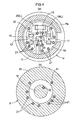
The substrate P comprises a non-conductive substrate base Pa
formed of e.g. glass epoxy. On each of the inner side (front side) and the
outer side (rear side) of this substrate base Pa, there is provided a printed
circuit formed in a predetermined pattern by e.g. etching of a good
conductor such as a copper foil, as illustrated in Figs. 3 and 4. More
particularly, as shown in Fig. 4 (b), on the outer side of the substrate P,
there are formed an annular outer contact portion 15 which contacts when
the lateral wall 3 of the case C is folded inwards and an output portion 16
located at the center position. Further, as shown in Fig. 3 and Fig. 4 (a),
on the inner side of the substrate P, there are formed an annular inner
contact portion 17 which comes into contact with the conductive ring 7 and
an annular ground 18 located within the inner contact portion 17. In
addition, within this ground 18, there are formed a first conductive portion
19 and a second conductive portion 20 independently of each other.
Further, the ground 18 is electrically coupled to the outer contact portion 15
through a plurality of through holes 21. The first conductive portion 19
and the second conductive portion 20 form a signal line L and the second
conductive portion 20 is electrically coupled to the output portion 16 via the
through holes 22.
As shown in Fig. 4, at the center position of the inner side of the
substrate P and mounted on the ground 18, the MOS type and
enhancement type FET 10 is fixed there by means of an adhesive agent.
And, a gate terminal G of this FET 10 and its projecting portions to be
electrically coupled to the inner contact portion 17 are bonded together by
means of bonding wires 23 respectively. Further, a chip type capacitor 11
is conductively interposed between the first conductive portion 19 and the
ground 19, a chip type varistor 12 is conductively interposed between the
second conductive portion 20 and the ground 18, and a chip type resistor 13
is conductively interposed between the first conductive portion 19 and the
second conductive portion 20. Incidentally, the chip capacitor 11, the chip
varistor 12 and the chip resistor 13 are first mounted at the
above-described respective mounting positions by means of cream solder
and then fixed under the soldered condition through a reflow processing.
The chip type capacitor 11 employed comprises one having a
capacitance suitable for noise rejection (e.g. which provides the lowest
impedance at the particular frequency used by the GMS system). The chip
varistor 12 employed comprises one whose varistor voltage has a value
slightly higher than a voltage to be impinged between a drain terminal D
and a source terminal S of the FET 10. The chip resistor 13 employed
comprises one having a resistance value suitable for noise rejection.
For assembling this electret condenser microphone, first, the
spacer 4, the diaphragm 6 supported to the support ring 5 and the
conductive ring 7 will be fitted inside the case C having the electret portion
E formed in the manner described above. Next, the substrate P mounting
thereon the FET 10, the chip capacitor 11, the chip varistor 12 and the chip
resistor 13 will be fitted into the rear end opening of the case C.
Thereafter, in order to permanently fix the substrate P to the case C, a
reducing operation will be effected for bending inward the ends of the
lateral wall 3 of the case C. When this assembly operation is completed, a
spacing (of e.g. 25 µm) equal to the thickness (d) of the spacer 4 is formed
between the front-end wall 2 and the diaphragm 6 and also the film coating
F formed on the inner side of the lateral wall 3 of the case C electrically
insulates the outer peripheral face of the conductive ring 7 from the lateral
wall 3 of the case C. With this electret condenser microphone completed in
the manner described above, the inner contact portion 17 formed on the
inner side of the substrate P contacts the conductive ring 7 thereby to
establish electrical connection therebetween, and also the outer contact
portion 15 formed on the outer side of the substrate P contacts the lateral
wall 3 of the case C thereby to establish electric connection therebetween.
Hence, an electric conduction is established between these components and
the circuit on the substrate, so that a variation in capacitance developed
between the front-end face 2 of the case C and the diaphragm 6 can be
obtained and outputted as an electric signal from the output portion 16.
Incidentally, the electric circuit of this electret condenser
microphone can be diagrammatically represented as illustrated in Fig. 5.
In this figure, in case the N channel MOS FET 10 is employed, "input"
corresponds to the gate G, "output" corresponds to the drain D and "ground"
corresponds to the source S, respectively.
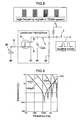
Fig. 6 graphically shows results of measurements on noises
(represented as detection levels) appearing on the signal line L under an
environment affected by high-frequency noise in comparison between the
electret condenser microphone of the invention having the above-described
construction and the conventional electret condenser microphone
(conventional product) such as the one shown in Fig. 8. As may be clearly
seen in this figure, in the case of the conventional electret condenser
microphone (conventional product), a high detection level is maintained up
to about 100 MHz, the detection level then decreases at frequencies higher
than about 100 MHz and the detection level decreases most significantly at
900 MHz which corresponds to the frequency employed by the GSM system.
On the other hand, in the case of the electret condenser microphone
according to the present invention (improved product), the detection level is
lower as a whole. And, the detection level decreases as the frequency rises
to about 60 MHz. And, the detection level is maintained still low even in
the frequency range higher than the frequency of 60 MHz.
In this way, with the electret condenser microphone relating to the
present invention, as this microphone includes the MOS FET 10, the
capacitor 11, the varistor 12 and the resistor 13 mounted on the substrate P,
even when an external noise is applied to the signal line L, the impedance
is reduced due to the self-resonance of the capacitor 11, so that this noise is
eliminated by being drained to the ground 18. Further, when the voltage
of the signal line L is raised by the effect of this noise, as the resistance
value of the varistor 12 is reduced for nose in broad band, the noise on the
signal line L can be rejected again by being drained to the ground 18. In
addition, the resistor 13 provides the function of lowering the level of signal
flowing in the signal line L. Also, with this electret condenser microphone,
the electro-acoustic transducer M, the MOS FET 10, the capacitor 11, the
varistor 12 and the resistor 13 are all accommodated under the shielded
condition thereof inside the capsule C and moreover, on the substrate P, the
MOS FET 10, the capacitor 11, the varistor 12, the resistor 13 and the
signal line L are all disposed within its surface area surrounded by the
ground 18. Hence, the level of such external noise can be reduced
significantly.
With the provision of the above-described construction, when this
microphone is employed in a frequency-switchover type mobile telephone
such as one implementing the dual-band system, high frequency noise due
to the two frequencies can be rejected effectively. In addition, even when
the microphone is subjected to a nose in the audible frequency range as in
the TDMA system, the MOS type FET 10 designed for audio use can reject
such noise which generates an annoying audible sound. In this way, the
microphone can reduce not only noise of high frequency, by also nose of
broad band including audible frequencies.
In particular, as compared with the junction FET, the MOS FET
10 provides a higher impedance between the drain terminal D and the
source terminal S. Hence, only a very small amount of current flows even
when a voltage is impinged thereto. So that, there occurs no wasteful
power consumption. Specifically, the power consumption can be reduced to
1/3 approximately. Moreover, the standard MOS type FET 10 provides a
high heat resistance as high as up to about 130°C. This enables its use in a
high-temperature environment such as in an engine room of an automobile.
[Other Embodiment]
In addition to the foregoing embodiment, the present invention can
be embodied by providing the characterizing features of the invention in an
electret condenser microphone having such constructions as described next.
In the following discussion of the further embodiment, the components
having substantially same functions as those in the foregoing embodiment
will be denoted and described with same reference numerals and marks as
the foregoing embodiment.
Needless to say, in any one of the three kinds of electret condenser
microphones relating to this further embodiment, it is possible to embody
the invention by implementing the substrate P having the printed circuit
described in the foregoing embodiment and/or implementing the
construction in which the entire circuit construction is accommodated
within a metal capsule C. Therefore, the above-described functions and
effects of the present invention can be achieved fully also when the
invention is embodied in any one of the three kinds of modes described in
this further embodiment.
Industrial Applicability
The electret condenser microphone relating to the present
invention consumes only small power and can reject noise over broad band.
Hence this microphone can be suitably used as a microphone in a mobile
telephone. Further, as this electret condenser microphone can be used
even under a high-temperature environment, this can be suitably used also
as e.g. a sensor to be disposed inside an engine room of an automobile.