EP1473619A1 - Multiple clocks with superperiod - Google Patents
Multiple clocks with superperiod Download PDFInfo
- Publication number
- EP1473619A1 EP1473619A1 EP03101192A EP03101192A EP1473619A1 EP 1473619 A1 EP1473619 A1 EP 1473619A1 EP 03101192 A EP03101192 A EP 03101192A EP 03101192 A EP03101192 A EP 03101192A EP 1473619 A1 EP1473619 A1 EP 1473619A1
- Authority
- EP
- European Patent Office
- Prior art keywords
- signal
- superperiod
- clock
- clock signal
- signals
- Prior art date
- Legal status (The legal status is an assumption and is not a legal conclusion. Google has not performed a legal analysis and makes no representation as to the accuracy of the status listed.)
- Granted
Links
Images


Classifications
-
- G—PHYSICS
- G06—COMPUTING; CALCULATING OR COUNTING
- G06F—ELECTRIC DIGITAL DATA PROCESSING
- G06F1/00—Details not covered by groups G06F3/00 - G06F13/00 and G06F21/00
- G06F1/04—Generating or distributing clock signals or signals derived directly therefrom
- G06F1/06—Clock generators producing several clock signals
Definitions
- the present invention relates to the synchronization of a multitude of clock signals, and to establishing well-defined phase relations between said clock signals.
- the apparatus comprises a set of clock signal circuits that generate m clock signals of at least two different clock frequencies, whereby m is a natural number. Furthermore, the apparatus comprises a superperiod signal-generating unit that derives a first superperiod signal from a dedicated clock signal of said set of clock signals. The signal period of the first superperiod signal, the "superperiod", is a common multiple of the clock signals' signal periods.
- the m clock signals might have random phase relations relative to each other, whereby the respective phase relation might e.g. depend on the initial conditions when starting the system's clock generators.
- the invention provides a first superperiod signal, which is a clock signal with a rather long signal period.
- One signal period of said first superperiod signal is a common multiple of each of the clock signals' signal periods. For example, in case there is a first clock signal with a signal period of 2 ns and a second clock signal with a signal period of 3 ns, then the superperiod might be chosen as 6 ns, 12 ns, 18 ns, etc.
- the first superperiod signal When said first superperiod signal is synchronous with a respective clock signal, then the edges of the first superperiod signal coincide with at least some of the edges of the clock signal.
- the first superperiod signal can be understood as an auxiliary means for analyzing the phase relations of the various clock signals, because it allows to monitor if a respective clock signal is in phase with said first superperiod signal or not. If several clock signals are in phase with the first superperiod signal, then these clock signals are in phase with each other, too.
- the information obtained by analyzing the phase relations between said clock signals and the first superperiod signal may be used for synchronizing said clock signals to the first superperiod signal.
- one superperiod comprises n 1 signal periods of a first clock signal, and it comprises n 2 signal periods of a second clock signal, etc., whereby said clock signals may have different frequencies.
- one superperiod comprises n, signal periods of the i-th clock signal, whereby the n, are natural numbers, and whereby i ranges from 1 to m, with m being the total number of clock signals.
- the apparatus comprises synchronization means that synchronize at least some of the clock signals to said first superperiod signal.
- the synchronization facilities shift the phase of a respective clock signal in a way that a defined phase relation between said clock signal and said first superperiod signal is obtained.
- the random phase relations between the clock signals which e.g. have been caused by any transient effects when the clock generators start oscillating, are replaced by well-defined phase relations.
- the apparatus comprises a central facility that programs or reprograms the values n, corresponding to the i-th clock signal, with i ranging from 1 to m.
- the natural number n denotes the number of clock periods of the i-th clock signal within one superperiod. Reprogramming the number n, allows to vary the length of the superperiod and to generate any desired superperiod signal.
- said central facility may program or reprogram the clock frequency of the i-th clock signal, with 1 ⁇ i ⁇ m.
- the clock signal circuits might e.g. comprise programmable PLLs.
- the central facility might also have to reprogram one or more of the values n i, though this is not always necessary.
- any required set of clock frequencies can be provided.
- the lowest common multiple (LCM) of the clock signals' signal periods is chosen as the superperiod of the first superperiod signal.
- the natural numbers n are chosen as small as possible.
- the superperiod signal generating units are realized by means of counters, rather small counters can be used.
- Another advantage of using a rather short superperiod is that the time required for synchronizing the clock signals is kept small.
- the superperiod generating unit is realized by means of a first superperiod counter that counts at least one of the rising edges or the falling edges of the dedicated clock signal.
- the counter period of the first superperiod counter might e.g. be equal to n j , which means that one signal period of the first superperiod signal is generated per n j clock periods of said dedicated clock signal.
- the first superperiod counter might e.g. be realized as an upward counter or as a downward counter. In case the superperiod counter is implemented as an upward counter, the counter is reset as soon as the count (n j -1) is reached.
- the superperiod counter can be realized as a downward counter, with the value (n j -1) being reloaded when the count has reached zero.
- At least some of the clock signals are delayed until a subset of their edges coincide with edges of the first superperiod signal. Any one of the clock signals can be aligned to the first superperiod signal, which serves as a reference. By doing this, defined phase relations are established among the clock signals, though the clock signals have different frequencies.
- At least some of the clock signal circuits comprise variable delay elements adapted for phase shifting a respective clock signal until it is in phase with the first superperiod signal.
- first superperiod signal that has been derived from a dedicated clock signal has been used for the purpose of synchronization.
- second superperiod signals are derived from the other clock signals, and said second superperiod signals are synchronized to said first superperiod signal.
- the second superperiod signals have the same superperiod as the first superperiod signal, and for this reason, the determination of the second superperiod signal's phase relative to the first superperiod signal is simplified.
- both a respective clock signal and the corresponding second superperiod signal derived therefrom are delayed together, until the respective second superperiod signal is in phase with the first superperiod signal.
- a clock signal is subjected to a certain phase shift, then the second superperiod signal derived from said clock signal is automatically shifted by the same amount.
- said clock signal (and also the second superperiod signal derived therefrom) are delayed until the phase of the second superperiod signal is aligned with the phase of the first superperiod signal.
- the underlying clock signal is synchronized to said first superperiod signal.
- said second superperiod signals are derived from the respective clock signals by means of second superperiod counters.
- These second superperiod counters count at least one of the rising edges or the falling edges of the underlying i-th clock signal.
- a superperiod of the corresponding second superperiod signal might be generated for every n, signal periods of the i-th clock signal.
- the first superperiod signal is sampled in accordance with the i-the clock signal, and a series of sampling values is obtained. This series of sample values is monitored, and as soon as there is a signal transition, the corresponding second superperiod counter is initialized.
- the apparatus comprises phase detection units that determine the phase difference between the respective second superperiod signals and the first superperiod signal.
- phase detection units that determine the phase difference between the respective second superperiod signals and the first superperiod signal.
- Phase detection units can be implemented in a variety of different ways, for example by means of an XOR gate, a set/reset circuit, etc.
- said phase detection units are realized by means of flip-flops.
- the first superperiod signal is e.g. connected to the flip-flop's clock input, while the second superperiod signal is connected to the flip-flop's data input.
- a logical "1" is obtained at the flip-flop's output
- a logical "0" is obtained.
- the first superperiod signal might as well be applied to the flip-flop's data input, while the second superperiod signal might be connected to the flip-flop's clock input.
- the signal levels at the flip-flop's output are interchanged.
- the phase delay of the second superperiod signal might e.g. be varied until a transition of the flip-flop's output signal is observed. At the point where the transition occurs, said first and said second superperiod signal are synchronous to each other.
- the clock signal circuits comprise selection means that allow to select, besides the respective clock signal circuit's own clock signal, clock signals of remote clock signal circuits as an output signal.
- a clock signal circuit can simultaneously provide clock signals of different clock frequencies to the circuits connected therewith.
- the clock signal circuits might be linked in order to form a ring of clock signal circuits, whereby on each of the clock signal circuits, both the own clock signal and a clock signal of a preceding clock signal circuit are available.
- any clock signal of said set of m clock signals may be selected as the dedicated clock signal from which the first superperiod signal is derived.
- Any of the clock signal circuits may generate the first superperiod signal, which is distributed as a reference signal to the other clock signal circuits.
- a clock signal circuit having two modes of operation can be employed. In the first mode of operation, the clock signal circuit generates a first superperiod signal that is distributed to the other clock signal circuits. In the second mode of operation, the clock signal circuit synchronizes its own clock signal to a superperiod signal that is generated on the part of a remote clock signal circuit.
- the clock signals are utilized in a DUT testing environment.
- clock signals are required for providing stimulus signals to a DUT, or for receiving response signals from a DUT, or for both of these purposes.
- SOCs Systems on a Chip
- a multitude of different clock frequencies might be required, because chips of this kind often comprise a multitude of different clock domains.
- a first DUT core has to be addressed with a first clock frequency, while for a second DUT core, another clock frequency is required.
- Test sequences do not only test one DUT core at a time. There exist test sequences where two or more DUT cores are involved simultaneously, in order to check the interplay between different DUT cores.
- the clock signals that are required for simultaneously accessing DUT cores of different clock domains must have well-defined phase relations relative to each other, because otherwise, faulty test results might be obtained. Random phase relations between the clock signals may cause unpredictable results.
- the required set of synchronized clock signals of different clock frequencies can be provided by embodiments of the present invention.
- Embodiments of the invention might be used in an automated test equipment (ATE), use of the invention is not restricted to this application.
- Embodiments of the present invention might e.g. be utilized in any kind of data processing system where clock signals of different clock frequencies are required.
- a processing unit might be operated at a rather high clock frequency, while a much lower clock frequency is required for a bus system that cooperates with said processing unit.
- a phase alignment of the respective clock signals as described above will possibly improve the reliability of data exchange between these functional units.
- the invention can be partly or entirely embodied or supported by one or more suitable software programs, which can be stored on or otherwise provided by any kind of data carrier, and which might be executed in or by any suitable data processing unit.
- Software programs or routines are preferably applied for programming and reprogramming at least one of: the values n i, the clock signal's frequencies, and the delays of the variable delay elements.
- the present invention can be utilized whenever a multitude of clock signals of different clock frequencies is required, with said clock signals having well-defined phase relations relative to each other.
- the invention will be described with respect to an application in the field of testing. However, the invention is in no way restricted to the field of testing, but can be used in other fields as well.
- the present invention might be employed for providing a complex system with a plurality of different clock frequencies having well-defined phase relations relative to each other.
- FIG. 1 a typical test environment is shown.
- a DUT (Device Under Test) 1 is connected to an ATE (Automated Test Equipment) 2.
- ATE Automatic Test Equipment
- the DUT 1 is exposed to various types of stimulus signals generated by the ATE 2, and the responses of the DUT 1 are measured and processed. Usually, the response signals are compared to an expected response of a good device.
- the DUT 1 might for example be an integrated circuit. Because of the ever-increasing integration of capabilities on a single integrated circuit, the DUT 1 might comprise various different functional units, such as e.g. random access memories, read-only memories, microprocessor units, digital signal processors, local area network modules, etc.
- the term "DUT-core" will be used for generally representing an architectural component within a DUT.
- a DUT-core is characterized by a behavioral model, signal timing conditions, and by an interface specified in terms of a set of input and output signals.
- the DUT 1 shown in Fig. 1 comprises two DUT-cores 3 and 4, whereby each of said DUT-cores represents one or more functional units of the DUT.
- the DUT-cores 3, 4 might be analogous, digital, or memory DUT-cores.
- the DUT-core 3 is accessible through the DUT-pins 5a, 5b,...5e, and similarly, the DUT-core 4 can be accessed through the DUT-pins 6a, 6b,...6f.
- the automated test equipment 2 shown in Fig. 1 is based on a per-pin architecture, which means that for each of the DUT-pins 5a, 5b,...5e, there exists a corresponding per-pin testing unit 7a, 7b,...7e.
- a dedicated per-pin testing unit 8a,8b,...8f for each of the DUT-pins 6a, 6b,...6f, there is a dedicated per-pin testing unit 8a,8b,...8f.
- Each DUT-pin of the DUT 1 can be addressed by a corresponding decentralized per-pin testing unit of the ATE 2.
- the per-pin architecture generally enables high performance and scalability at acceptable costs.
- Examples for automated test equipments with a per-pin architecture are the Agilent 83000 and 93000 families of Semiconductor Test Systems of Agilent Technologies. Details of those families are disclosed e.g. in EP-A-859318, EP-A-864977, EP-A-886214, EP-A-882991, US-A-5,499,248, US-A-5,453,995.
- the invention is not restricted to ATEs with per-pin architectures, but might as well be used in an ATE with centralized resources.
- One or more per-pin testing units together constitute a so-called ATE-port, which is an independent testing unit within the ATE.
- the DUT-core 3 is accessed by the ATE-port 9, which comprises the per-pin testing units 7a,7b,...7e.
- the DUT-core 4 is accessed by the ATE-port 10, which comprises the per-pin testing units 8a, 8b,...8f.
- Each ATE-port is assigned to a corresponding DUT-core and performs a test of the respective DUT-core. Since the ATE-ports represent independent functional units within the ATE, the testing of the addressed DUT-cores in the DUT can be provided not only serially, i.e. the DUT-cores are tested successively, but also in parallel, i.e. more than one DUT-core will be tested concurrently.
- the DUT-cores 3, 4 might be analogous, digital, or memory DUT-cores, and they might belong to different clock domains. Therefore, a variety of clock signals with different clock frequencies might be required, in order to provide the DUT with stimulus signals, and in order to receive response signals from the DUT.
- a test sequence involves two or more DUT-cores that belong to different clock domains, there might be a data exchange between the various DUT-cores.
- the clock signals generated by the ATE are used for clocking data into a respective DUT-core, and for receiving data from a respective DUT-core.
- the obtained test results might depend on said random phase relations. For this reason, random phase relations can cause non-predictable test results. It is therefore required that the various clock signals provided by the ATE have well-defined phase relations relative to each other.
- Fig. 2 shows a system of clock boards for generating multiple clock signals of various different clock frequencies, whereby said clock signals have well-defined phase relations relative to each other.
- a system of clock boards can be employed in an ATE, but it can also be employed in other fields.
- the system comprises a first clock board 11 that generates a clock signal of a first frequency, and a second clock board 12 that generates a clock signal of a second frequency.
- the system shown in Fig. 2 might further comprise additional clock boards for generating further clock signals.
- Each of the clock boards comprises a phase locked loop (PLL) circuit adapted for generating the respective clock signal.
- a low-frequency reference clock signal 13 of e.g. 10 MHz is provided to the PLL 14 of the first clock board 11, to the PLL 15 of the second clock board 12, and to the PLLs of the other clock boards.
- the PLL 14 Starting from the reference clock signal 13, the PLL 14 generates a first clock signal 16 with a clock frequency of e.g. 500 MHz, which corresponds to a signal period of 2 ns.
- the PLL 14 might be a programmable PLL, whereby the clock frequency of the PLL 14 can be set by means of a frequency programming signal 17.
- Said frequency programming signal 17 is provided by a control unit 18 located on the first clock board 11.
- the first clock signal 16 is forwarded to a variable delay unit 19.
- the delay of said delay unit 19 is specified by a delay control signal 20 that is also generated by the control unit 18.
- the delay of the variable delay unit 19 is set to a constant.
- a delayed first clock signal 21 of 500 MHz is obtained at the output of the variable delay unit 19, and said clock signal is provided to the circuits of the 500 MHz clock domain.
- the PLL 15 on the second clock board 12 generates a second clock signal 22.
- the frequency-programming signal 23 is obtained from a control unit 24 located on the second clock board 12.
- a central control facility (not shown) might forward control signals 25 to the control units 18, 24, e.g. in order to indicate the required clock frequencies.
- the clock frequency of the second clock signal 22 has been set to 200 MHz, which corresponds to a signal period of 5 ns.
- the second clock signal 22 is delayed by a variable delay unit 27.
- the delay of the variable delay unit 27 is adjusted according to a delay control signal 28 that might be obtained from the control unit 24 as well.
- a delayed second clock signal 29 of 200 MHz is obtained, and said clock signal is provided to the circuits of the 200 MHz clock domain.
- the next task is to synchronize the system's different clock signals, and to establish well-defined phase relations between clock signals of different frequencies.
- a superperiod signal is derived from at least one of the system's clock signals, with the signal period of said superperiod signal being a common multiple of all the clock signals' signal periods.
- One possibility is to choose the lowest common multiple (LCM) of all the signal periods within the system as a superperiod. Any other common multiple of the clock signals' signal periods might be used as well.
- the signal period of the superperiod signal should not become too large, though.
- the first clock signal 16 has a signal period of 2 ns
- the second clock signal 22 has a signal period of 5 ns.
- the signal period of the superperiod signal can therefore be chosen as 10 ns (which is the lowest common multiple, LCM, of 2 ns and 5 ns), or as 20 ns, 30 ns, etc.
- a superperiod signal with a superperiod of 10 ns is generated by means of a superperiod counter. For each of the clock signals' signal periods, there exists a corresponding natural number by which the respective signal period has to be multiplied in order to obtain one superperiod.
- the signal period 2 ns of the 500 MHz clock signal has to be multiplied by five in order to obtain a superperiod of 10 ns.
- the 5 ns signal period of the second clock board's 200 MHz clock signal has to be multiplied by two.
- n shall denote the respective natural number by which the signal period of the i-th clock signal has to be multiplied in order to obtain the superperiod signal's signal period.
- the delayed first clock signal 21 of the first clock board 11 is input to a superperiod counter 30.
- a superperiod signal W_SP is obtained.
- Per n 1 5 clock cycles of the superperiod counter's input signal, one superperiod of the superperiod signal W_SP is generated.
- the superperiod counter 30 either counts the rising edges or the falling edges of the delayed first clock signal 21.
- the superperiod counter 30 might be implemented as an upward counter or as a downward counter. In case it is realized as an upward counter, the count is reset to zero as soon as the maximum count (n 1 -1) is reached. In case the superperiod counter is realized as a downward counter, the value n 1 -1 is reloaded each time the count has reached zero.
- the superperiod counter 30 might be implemented as a programmable counter, which means that the value n 1 can be set to any desired value.
- the value n 1 denotes the number of periods of the first clock signal per superperiod.
- the control unit 18 might provide a superperiod programming signal 31 to the superperiod counter 30.
- the delayed first clock signal 21 and the superperiod signal W_SP are depicted as a function of time.
- the respective counts are indicated underneath the delayed first clock signal 21.
- the count is equal to zero
- the superperiod signal W_SP is equal to zero as well.
- the superperiod signal W_SP generated by the first clock board 11 is distributed to all the other clock boards of the system, e.g. to the second clock board 12.
- the superperiod signal W_SP will further on be referred to as the "wiring board superperiod signal”.
- the second clock board 12 comprises a superperiod counter 35 that generates, from the delayed second clock signal 29, a local superperiod signal L_SP with a superperiod of 10 ns.
- the superperiod counter might be implemented as an upward counter.
- the superperiod counter 35 might be realized as a programmable counter, whereby the counter period n 2 can be set to any desired value.
- the counter period n 2 might be programmed or reprogrammed by means of a counter period programming signal 36 that is provided by the control unit 24.
- control unit 18 may set both the frequency of the PLL 14 and the counter period n 1 of the superperiod counter 30.
- the control unit 24 may set the frequency of the PLL 15, the delay of the variable delay unit 27, and the counter period n 2 of the superperiod counter 35. This allows to set the clock frequencies to any desired frequency, and to adapt the natural numbers n 1 and n 2 in a way that the respective superperiods of the superperiod signals W_SP and L_SP are equal to each other.
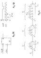
- Fig. 3B an alternative way of generating the superperiod signals W_SP and L_SP is shown.
- the delayed first clock signal 21, the superperiod signal W_SP, the delayed second clock signal 29 and the superperiod signal L_SP are depicted as a function of time.
- the respective counter values of the superperiod counter 30 are depicted underneath the delayed first clock signal 21.
- the embodiment of Fig. 3B allows to generate a superperiod signal W_SP with a duty cycle of 1:2.
- Both the wiring board superperiod signal W_SP and the local superperiod signal L_SP are provided to a phase detector 37, and there, the phase of the local superperiod signal L_SP relative to the wiring board superperiod signal W_SP is determined.
- the phase detector 37 generates a phase compare signal 38 that indicates whether the local superperiod signal L_SP lags or leads in phase relative to the wiring board superperiod signal W_SP, which is used as a reference.
- a logic level "O" of the phase compare signal 38 might indicate a phase lead of L_SP relative to W_SP
- a logic level "1" of the phase compare signal 38 might indicate a phase lag of L_SP relative to W_SP.
- the phase compare signal 38 is forwarded to the control unit 24.
- the delay of the variable delay unit 27 is varied by the control unit 24.
- the aim is to modify the delay induced by the variable delay unit 27 in a way that a phase coincidence between the local superperiod signal L_SP and the wiri ng board superperiod signal W_SP is established.
- the delay control signal 28 has to be modified such that the delay of the variable delay unit 27 is reduced.
- the delay of the variable delay unit 27 has to be increased.
- the control unit 24 is responsible for generating a suitable delay control signal 28 in accordance with the phase compare signal 38.
- the phase detector 37 can be implemented in a variety of different ways, e.g. by means of XOR-gates, by means of set/reset circuits, etc.
- Fig. 4A shows how the phase detector 37 can be implemented by means of a flip-flop 39.
- the local superperiod signal L_SP is supplied to the clock input of the flip-flop 39, while the wiring board superperiod signal W_SP is forwarded to the flip-flop's data input D.
- the superperiod signal W_SP at the data input D is sampled according to the superperiod signal L_SP. Each time a rising edge of the superperiod signal L_SP occurs, the value of the signal W_SP is captured.
- the obtained sample values are provided, as a phase compare signal Q, at the flip-flops's output.
- the superperiod signals W_SP and L_SP are shown as a function of time, together with the output signal Q.
- the rising edge 40 of L_SP precedes the rising edge 41 of W_SP.
- L_SP is provided to the flip-flop's clock input, W_SP is sampled at the instant of time defined by the rising edge 40.
- the signal level of W_SP is equal to "0", and the output signal Q will be equal to "0" as well. This means that the delay of the variable delay unit 27 has to be increased.
- Fig. 4C a different situation is shown in which there is a phase lag of L_SP relative to W_SP.
- the rising edge 42 of W_SP precedes the rising edge 43 of L_SP.
- the superperiod signal W_SP is sampled at the point of time defined by the rising edge 43, and the signal level "1" appears at the flip-flop's output.
- a signal level "1" of the phase compare signal Q indicates that the delay of the variable delay unit 27 has to be decreased.
- the superperiod counter 35 When the superperiod counter 35 starts counting at an arbitrary point of time, the local superperiod signal L_SP will have an arbitrary phase delay relative to the signal W_SP, and in order to compensate said phase delay, the variable delay unit might have to be set to a rather large delay value. In order to restrict the required delay to small values, it is suggested to initialize the superperiod counter 35 in dependence on a signal transition of the wiring board superperiod signal W_SP.
- Fig. 5A shows a circuit that can be used for determining the instant of time at which the superperiod counter should be reset or initialized.
- the circuit comprises a flip-flop 44, whereby the i-th clock signal is applied to the flip-flop's clock input, and whereby the wiring board superperiod signal W_SP is applied to the flip-flop's data input. With each rising edge of the i-th clock signal, a sampling value of the wiring board superperiod signal W_SP is obtained. The respective sampling values of W_SP are provided as an output signal of the flip-flop 44.
- Fig. 5B shows the superperiod signal W_SP, the i-th clock signal, and the flip-flop's output signal as a function of time.
- a corresponding sample value of W_SP is obtained.
- the rising edge 45 precedes the signal transition 48 of W_SP, and the sample value "0" is obtained.
- the signal transition 48 of W_SP has already taken place, and therefore, the sample value "1" is obtained.
- the signal transition of W_SP can be detected.
- the superperiod counter is initialized (49).
- the count of the superperiod counter has to be incremented by one (in case an upward counter is used) or decremented by one (in case a downward counter is employed) in order to compensate for the missing clock cycle.
- the superperiod counter is realized as an upward counter, the counter is set to +1.
- the superperiod counter is realized as a downward counter, the value (n,-2) is loaded into the counter.
- Fig. 6 shows how the variable delay units 19, 27 can be implemented as digital delay units.
- the digital delay unit of Fig. 6 comprises three stages 50, 51, 52.
- the upper branch 53 of the first stage 50 comprises one delay element 54, while the lower branch 55 of the first stage 50 comprises no delay elements at all.
- the multiplexer 56 it is possible to select either the delayed signal of the upper branch 53 or the non-delayed signal of the lower branch 55 as an output signal of the first stage 50.
- the upper branch 57 comprises two delay elements 58, and the lower branch 59 does not comprise any delay elements.
- the multiplexer 60 allows to select either the signal of the upper branch 57 or the signal of the lower branch 59 as an output signal.
- the third stage 52 comprises an upper branch 61 with four delay elements 62, and a lower branch 63 without any delay elements.
- the multiplexers 56, 60, 64 By programming the multiplexers 56, 60, 64 accordingly, any desired number of delay elements between zero and seven can be included in the signal path.
- the desired delay might be programmed by means of a bit pattern, whereby the least significant bit (LSB) of the bit pattern is provided to the multiplexer 56, and whereby the most significant bit (MSB) of the bit pattern is provided to the multiplexer 64.
- LSB least significant bit
- MSB most significant bit
- the multiplexer 64 might be switched from the lower branch 63 to the upper branch 61 immediately after an edge of a respective signal has reached the multiplexer 64. In this case, one might obtain two pulses (instead of one) at the multiplexer's output.
- a solution to these problems is provided by the following procedure: Whenever the delay has to be reprogrammed, the switch 66 at the input of the variable delay unit is opened for k clock periods, with k being a natural number. Then, the respective multiplexers are reprogrammed, and then, the switch 66 is closed. Now, k clock cycles have been omitted, and therefore, the count of the respective superperiod counter has to be incremented (in case an upward counter is used) or decremented (in case a downward counter is employed) by k, in order to compensate for the missing clock cycles.
- variable delay units 19, 27 might be implemented as analogue delay units, whereby the delay of said analogue delay units may be set by an analogue control signal.
- Fig. 7 shows a set of clock boards for generating a plurality of clock signals for an automated test equipment (ATE).
- ATE automated test equipment
- a first clock generator 68 generates a first clock signal 69
- a second clock generator 71 generates a second clock signal 72.
- Both the first and the second clock generators 68, 71 are provided with a reference clock signal 73.
- the system's various clock boards are connected in order to form a ring structure.
- the first clock board 67 receives a clock signal 74 from a preceding clock board.
- the multiplexer 75 allows to select either the clock signal 74 from the preceding clock board or the first clock signal 69 from the first clock board 67.
- the selected clock signal is forwarded, as a clock signal 76, to the second clock board 70.
- the multiplexer 77 on the second clock board is provided with the second clock signal 72 and with said clock signal 76.
- the multiplexer 77 selects one of said two clock signals as a clock signal 78, and said clock signal 78 is forwarded to the subsequent clock board of the ring structure.
- clock signals are passed from one clock board to a subsequent clock board.
- the last one of the sequence of clock boards will provide the clock signal 74 to the first clock board 67.
- a test equipment comprises a set of card cages, whereby a card cage typically comprises one clock board and e.g. eight channel boards. Dependent on the respective embodiment, there might exist 16, 32 or even 64 channels per channel board. Said channels provide stimulus signals to a DUT and receive response signals from the DUT.
- Each of the clock boards 67, 70 shown in Fig. 7 has to provide clock signals to e.g. eight different channel boards.
- the first clock board 67 comprises eight multiplexers 79a, 79b,..., whereby each of said multiplexers is assigned to a corresponding channel board.
- the multiplexer 79a permits to select either the first clock signal 69 or the clock signal 74 as a channel clock signal 80a for the first channel board.
- the multiplexer 79b allows to choose one of the two clock signals 69, 74 as a channel clock signal 80b for the second channel board, etc.
- each of the channel boards can be individually provided with a selected channel clock signal.
- the second cock board 70 also has to provide channel clock signals for eight different channel boards.
- the second clock board comprises eight multiplexers 83a, ..., whereby each of said multiplexers allows to select either the second clock signal 72 or the clock signal 76 as a corresponding channel clock signal 84a, ....
- a so-called switch fabric might be used for exchanging clock signals between the various clock boards.
Abstract
Description
- The present invention relates to the synchronization of a multitude of clock signals, and to establishing well-defined phase relations between said clock signals.
- When there exist clock domains with different clock frequencies within a system, data transfer or data exchange between said clock domains might lead to unpredictable results. Transient effects when the system's different clock generators are started are the cause of a random phase relation between the system's different clock signals. Therefore, when data is sent from the domain of a first clock signal to a second clock signal's domain, unpredictable results may occur that are caused by the random phase relations between the different clock signals.
- It is an object of the invention to provide an improved generation of multiple clock signals. The object is solved by the independent claims. Preferred embodiments are shown by the dependent claims.
- The apparatus according to the invention comprises a set of clock signal circuits that generate m clock signals of at least two different clock frequencies, whereby m is a natural number. Furthermore, the apparatus comprises a superperiod signal-generating unit that derives a first superperiod signal from a dedicated clock signal of said set of clock signals. The signal period of the first superperiod signal, the "superperiod", is a common multiple of the clock signals' signal periods.
- Initially, the m clock signals might have random phase relations relative to each other, whereby the respective phase relation might e.g. depend on the initial conditions when starting the system's clock generators. In order to monitor the phase relations between the different clock signals, the invention provides a first superperiod signal, which is a clock signal with a rather long signal period. One signal period of said first superperiod signal is a common multiple of each of the clock signals' signal periods. For example, in case there is a first clock signal with a signal period of 2 ns and a second clock signal with a signal period of 3 ns, then the superperiod might be chosen as 6 ns, 12 ns, 18 ns, etc. When said first superperiod signal is synchronous with a respective clock signal, then the edges of the first superperiod signal coincide with at least some of the edges of the clock signal. For this reason, the first superperiod signal can be understood as an auxiliary means for analyzing the phase relations of the various clock signals, because it allows to monitor if a respective clock signal is in phase with said first superperiod signal or not. If several clock signals are in phase with the first superperiod signal, then these clock signals are in phase with each other, too.
- Optionally, the information obtained by analyzing the phase relations between said clock signals and the first superperiod signal may be used for synchronizing said clock signals to the first superperiod signal. When several clock signals are in phase with the first superperiod signal, this implies that they are in phase with each other as well. This allows establishing well-defined phase relations between clock signals of different frequencies.
- The feature that the signal period of the first superperiod signal is a common multiple of the clock signals' signal periods can alternatively be expressed as follows: one superperiod comprises n1 signal periods of a first clock signal, and it comprises n2 signal periods of a second clock signal, etc., whereby said clock signals may have different frequencies. Generally speaking, one superperiod comprises n, signal periods of the i-th clock signal, whereby the n, are natural numbers, and whereby i ranges from 1 to m, with m being the total number of clock signals.
- According to a preferred embodiment of the invention, the apparatus comprises synchronization means that synchronize at least some of the clock signals to said first superperiod signal. The synchronization facilities shift the phase of a respective clock signal in a way that a defined phase relation between said clock signal and said first superperiod signal is obtained. The random phase relations between the clock signals, which e.g. have been caused by any transient effects when the clock generators start oscillating, are replaced by well-defined phase relations.
- In another embodiment, the apparatus comprises a central facility that programs or reprograms the values n, corresponding to the i-th clock signal, with i ranging from 1 to m. The natural number n, denotes the number of clock periods of the i-th clock signal within one superperiod. Reprogramming the number n, allows to vary the length of the superperiod and to generate any desired superperiod signal.
- According to another preferred embodiment of the invention, said central facility may program or reprogram the clock frequency of the i-th clock signal, with 1 ≤ i ≤ m. By programming or reprogramming at least one of the clock generators of the respective clock signal circuits, any required set of clock frequencies can be generated. The clock signal circuits might e.g. comprise programmable PLLs. In order to adapt the superperiod of the first superperiod signal to the modified clock frequencies, the central facility might also have to reprogram one or more of the values ni, though this is not always necessary. By means of programmable clock generators and programmable superperiod signal generating units, any required set of clock frequencies can be provided.
- According to a preferred embodiment of the invention, the lowest common multiple (LCM) of the clock signals' signal periods is chosen as the superperiod of the first superperiod signal. In this embodiment, the natural numbers n, are chosen as small as possible. In case the superperiod signal generating units are realized by means of counters, rather small counters can be used. Another advantage of using a rather short superperiod is that the time required for synchronizing the clock signals is kept small.
- In a preferred embodiment, the superperiod generating unit is realized by means of a first superperiod counter that counts at least one of the rising edges or the falling edges of the dedicated clock signal. The counter period of the first superperiod counter might e.g. be equal to nj, which means that one signal period of the first superperiod signal is generated per nj clock periods of said dedicated clock signal. The first superperiod counter might e.g. be realized as an upward counter or as a downward counter. In case the superperiod counter is implemented as an upward counter, the counter is reset as soon as the count (nj-1) is reached. Alternatively, the superperiod counter can be realized as a downward counter, with the value (nj-1) being reloaded when the count has reached zero.
- According to a further preferred embodiment of the invention, at least some of the clock signals are delayed until a subset of their edges coincide with edges of the first superperiod signal. Any one of the clock signals can be aligned to the first superperiod signal, which serves as a reference. By doing this, defined phase relations are established among the clock signals, though the clock signals have different frequencies.
- Preferably, at least some of the clock signal circuits comprise variable delay elements adapted for phase shifting a respective clock signal until it is in phase with the first superperiod signal.
- So far, a first superperiod signal that has been derived from a dedicated clock signal has been used for the purpose of synchronization. According to a preferred embodiment of the invention, second superperiod signals are derived from the other clock signals, and said second superperiod signals are synchronized to said first superperiod signal. When the values ni are chosen appropriately, the second superperiod signals have the same superperiod as the first superperiod signal, and for this reason, the determination of the second superperiod signal's phase relative to the first superperiod signal is simplified.
- According to another preferred embodiment of the invention, both a respective clock signal and the corresponding second superperiod signal derived therefrom are delayed together, until the respective second superperiod signal is in phase with the first superperiod signal. When a clock signal is subjected to a certain phase shift, then the second superperiod signal derived from said clock signal is automatically shifted by the same amount. Now, said clock signal (and also the second superperiod signal derived therefrom) are delayed until the phase of the second superperiod signal is aligned with the phase of the first superperiod signal. As a result of this proceeding, also the underlying clock signal is synchronized to said first superperiod signal.
- According to another preferred embodiment of the invention, said second superperiod signals are derived from the respective clock signals by means of second superperiod counters. These second superperiod counters count at least one of the rising edges or the falling edges of the underlying i-th clock signal. For example, a superperiod of the corresponding second superperiod signal might be generated for every n, signal periods of the i-th clock signal.
- In case the second superperiod signals are generated by means of said second superperiod counters, the question arises when said counters should be started, in order to achieve that a respective second superperiod signal is not completely out of phase with said first superperiod signal. According to a preferred embodiment, the first superperiod signal is sampled in accordance with the i-the clock signal, and a series of sampling values is obtained. This series of sample values is monitored, and as soon as there is a signal transition, the corresponding second superperiod counter is initialized.
- By applying this initialization procedure, it can be achieved that the rising edge of the first superperiod signal is close to the rising edge of the second superperiod signal, though the two superperiod signals are not completely in phase yet. But now, starting from these pre-aligned signals, a rather small additional phase shift of the respective second superperiod signal will be sufficient to arrive at an exact alignment of the two superperiod signals, whereby the required additional phase shift is much smaller than a whole superperiod. The advantage of this initialization procedure is that a rather small variable delay is sufficient for synchronizing the first and the second superperiod signal. Furthermore, as the required additional phase shift is small, the synchronization will become more accurate.
- In a preferred embodiment of the invention, the apparatus comprises phase detection units that determine the phase difference between the respective second superperiod signals and the first superperiod signal. One might for example increase the phase shift of a respective second superperiod signal until the phase detection unit indicates that there is no phase delay between said first and said second superperiod signal any more.
- Phase detection units can be implemented in a variety of different ways, for example by means of an XOR gate, a set/reset circuit, etc. In a preferred embodiment of the invention, said phase detection units are realized by means of flip-flops. The first superperiod signal is e.g. connected to the flip-flop's clock input, while the second superperiod signal is connected to the flip-flop's data input. In case the second superperiod signal leads in phase relative to the first superperiod signal, a logical "1" is obtained at the flip-flop's output, and in case the second superperiod signal lags in phase relative to the first superperiod signal, a logical "0" is obtained. Alternatively, the first superperiod signal might as well be applied to the flip-flop's data input, while the second superperiod signal might be connected to the flip-flop's clock input. In this case, the signal levels at the flip-flop's output are interchanged.
- In order to synchronize the first and the second superperiod signal, the phase delay of the second superperiod signal might e.g. be varied until a transition of the flip-flop's output signal is observed. At the point where the transition occurs, said first and said second superperiod signal are synchronous to each other.
- According to a preferred embodiment of the invention, at least some of the clock signal circuits comprise selection means that allow to select, besides the respective clock signal circuit's own clock signal, clock signals of remote clock signal circuits as an output signal. Thus, a clock signal circuit can simultaneously provide clock signals of different clock frequencies to the circuits connected therewith. For example, the clock signal circuits might be linked in order to form a ring of clock signal circuits, whereby on each of the clock signal circuits, both the own clock signal and a clock signal of a preceding clock signal circuit are available.
- Preferably, any clock signal of said set of m clock signals may be selected as the dedicated clock signal from which the first superperiod signal is derived. Any of the clock signal circuits may generate the first superperiod signal, which is distributed as a reference signal to the other clock signal circuits. For example, a clock signal circuit having two modes of operation can be employed. In the first mode of operation, the clock signal circuit generates a first superperiod signal that is distributed to the other clock signal circuits. In the second mode of operation, the clock signal circuit synchronizes its own clock signal to a superperiod signal that is generated on the part of a remote clock signal circuit.
- According to a preferred embodiment of the invention, the clock signals are utilized in a DUT testing environment. In a testing environment, clock signals are required for providing stimulus signals to a DUT, or for receiving response signals from a DUT, or for both of these purposes. When testing more complicated chips, for example SOCs (Systems on a Chip), a multitude of different clock frequencies might be required, because chips of this kind often comprise a multitude of different clock domains. For example, a first DUT core has to be addressed with a first clock frequency, while for a second DUT core, another clock frequency is required.
- Test sequences do not only test one DUT core at a time. There exist test sequences where two or more DUT cores are involved simultaneously, in order to check the interplay between different DUT cores. The clock signals that are required for simultaneously accessing DUT cores of different clock domains must have well-defined phase relations relative to each other, because otherwise, faulty test results might be obtained. Random phase relations between the clock signals may cause unpredictable results. The required set of synchronized clock signals of different clock frequencies can be provided by embodiments of the present invention.
- Though embodiments of the invention might be used in an automated test equipment (ATE), use of the invention is not restricted to this application. Embodiments of the present invention might e.g. be utilized in any kind of data processing system where clock signals of different clock frequencies are required. For example, a processing unit might be operated at a rather high clock frequency, while a much lower clock frequency is required for a bus system that cooperates with said processing unit. A phase alignment of the respective clock signals as described above will possibly improve the reliability of data exchange between these functional units.
- The invention can be partly or entirely embodied or supported by one or more suitable software programs, which can be stored on or otherwise provided by any kind of data carrier, and which might be executed in or by any suitable data processing unit. Software programs or routines are preferably applied for programming and reprogramming at least one of: the values ni, the clock signal's frequencies, and the delays of the variable delay elements.
- Other objects and many of the attendant advantages of the present invention will be readily appreciated and become better understood by reference to the following detailed description when considering in connection with the accompanied drawings. Features that are substantially or functionally equal or similar will be referred to with the same reference sign(s).
- Fig. 1
- depicts an automated test environment (ATE) for testing a DUT;
- Fig. 2
- shows a system of clock boards for generating multiple clock signals of various different clock frequencies;
- Fig. 3
- shows two clock signals together with their corresponding superperiod signals as a function of time;
- Fig. 4
- shows a phase detection unit adapted for detecting the relative phase of the signals W_SP and L_SP;
- Fig. 5
- shows a circuit that can be used for initializing a superperiod counter;
- Fig. 6
- gives a circuit diagram of a digital delay unit; and
- Fig. 7
- shows how the system's clock boards can be connected to form a ring structure.
- The present invention can be utilized whenever a multitude of clock signals of different clock frequencies is required, with said clock signals having well-defined phase relations relative to each other. In the following, the invention will be described with respect to an application in the field of testing. However, the invention is in no way restricted to the field of testing, but can be used in other fields as well. For example, the present invention might be employed for providing a complex system with a plurality of different clock frequencies having well-defined phase relations relative to each other.
- In Fig. 1, a typical test environment is shown. A DUT (Device Under Test) 1 is connected to an ATE (Automated Test Equipment) 2. During a test, the
DUT 1 is exposed to various types of stimulus signals generated by the ATE 2, and the responses of theDUT 1 are measured and processed. Usually, the response signals are compared to an expected response of a good device. - The
DUT 1 might for example be an integrated circuit. Because of the ever-increasing integration of capabilities on a single integrated circuit, theDUT 1 might comprise various different functional units, such as e.g. random access memories, read-only memories, microprocessor units, digital signal processors, local area network modules, etc. In the following, the term "DUT-core" will be used for generally representing an architectural component within a DUT. A DUT-core is characterized by a behavioral model, signal timing conditions, and by an interface specified in terms of a set of input and output signals. - The
DUT 1 shown in Fig. 1 comprises two DUT-cores cores core 3 is accessible through the DUT-pins 5a, 5b,...5e, and similarly, the DUT-core 4 can be accessed through the DUT-pins 6a, 6b,...6f. - During test, at least some of the pins of the
DUT 1 are connected to the ATE 2. Theautomated test equipment 2 shown in Fig. 1 is based on a per-pin architecture, which means that for each of the DUT-pins 5a, 5b,...5e, there exists a corresponding per-pin testing unit pin testing unit DUT 1 can be addressed by a corresponding decentralized per-pin testing unit of the ATE 2. The per-pin architecture generally enables high performance and scalability at acceptable costs. Examples for automated test equipments with a per-pin architecture are the Agilent 83000 and 93000 families of Semiconductor Test Systems of Agilent Technologies. Details of those families are disclosed e.g. in EP-A-859318, EP-A-864977, EP-A-886214, EP-A-882991, US-A-5,499,248, US-A-5,453,995. The invention is not restricted to ATEs with per-pin architectures, but might as well be used in an ATE with centralized resources. - One or more per-pin testing units together constitute a so-called ATE-port, which is an independent testing unit within the ATE. The DUT-
core 3 is accessed by the ATE-port 9, which comprises the per-pin testing units core 4 is accessed by the ATE-port 10, which comprises the per-pin testing units - Each ATE-port is assigned to a corresponding DUT-core and performs a test of the respective DUT-core. Since the ATE-ports represent independent functional units within the ATE, the testing of the addressed DUT-cores in the DUT can be provided not only serially, i.e. the DUT-cores are tested successively, but also in parallel, i.e. more than one DUT-core will be tested concurrently.
- The DUT-
cores - Fig. 2 shows a system of clock boards for generating multiple clock signals of various different clock frequencies, whereby said clock signals have well-defined phase relations relative to each other. Such a system of clock boards can be employed in an ATE, but it can also be employed in other fields. The system comprises a
first clock board 11 that generates a clock signal of a first frequency, and a second clock board 12 that generates a clock signal of a second frequency. Besides that, the system shown in Fig. 2 might further comprise additional clock boards for generating further clock signals. Each of the clock boards comprises a phase locked loop (PLL) circuit adapted for generating the respective clock signal. A low-frequencyreference clock signal 13 of e.g. 10 MHz is provided to thePLL 14 of thefirst clock board 11, to thePLL 15 of the second clock board 12, and to the PLLs of the other clock boards. - Starting from the
reference clock signal 13, thePLL 14 generates afirst clock signal 16 with a clock frequency of e.g. 500 MHz, which corresponds to a signal period of 2 ns. In order to generate clock signals of any desired clock frequency, thePLL 14 might be a programmable PLL, whereby the clock frequency of thePLL 14 can be set by means of afrequency programming signal 17. Saidfrequency programming signal 17 is provided by acontrol unit 18 located on thefirst clock board 11. - The
first clock signal 16 is forwarded to avariable delay unit 19. The delay of saiddelay unit 19 is specified by adelay control signal 20 that is also generated by thecontrol unit 18. On thefirst clock board 11, the delay of thevariable delay unit 19 is set to a constant. A delayedfirst clock signal 21 of 500 MHz is obtained at the output of thevariable delay unit 19, and said clock signal is provided to the circuits of the 500 MHz clock domain. - The
PLL 15 on the second clock board 12 generates asecond clock signal 22. By means of the frequency-programming signal 23, the clock frequency generated by thePLL 15 can be varied within a certain range. The frequency-programming signal 23 is obtained from acontrol unit 24 located on the second clock board 12. A central control facility (not shown) might forward control signals 25 to thecontrol units - In the example of Fig. 2, it is assumed that the clock frequency of the
second clock signal 22 has been set to 200 MHz, which corresponds to a signal period of 5 ns. Thesecond clock signal 22 is delayed by avariable delay unit 27. The delay of thevariable delay unit 27 is adjusted according to adelay control signal 28 that might be obtained from thecontrol unit 24 as well. At the output of thevariable delay unit 27, a delayedsecond clock signal 29 of 200 MHz is obtained, and said clock signal is provided to the circuits of the 200 MHz clock domain. - The next task is to synchronize the system's different clock signals, and to establish well-defined phase relations between clock signals of different frequencies. For this purpose, a superperiod signal is derived from at least one of the system's clock signals, with the signal period of said superperiod signal being a common multiple of all the clock signals' signal periods. One possibility is to choose the lowest common multiple (LCM) of all the signal periods within the system as a superperiod. Any other common multiple of the clock signals' signal periods might be used as well. The signal period of the superperiod signal should not become too large, though.
- In our example, the
first clock signal 16 has a signal period of 2 ns, and thesecond clock signal 22 has a signal period of 5 ns. The signal period of the superperiod signal can therefore be chosen as 10 ns (which is the lowest common multiple, LCM, of 2 ns and 5 ns), or as 20 ns, 30 ns, etc. In our example, a superperiod signal with a superperiod of 10 ns is generated by means of a superperiod counter. For each of the clock signals' signal periods, there exists a corresponding natural number by which the respective signal period has to be multiplied in order to obtain one superperiod. For example, thesignal period 2 ns of the 500 MHz clock signal has to be multiplied by five in order to obtain a superperiod of 10 ns. Correspondingly, the 5 ns signal period of the second clock board's 200 MHz clock signal has to be multiplied by two. In the following, n, shall denote the respective natural number by which the signal period of the i-th clock signal has to be multiplied in order to obtain the superperiod signal's signal period. In our example, n1 = 5, and n2 = 2. - The delayed
first clock signal 21 of thefirst clock board 11 is input to asuperperiod counter 30. At the output of saidsuperperiod counter 30, a superperiod signal W_SP is obtained. Per n1 = 5 clock cycles of the superperiod counter's input signal, one superperiod of the superperiod signal W_SP is generated. - The
superperiod counter 30 either counts the rising edges or the falling edges of the delayedfirst clock signal 21. Thesuperperiod counter 30 might be implemented as an upward counter or as a downward counter. In case it is realized as an upward counter, the count is reset to zero as soon as the maximum count (n1-1) is reached. In case the superperiod counter is realized as a downward counter, the value n1-1 is reloaded each time the count has reached zero. - The
superperiod counter 30 might be implemented as a programmable counter, which means that the value n1 can be set to any desired value. The value n1 denotes the number of periods of the first clock signal per superperiod. For the purpose of reprogramming the value n1, thecontrol unit 18 might provide asuperperiod programming signal 31 to thesuperperiod counter 30. - In Fig. 3A, the delayed
first clock signal 21 and the superperiod signal W_SP are depicted as a function of time. The superperiod counter 30 counts the risingedges 32 of the counter's input signal and generates one risingedge 33 of the superperiod signal W_SP for every n1 = 5 risingedges 32 of the counter's input signal. Thesuperperiod counter 30 is implemented as a downward counter that counts from n1-1 = 4 down to zero. In Fig. 3A, the respective counts are indicated underneath the delayedfirst clock signal 21. During thetime interval 34, the count is equal to zero, and the superperiod signal W_SP is equal to zero as well. With the next rising edge of the counter's input signal, the value n1-1 is reloaded into the counter. As can be seen from Fig. 3A, thesuperperiod counter 30 generates one superperiod of 10 ns per n1 = 5 clock periods of the delayedfirst clock signal 21. - The superperiod signal W_SP generated by the
first clock board 11 is distributed to all the other clock boards of the system, e.g. to the second clock board 12. The superperiod signal W_SP will further on be referred to as the "wiring board superperiod signal". - According to one embodiment of the invention, the second clock board 12 comprises a
superperiod counter 35 that generates, from the delayedsecond clock signal 29, a local superperiod signal L_SP with a superperiod of 10 ns. The superperiod counter 35 counts the edges of the delayedsecond clock signal 29, and generates one superperiod per n2 = 2 signal periods of the counter's input signal. Therefore, as shown in Fig. 3A, each signal period of the superperiod signal L_SP corresponds to two signal periods of the delayedsecond clock signal 29. In the example of Fig. 3A, thesuperperiod counter 35 is implemented as a downward counter that counts from n2-1 = 1 down to zero. The respective counts are indicated underneath the delayedsecond clock signal 29. Alternatively, the superperiod counter might be implemented as an upward counter. Furthermore, thesuperperiod counter 35 might be realized as a programmable counter, whereby the counter period n2 can be set to any desired value. The counter period n2 might be programmed or reprogrammed by means of a counterperiod programming signal 36 that is provided by thecontrol unit 24. - In a preferred embodiment, the
control unit 18 may set both the frequency of thePLL 14 and the counter period n1 of thesuperperiod counter 30. Thecontrol unit 24 may set the frequency of thePLL 15, the delay of thevariable delay unit 27, and the counter period n2 of thesuperperiod counter 35. This allows to set the clock frequencies to any desired frequency, and to adapt the natural numbers n1 and n2 in a way that the respective superperiods of the superperiod signals W_SP and L_SP are equal to each other. - In Fig. 3B, an alternative way of generating the superperiod signals W_SP and L_SP is shown. As in Fig. 3A, the delayed
first clock signal 21, the superperiod signal W_SP, the delayedsecond clock signal 29 and the superperiod signal L_SP are depicted as a function of time. In the embodiment shown in Fig. 3B, the high phase of the superperiod signal W_SP corresponds to n1=5 clock periods of the delayedfirst clock signal 21, and the low phase of the superperiod signal W_SP also corresponds to n1=5 clock periods of the delayedfirst clock signal 21. The respective counter values of thesuperperiod counter 30 are depicted underneath the delayedfirst clock signal 21. One signal period of the superperiod signal W_SP is generated per 2·n1=10 signal periods of the delayedfirst clock signal 21. The embodiment of Fig. 3B allows to generate a superperiod signal W_SP with a duty cycle of 1:2. - The superperiod signal L_SP is generated accordingly. As shown in the lower part of Fig. 3B, the high phase of the superperiod signal L_SP corresponds to n2=2 clock periods of the delayed
second clock signal 29, and the low phase of the superperiod signal L_SP also corresponds to n2=2 clock periods of the delayedsecond clock signal 29. Underneath the delayedsecond clock signal 29, the respective counter values of thesuperperiod counter 35 are indicated. In the embodiment of Fig. 3B, one signal period of the superperiod signal L_SP is generated per 2·n2=4 signal periods of the delayedsecond clock signal 29, whereby the duty cycle of L_SP is equal to 1:2. - Both the wiring board superperiod signal W_SP and the local superperiod signal L_SP are provided to a
phase detector 37, and there, the phase of the local superperiod signal L_SP relative to the wiring board superperiod signal W_SP is determined. As a result, thephase detector 37 generates a phase comparesignal 38 that indicates whether the local superperiod signal L_SP lags or leads in phase relative to the wiring board superperiod signal W_SP, which is used as a reference. For example, a logic level "O" of the phase comparesignal 38 might indicate a phase lead of L_SP relative to W_SP, while a logic level "1" of the phase comparesignal 38 might indicate a phase lag of L_SP relative to W_SP. The phase comparesignal 38 is forwarded to thecontrol unit 24. In dependence on the phase comparesignal 38, the delay of thevariable delay unit 27 is varied by thecontrol unit 24. The aim is to modify the delay induced by thevariable delay unit 27 in a way that a phase coincidence between the local superperiod signal L_SP and the wiri ng board superperiod signal W_SP is established. In case there is a phase lag of L_SP relative to W_SP, thedelay control signal 28 has to be modified such that the delay of thevariable delay unit 27 is reduced. In case of a phase lead of L_SP relative to W_SP, the delay of thevariable delay unit 27 has to be increased. Thecontrol unit 24 is responsible for generating a suitabledelay control signal 28 in accordance with the phase comparesignal 38. - The
phase detector 37 can be implemented in a variety of different ways, e.g. by means of XOR-gates, by means of set/reset circuits, etc. Fig. 4A shows how thephase detector 37 can be implemented by means of a flip-flop 39. The local superperiod signal L_SP is supplied to the clock input of the flip-flop 39, while the wiring board superperiod signal W_SP is forwarded to the flip-flop's data input D. The superperiod signal W_SP at the data input D is sampled according to the superperiod signal L_SP. Each time a rising edge of the superperiod signal L_SP occurs, the value of the signal W_SP is captured. The obtained sample values are provided, as a phase compare signal Q, at the flip-flops's output. - In Fig. 4B, the superperiod signals W_SP and L_SP are shown as a function of time, together with the output signal Q. The rising
edge 40 of L_SP precedes the rising edge 41 of W_SP. Because L_SP is provided to the flip-flop's clock input, W_SP is sampled at the instant of time defined by the risingedge 40. At this point of time, the signal level of W_SP is equal to "0", and the output signal Q will be equal to "0" as well. This means that the delay of thevariable delay unit 27 has to be increased. - In Fig. 4C, a different situation is shown in which there is a phase lag of L_SP relative to W_SP. The rising
edge 42 of W_SP precedes the rising edge 43 of L_SP. The superperiod signal W_SP is sampled at the point of time defined by the rising edge 43, and the signal level "1" appears at the flip-flop's output. A signal level "1" of the phase compare signal Q indicates that the delay of thevariable delay unit 27 has to be decreased. - When the
superperiod counter 35 starts counting at an arbitrary point of time, the local superperiod signal L_SP will have an arbitrary phase delay relative to the signal W_SP, and in order to compensate said phase delay, the variable delay unit might have to be set to a rather large delay value. In order to restrict the required delay to small values, it is suggested to initialize thesuperperiod counter 35 in dependence on a signal transition of the wiring board superperiod signal W_SP. - Fig. 5A shows a circuit that can be used for determining the instant of time at which the superperiod counter should be reset or initialized. The circuit comprises a flip-
flop 44, whereby the i-th clock signal is applied to the flip-flop's clock input, and whereby the wiring board superperiod signal W_SP is applied to the flip-flop's data input. With each rising edge of the i-th clock signal, a sampling value of the wiring board superperiod signal W_SP is obtained. The respective sampling values of W_SP are provided as an output signal of the flip-flop 44. - Fig. 5B shows the superperiod signal W_SP, the i-th clock signal, and the flip-flop's output signal as a function of time. For each of the rising
edges edge 45 precedes thesignal transition 48 of W_SP, and the sample value "0" is obtained. At the point of time defined by the risingedge 46, thesignal transition 48 of W_SP has already taken place, and therefore, the sample value "1" is obtained. By monitoring the obtained sample values, the signal transition of W_SP can be detected. As soon as a signal transition of W_SP from "0" to "1" has been detected, the superperiod counter is initialized (49). Because one clock cycle has been omitted, the count of the superperiod counter has to be incremented by one (in case an upward counter is used) or decremented by one (in case a downward counter is employed) in order to compensate for the missing clock cycle. In case the superperiod counter is realized as an upward counter, the counter is set to +1. In case the superperiod counter is realized as a downward counter, the value (n,-2) is loaded into the counter. By initializing the respective superperiod counter in dependence on a signal transition of the superperiod signal W_SP, it can be achieved that the two superperiod signals W_SP and L_SP are not completely out of phase relative to each other. - Fig. 6 shows how the
variable delay units stages upper branch 53 of thefirst stage 50 comprises onedelay element 54, while thelower branch 55 of thefirst stage 50 comprises no delay elements at all. By means of themultiplexer 56, it is possible to select either the delayed signal of theupper branch 53 or the non-delayed signal of thelower branch 55 as an output signal of thefirst stage 50. On the part of thesecond stage 51, theupper branch 57 comprises twodelay elements 58, and thelower branch 59 does not comprise any delay elements. Themultiplexer 60 allows to select either the signal of theupper branch 57 or the signal of thelower branch 59 as an output signal. Correspondingly, thethird stage 52 comprises anupper branch 61 with fourdelay elements 62, and a lower branch 63 without any delay elements. Either the signal of theupper branch 61 or the signal of the lower branch 63 is selected by themultiplexer 64. By programming themultiplexers multiplexer 56, and whereby the most significant bit (MSB) of the bit pattern is provided to themultiplexer 64. - Problems might arise when the delay of the variable delay unit shown in Fig. 6 is reprogrammed. As a first example, let us assume that there is a (rising or falling)
edge 65 of a respective signal that traverses theupper branch 61 of thethird stage 52. Now, themultiplexer 64 might switch from theupper branch 61 to the lower branch 63. When switching of the multiplexer occurs before theedge 65 has reached themultiplexer 64, the respective edge will be omitted in the output signal. - According to a second example, the
multiplexer 64 might be switched from the lower branch 63 to theupper branch 61 immediately after an edge of a respective signal has reached themultiplexer 64. In this case, one might obtain two pulses (instead of one) at the multiplexer's output. - A solution to these problems is provided by the following procedure: Whenever the delay has to be reprogrammed, the
switch 66 at the input of the variable delay unit is opened for k clock periods, with k being a natural number. Then, the respective multiplexers are reprogrammed, and then, theswitch 66 is closed. Now, k clock cycles have been omitted, and therefore, the count of the respective superperiod counter has to be incremented (in case an upward counter is used) or decremented (in case a downward counter is employed) by k, in order to compensate for the missing clock cycles. - Alternatively, the
variable delay units - Fig. 7 shows a set of clock boards for generating a plurality of clock signals for an automated test equipment (ATE). On a
first clock board 67, afirst clock generator 68 generates afirst clock signal 69, and on asecond clock board 70, asecond clock generator 71 generates asecond clock signal 72. Both the first and thesecond clock generators reference clock signal 73. - The system's various clock boards are connected in order to form a ring structure. Via this ring structure, the
first clock board 67 receives aclock signal 74 from a preceding clock board. On thefirst clock board 67, themultiplexer 75 allows to select either theclock signal 74 from the preceding clock board or thefirst clock signal 69 from thefirst clock board 67. The selected clock signal is forwarded, as aclock signal 76, to thesecond clock board 70. Themultiplexer 77 on the second clock board is provided with thesecond clock signal 72 and with saidclock signal 76. Themultiplexer 77 selects one of said two clock signals as aclock signal 78, and saidclock signal 78 is forwarded to the subsequent clock board of the ring structure. Thus, clock signals are passed from one clock board to a subsequent clock board. The last one of the sequence of clock boards will provide theclock signal 74 to thefirst clock board 67. - A test equipment comprises a set of card cages, whereby a card cage typically comprises one clock board and e.g. eight channel boards. Dependent on the respective embodiment, there might exist 16, 32 or even 64 channels per channel board. Said channels provide stimulus signals to a DUT and receive response signals from the DUT.
- Each of the
clock boards clock boards first clock board 67 comprises eight multiplexers 79a, 79b,..., whereby each of said multiplexers is assigned to a corresponding channel board. The multiplexer 79a permits to select either thefirst clock signal 69 or theclock signal 74 as achannel clock signal 80a for the first channel board. Accordingly, the multiplexer 79b allows to choose one of the two clock signals 69, 74 as a channel clock signal 80b for the second channel board, etc. Thus, each of the channel boards can be individually provided with a selected channel clock signal. - The
second cock board 70 also has to provide channel clock signals for eight different channel boards. For this purpose, the second clock board comprises eightmultiplexers 83a, ..., whereby each of said multiplexers allows to select either thesecond clock signal 72 or theclock signal 76 as a corresponding channel clock signal 84a, .... Instead of utilizing a ring structure, a so-called switch fabric might be used for exchanging clock signals between the various clock boards.
Claims (26)
- An apparatus adapted for supplying a plurality of clock signals, said apparatus comprisinga set of clock signal circuits (11, 12) adapted for generating m clock signals (21, 29) of at least two different signal periods, with m being a natural number;a superperiod signal generating unit adapted for deriving, from a dedicated clock signal (21) of said set of clock signals (21, 29), a first superperiod signal (W_SP), whereby the signal period of said first superperiod signal (W_SP) is a common multiple of the clock signals' signal periods.
- The apparatus of claim 1, wherein one signal period of said first superperiod signal (W_SP) comprises n, signal periods of the respective i-th clock signal, whereby n, is a natural number, and 1 ≤ i ≤ m.
- The apparatus according to claim 1 or any one of the above claims, wherein at least some of said clock signal circuits comprise synchronization facilities adapted for synchronizing at least some of said clock signals (29) to said first superperiod signal (W_SP).
- The apparatus of claim 2 or any one of the above claims, further comprising a central facility adapted for programming or reprogramming the respective value n, corresponding to the i-th clock signal, for any i with 1 ≤ i ≤ m.
- The apparatus of claim 2 or any one of the above claims, further comprising a central facility adapted for programming or reprogramming at least one of the clock frequency of the i-th clock signal, for any i with 1 ≤ i ≤ m, or the respective value ni corresponding to the i-th clock signal.
- The apparatus according to claim 1 or any one of the above claims, wherein the signal period of said first superperiod signal is the lowest common multiple (LCM) of the clock signals' signal periods.
- The apparatus according to claim 1 or any one of the above claims, wherein said superperiod generating unit comprises a first superperiod counter (30) adapted for generating one superperiod of said first superperiod signal (W_SP) per nj signal periods of said dedicated j-th clock signal.
- The apparatus according to claim 1 or any one of the above claims, wherein at least some of said clock signal circuits delay their respective clock signal in a way that at least some of the edges of the respective clock signal coincide with edges of said first superperiod signal.
- The apparatus according to claim 1 or any one of the above claims, wherein at least some of said clock signal circuits comprise variable delay elements (27) adapted for compensating the relative phase delay between the respective clock signal (29) and said first superperiod signal (W_SP).
- The apparatus according to claim 1 or any one of the above claims, wherein at least some of said clock signal circuits (12) derive second superperiod signals (L_SP) from the respective clock signals and synchronize said second superperiod signals (L_SP) to said first superperiod signal (W_SP).
- The apparatus of claim 10, wherein at least some of said clock signal circuits delay both their respective clock signal and the respective second superperiod signal derived therefrom in a way that the respective second superperiod signal is in phase with said first superperiod signal.
- The apparatus according to claim 10 or any one of the above claims, wherein at least some of said clock signal circuits (12) comprise second superperiod counters (35) adapted for generating one superperiod of the respective second superperiod signal (L_SP) per n, signal periods of the corresponding i-th clock signal.
- The apparatus according to claim 12 or any one of the above claims, wherein at least some of said clock signal circuits comprise counter initialization units that sample said first superperiod signal in accordance with the corresponding i-th clock signal in order to obtain a series of sampling values, and that perform an initialization of the corresponding second superperiod counter in dependence on a signal transition of said sampling values.
- The apparatus according to claim 10 or any one of the above claims, wherein at least some of said clock signal circuits comprise phase detection units adapted for determining the relative phase delay between the respective second superperiod signal and said first superperiod signal.
- The apparatus according to claim 14 or any one of the above claims, wherein said phase detection units are realized by means of flip-flops, whereby said first superperiod signal is applied to the flip-flop's clock input, and whereby the respective second superperiod signal is applied to the flip-flop's data input, or vice versa.
- The apparatus according to claim 10 or any one of the above claims, wherein at least some of said clock signal circuits comprise variable delay elements adapted for compensating the relative phase delay between the respective second superperiod signal and said first superperiod signal.
- The apparatus according to claim 1 or any one of the above claims, wherein at least some of said clock signal circuits comprise clock selection facilities that allow to select, besides the clock signal circuit's own clock signal, a clock signal of a remote clock signal circuit as an output signal of said clock signal circuit.
- The apparatus according to claim 1 or any one of the above claims, wherein any clock signal of said set of clock signals may be selected as said dedicated clock signal.
- The apparatus according to claim 7 or any one of the above claims, wherein at least one of said first and said second superperiod counters is a programmable superperiod counter, whereby the respective counter period n, can be programmed or reprogrammed.
- The apparatus according to claim 1 or any one of the above claims, wherein said clock signals are utilized in a DUT testing environment for at least one of providing stimulus signals to a DUT or receiving response signals from the DUT.
- An automated test equipment comprising:test circuitry adapted for testing at least one DUT, said test circuitry being responsible for at least one of: providing stimulus signals to said at least one DUT, and receiving response signals from said at least one DUT;an apparatus according to claims 1 or any one of the above claims, whereby said apparatus provides a plurality of clock signals to said test circuitry.
- The automated test equipment of claim 21, wherein at least one of the clock frequency of the i-th clock signal, for any i with 1 ≤ i ≤ m, or the respective value n, corresponding to the i-th clock signal, for any i with 1 ≤ i ≤ m, is adapted to the clock domains of the DUT.
- Data processing system comprising an apparatus according to claims 1 or any one of the above claims,.
- A method for supplying a plurality of clock signals, comprising the steps of generating m clock signals (21, 29) of at least two different signal periods, with m being a natural number; deriving, from a dedicated clock signal (21) of said set of clock signals (21, 29), a first superperiod signal (W_SP), whereby the signal period of said first superperiod signal (W_SP) is a common multiple of the clock signals' signal periods.
- The method of claim 24, comprising a step of synchronizing at least some of said clock signals to said first superperiod signal (W_SP).
- A software program or product, preferably stored on a data carrier, for executing the method of claim 24 or any one of the above claims, when run on a data processing system such as a computer.
Priority Applications (4)
| Application Number | Priority Date | Filing Date | Title |
|---|---|---|---|
| EP03101192A EP1473619B1 (en) | 2003-04-30 | 2003-04-30 | Multiple clocks with superperiod |
| DE60320085T DE60320085T2 (en) | 2003-04-30 | 2003-04-30 | Several bars with super period |
| US10/814,021 US7071753B2 (en) | 2003-04-30 | 2004-03-31 | Multiple clocks with superperiod |
| JP2004125305A JP3913231B2 (en) | 2003-04-30 | 2004-04-21 | Device for supplying multiple clocks |
Applications Claiming Priority (1)
| Application Number | Priority Date | Filing Date | Title |
|---|---|---|---|
| EP03101192A EP1473619B1 (en) | 2003-04-30 | 2003-04-30 | Multiple clocks with superperiod |
Publications (2)
| Publication Number | Publication Date |
|---|---|
| EP1473619A1 true EP1473619A1 (en) | 2004-11-03 |
| EP1473619B1 EP1473619B1 (en) | 2008-04-02 |
Family
ID=32981936
Family Applications (1)
| Application Number | Title | Priority Date | Filing Date |
|---|---|---|---|
| EP03101192A Expired - Fee Related EP1473619B1 (en) | 2003-04-30 | 2003-04-30 | Multiple clocks with superperiod |
Country Status (4)
| Country | Link |
|---|---|
| US (1) | US7071753B2 (en) |
| EP (1) | EP1473619B1 (en) |
| JP (1) | JP3913231B2 (en) |
| DE (1) | DE60320085T2 (en) |
Citations (1)
| Publication number | Priority date | Publication date | Assignee | Title |
|---|---|---|---|---|
| US6333653B1 (en) * | 1999-11-04 | 2001-12-25 | International Business Machines Corporation | System and method for phase alignment of a plurality of clock pulses when starting, stopping and pulsing clocks |
Family Cites Families (3)
| Publication number | Priority date | Publication date | Assignee | Title |
|---|---|---|---|---|
| US5535377A (en) * | 1994-01-31 | 1996-07-09 | Dell Usa, L.P. | Method and apparatus for low latency synchronization of signals having different clock speeds |
| JP3037237B2 (en) * | 1997-11-13 | 2000-04-24 | 日本電気アイシーマイコンシステム株式会社 | Synchronization circuit, synchronization method thereof, and LSI |
| US6754868B2 (en) * | 2001-06-29 | 2004-06-22 | Nextest Systems Corporation | Semiconductor test system having double data rate pin scrambling |
-
2003
- 2003-04-30 DE DE60320085T patent/DE60320085T2/en not_active Expired - Lifetime
- 2003-04-30 EP EP03101192A patent/EP1473619B1/en not_active Expired - Fee Related
-
2004
- 2004-03-31 US US10/814,021 patent/US7071753B2/en not_active Expired - Lifetime
- 2004-04-21 JP JP2004125305A patent/JP3913231B2/en not_active Expired - Fee Related
Patent Citations (1)
| Publication number | Priority date | Publication date | Assignee | Title |
|---|---|---|---|---|
| US6333653B1 (en) * | 1999-11-04 | 2001-12-25 | International Business Machines Corporation | System and method for phase alignment of a plurality of clock pulses when starting, stopping and pulsing clocks |
Non-Patent Citations (1)
| Title |
|---|
| JENNINGS G: "On cycle borrowing analyses for interconnected chips driven by clocks having different but commensurable speeds", APPLICATION SPECIFIC ARRAY PROCESSORS, 1992. PROCEEDINGS OF THE INTERNATIONAL CONFERENCE ON BERKELEY, CA, USA 4-7 AUG. 1992, LOS ALAMITOS, CA, USA,IEEE COMPUT. SOC, US, 4 August 1992 (1992-08-04), pages 81 - 88, XP010030432, ISBN: 0-8186-2967-3 * |
Also Published As
| Publication number | Publication date |
|---|---|
| US20040232966A1 (en) | 2004-11-25 |
| JP3913231B2 (en) | 2007-05-09 |
| US7071753B2 (en) | 2006-07-04 |
| DE60320085D1 (en) | 2008-05-15 |
| JP2004342093A (en) | 2004-12-02 |
| DE60320085T2 (en) | 2009-06-18 |
| EP1473619B1 (en) | 2008-04-02 |
Similar Documents
| Publication | Publication Date | Title |
|---|---|---|
| CN101127518B (en) | System, device and method to generate test clock for scan-based testing of electronic circuit | |
| US5349587A (en) | Multiple clock rate test apparatus for testing digital systems | |
| US5329188A (en) | Clock pulse measuring and deskewing system and process | |
| US5900753A (en) | Asynchronous interface | |
| JP4874963B2 (en) | Synchronization between low and high frequency digital signals | |
| US8887019B2 (en) | Method and system for providing efficient on-product clock generation for domains compatible with compression | |
| US20050278133A1 (en) | Integrated test circuit | |
| US6598192B1 (en) | Method and apparatus for testing an integrated circuit | |
| US6107818A (en) | High speed, real-time, state interconnect for automatic test equipment | |
| US6880137B1 (en) | Dynamically reconfigurable precision signal delay test system for automatic test equipment | |
| GB2412971A (en) | Integrated circuit test system which compares functional and scan test performance | |
| US5488613A (en) | Scan test circuits for use with multiple frequency circuits | |
| EP1776596B1 (en) | Testing of a circuit that has an asynchronous timing circuit | |
| US7228476B2 (en) | System and method for testing integrated circuits at operational speed using high-frequency clock converter | |
| US20050276321A1 (en) | Circuit for PLL-based at-speed scan testing | |
| US20120179946A1 (en) | Logic bist for system testing using stored patterns | |
| US7080302B2 (en) | Semiconductor device and test system therefor | |
| US7131041B2 (en) | Semiconductor integrated circuit device and device for testing same | |
| US7071753B2 (en) | Multiple clocks with superperiod | |
| US6246971B1 (en) | Testing asynchronous circuits | |
| US5793777A (en) | System and method for testing internal nodes of an integrated circuit at any predetermined machine cycle | |
| EP1482395B1 (en) | Transfer clocks for a multi-channel architecture | |
| JP4526176B2 (en) | IC test equipment | |
| Sivaram | Split timing mode (STM)-answer to dual frequency domain testing | |
| JP2001228213A (en) | Semiconductor integrated circuit device and method for inspecting clock skew |
Legal Events
| Date | Code | Title | Description |
|---|---|---|---|
| PUAI | Public reference made under article 153(3) epc to a published international application that has entered the european phase |
Free format text: ORIGINAL CODE: 0009012 |
|
| AK | Designated contracting states |
Kind code of ref document: A1 Designated state(s): AT BE BG CH CY CZ DE DK EE ES FI FR GB GR HU IE IT LI LU MC NL PT RO SE SI SK TR |
|
| AX | Request for extension of the european patent |
Extension state: AL LT LV MK |
|
| 17P | Request for examination filed |
Effective date: 20050503 |
|
| AKX | Designation fees paid |
Designated state(s): DE FR GB |
|
| RAP1 | Party data changed (applicant data changed or rights of an application transferred) |
Owner name: AGILENT TECHNOLOGIES, INC. |
|
| GRAP | Despatch of communication of intention to grant a patent |
Free format text: ORIGINAL CODE: EPIDOSNIGR1 |
|
| RAP1 | Party data changed (applicant data changed or rights of an application transferred) |
Owner name: VERIGY (SINGAPORE) PTE. LTD. |
|
| GRAS | Grant fee paid |
Free format text: ORIGINAL CODE: EPIDOSNIGR3 |
|
| GRAA | (expected) grant |
Free format text: ORIGINAL CODE: 0009210 |
|
| AK | Designated contracting states |
Kind code of ref document: B1 Designated state(s): DE FR GB |
|
| REG | Reference to a national code |
Ref country code: GB Ref legal event code: FG4D |
|
| REF | Corresponds to: |
Ref document number: 60320085 Country of ref document: DE Date of ref document: 20080515 Kind code of ref document: P |
|
| PGFP | Annual fee paid to national office [announced via postgrant information from national office to epo] |
Ref country code: GB Payment date: 20080430 Year of fee payment: 6 |
|
| ET | Fr: translation filed | ||
| PLBE | No opposition filed within time limit |
Free format text: ORIGINAL CODE: 0009261 |
|
| STAA | Information on the status of an ep patent application or granted ep patent |
Free format text: STATUS: NO OPPOSITION FILED WITHIN TIME LIMIT |
|
| 26N | No opposition filed |
Effective date: 20090106 |
|
| GBPC | Gb: european patent ceased through non-payment of renewal fee |
Effective date: 20090430 |
|
| PG25 | Lapsed in a contracting state [announced via postgrant information from national office to epo] |
Ref country code: GB Free format text: LAPSE BECAUSE OF NON-PAYMENT OF DUE FEES Effective date: 20090430 |
|
| PGFP | Annual fee paid to national office [announced via postgrant information from national office to epo] |
Ref country code: FR Payment date: 20080514 Year of fee payment: 6 |
|
| REG | Reference to a national code |
Ref country code: FR Ref legal event code: ST Effective date: 20100930 |
|
| REG | Reference to a national code |
Ref country code: DE Ref legal event code: R082 Ref document number: 60320085 Country of ref document: DE Representative=s name: SCHOPPE, ZIMMERMANN, STOECKELER, ZINKLER & PAR, DE |
|
| REG | Reference to a national code |
Ref country code: DE Ref legal event code: R081 Ref document number: 60320085 Country of ref document: DE Owner name: ADVANTEST (SINGAPORE) PTE. LTD., SG Free format text: FORMER OWNER: VERIGY (SINGAPORE) PTE. LTD., SINGAPORE, SG Effective date: 20120515 Ref country code: DE Ref legal event code: R082 Ref document number: 60320085 Country of ref document: DE Representative=s name: SCHOPPE, ZIMMERMANN, STOECKELER, ZINKLER & PAR, DE Effective date: 20120515 Ref country code: DE Ref legal event code: R082 Ref document number: 60320085 Country of ref document: DE Representative=s name: SCHOPPE, ZIMMERMANN, STOECKELER, ZINKLER, SCHE, DE Effective date: 20120515 |
|
| PGFP | Annual fee paid to national office [announced via postgrant information from national office to epo] |
Ref country code: DE Payment date: 20140430 Year of fee payment: 12 |
|
| PG25 | Lapsed in a contracting state [announced via postgrant information from national office to epo] |
Ref country code: FR Free format text: LAPSE BECAUSE OF NON-PAYMENT OF DUE FEES Effective date: 20100930 |
|
| REG | Reference to a national code |
Ref country code: DE Ref legal event code: R119 Ref document number: 60320085 Country of ref document: DE |
|
| PG25 | Lapsed in a contracting state [announced via postgrant information from national office to epo] |
Ref country code: DE Free format text: LAPSE BECAUSE OF NON-PAYMENT OF DUE FEES Effective date: 20151103 Ref country code: FR Free format text: LAPSE BECAUSE OF NON-PAYMENT OF DUE FEES Effective date: 20090430 |