EP1471638A2 - Surface acoustic wave device - Google Patents
Surface acoustic wave device Download PDFInfo
- Publication number
- EP1471638A2 EP1471638A2 EP04252353A EP04252353A EP1471638A2 EP 1471638 A2 EP1471638 A2 EP 1471638A2 EP 04252353 A EP04252353 A EP 04252353A EP 04252353 A EP04252353 A EP 04252353A EP 1471638 A2 EP1471638 A2 EP 1471638A2
- Authority
- EP
- European Patent Office
- Prior art keywords
- electrode
- comb
- comb electrode
- electrode fingers
- bus bar
- Prior art date
- Legal status (The legal status is an assumption and is not a legal conclusion. Google has not performed a legal analysis and makes no representation as to the accuracy of the status listed.)
- Withdrawn
Links
Images




Classifications
-
- H—ELECTRICITY
- H03—ELECTRONIC CIRCUITRY
- H03H—IMPEDANCE NETWORKS, e.g. RESONANT CIRCUITS; RESONATORS
- H03H9/00—Networks comprising electromechanical or electro-acoustic elements; Electromechanical resonators
- H03H9/46—Filters
- H03H9/64—Filters using surface acoustic waves
-
- H—ELECTRICITY
- H03—ELECTRONIC CIRCUITRY
- H03H—IMPEDANCE NETWORKS, e.g. RESONANT CIRCUITS; RESONATORS
- H03H9/00—Networks comprising electromechanical or electro-acoustic elements; Electromechanical resonators
- H03H9/46—Filters
- H03H9/64—Filters using surface acoustic waves
- H03H9/6423—Means for obtaining a particular transfer characteristic
- H03H9/6433—Coupled resonator filters
- H03H9/6436—Coupled resonator filters having one acoustic track only
-
- H—ELECTRICITY
- H03—ELECTRONIC CIRCUITRY
- H03H—IMPEDANCE NETWORKS, e.g. RESONANT CIRCUITS; RESONATORS
- H03H9/00—Networks comprising electromechanical or electro-acoustic elements; Electromechanical resonators
- H03H9/02—Details
- H03H9/125—Driving means, e.g. electrodes, coils
- H03H9/145—Driving means, e.g. electrodes, coils for networks using surface acoustic waves
- H03H9/14538—Formation
-
- H—ELECTRICITY
- H03—ELECTRONIC CIRCUITRY
- H03H—IMPEDANCE NETWORKS, e.g. RESONANT CIRCUITS; RESONATORS
- H03H9/00—Networks comprising electromechanical or electro-acoustic elements; Electromechanical resonators
- H03H9/25—Constructional features of resonators using surface acoustic waves
-
- H—ELECTRICITY
- H03—ELECTRONIC CIRCUITRY
- H03H—IMPEDANCE NETWORKS, e.g. RESONANT CIRCUITS; RESONATORS
- H03H9/00—Networks comprising electromechanical or electro-acoustic elements; Electromechanical resonators
- H03H9/46—Filters
- H03H9/64—Filters using surface acoustic waves
- H03H9/6423—Means for obtaining a particular transfer characteristic
- H03H9/6433—Coupled resonator filters
-
- H—ELECTRICITY
- H03—ELECTRONIC CIRCUITRY
- H03H—IMPEDANCE NETWORKS, e.g. RESONANT CIRCUITS; RESONATORS
- H03H9/00—Networks comprising electromechanical or electro-acoustic elements; Electromechanical resonators
- H03H9/46—Filters
- H03H9/64—Filters using surface acoustic waves
- H03H9/6489—Compensation of undesirable effects
Definitions
- the present invention relates to a surface acoustic wave device, and more particularly to a surface acoustic wave device having filter characteristics of low loss and good rectangularity (shape factor).
- a surface acoustic wave filter that is, a surface acoustic wave device using the characteristics of a surface acoustic wave propagated on a substrate, has features that it is smaller in size and lighter in weight, with a filter characteristic having a better shape factor (selectivity), than a dielectric filter or a laminated LC filter. Because of such merits, surface acoustic wave filters are now widely used in cellular phones, etc.
- the surface acoustic wave filter when a surface acoustic wave filter is employed in a radio frequency (RF) section of a cellular phone or the like, the surface acoustic wave filter is required to have characteristics of low loss and good shape factor, in order to obtain improved receiving sensitivity, reduced power consumption, and sufficient noise-level suppression in the vicinity of the passband.
- RF radio frequency
- a piezoelectric substrate having an anisotropic factor ( ⁇ ) lower than -1 in the propagation direction is used.
- ⁇ anisotropic factor
- differences between the acoustic wave velocities in the bus bar and in the comb electrode is utilized, and the electrode thickness of the bus bar are increased , so as to obtain a reduced acoustic wave velocity, in case of using a leaky surface acoustic wave (LSAW) traveling on the substrate of rotated Y-cut, X-propagating LiTaO 3 (refer to Patent document 2).
- LSAW leaky surface acoustic wave
- a dummy electrode is provided (Patent document 1).
- a technique has been disclosed in the aforementioned patent application: Japanese Patent Application No. 2001-390707.
- a ratio L/S i.e. ratio of an electrode width of a comb electrode to a distance between the electrodes
- a dummy electrode is provided to confine the energy, thereby improving the passband characteristic particularly on the high frequency side.
- the surface acoustic wave energy is concentrated at the tip gap.
- a similar problem occurs in a multimode filter, even when increasing the ratio L/S of the electrode width to the distance between the electrodes of the comb electrode, and at the same time, employing a dummy electrode.
- a surface acoustic wave device includes: a pair of reflective electrodes formed on a single-crystal piezoelectric substrate; and at least one set (pair) of comb electrodes formed between the pair of reflective electrodes.
- Each comb electrode constituting the comb electrode set includes a plurality of periodically-spaced electrode fingers, and a bus bar connecting the plurality of electrode fingers in common.
- the electrode fingers of one comb electrode are positioned to interlock with (inserted between) the electrode fingers of the other comb electrode. Thick film thicker (deeper) than each plurality of electrode fingers is produced in partial areas of each bus bar.
- a tip gap is provided between the top of each plurality of electrode fingers and the end face of the facing (opposed) bus bar, with a distance therebetween set not greater than 0.2 ⁇ (where, ⁇ is one period (wavelength) of the comb electrode or in other words the spacing between adjacent electrode fingers).
- a surface acoustic wave device includes: a pair of reflective electrodes formed on a single-crystal piezoelectric substrate; and at least one set (pair) of comb electrodes formed between the pair of reflective electrodes.
- Each comb electrode constituting the comb electrode set includes: a plurality of electrode fingers and a plurality of dummy electrodes disposed alternately; and a bus bar connecting the plurality of electrode fingers and the plurality of dummy electrodes in common.
- the electrode fingers of one comb electrode are positioned (inserted) to be interdigitated with the electrode fingers of the other comb electrode, and a tip gap is provided between the top of each plurality of electrode fingers and the top of the opposed dummy electrode, with a distance therebetween set not greater than 0.2 ⁇ (where, ⁇ is one period (wavelength) of the comb electrode).
- a surface acoustic wave device includes: a pair of reflective electrodes formed on a single-crystal piezoelectric substrate; and three sets (pairs) of comb electrodes formed between the pair of reflective electrodes.
- Each comb electrode constituting the comb electrode set includes: a plurality of electrode fingers and a plurality of dummy electrodes disposed alternately; and a bus bar connecting the plurality of electrode fingers and the plurality of dummy electrodes in common.
- the electrode fingers of one comb electrode are positioned alternately (inserted) between the electrode fingers of the other comb electrode, and a tip gap is provided between the top of each plurality of electrode fingers and the top of the opposed dummy electrode, with a distance therebetween set not greater than 0.21 ⁇ (where, ⁇ is one period (wavelength) of the comb electrode).
- a surface acoustic wave device includes a plurality of resonators connected into a ladder shape.
- Each resonator includes: a pair of reflective electrodes formed on a single-crystal piezoelectric substrate; and at least one set (pair) of comb electrodes formed between the pair of reflective electrodes.
- Each comb electrode of the comb electrode set constituting the resonator includes: a plurality of electrode fingers and a plurality of dummy electrodes disposed alternately; and a bus bar connecting the plurality of electrode fingers and the plurality of dummy electrodes in common.
- the electrode fingers of one comb electrode positioned alternately (inserted) between the electrode fingers of the other comb electrode, and a tip gap is provided between the top of each plurality of electrode fingers and the top of the opposed dummy electrode, with a distance therebetween set not greater than 0.2 ⁇ (where, ⁇ is one period (wavelength) of the comb electrode).
- a surface acoustic wave device includes a plurality of resonators connected into a lattice shape.
- Each resonator includes: a pair of reflective electrodes formed on a single-crystal piezoelectric substrate; and at least one set of comb electrodes formed between the pair of reflective electrodes.
- Each comb electrode of the comb electrode set constituting the resonator includes: a plurality of electrode fingers and a plurality of dummy electrodes disposed alternately; and a bus bar connecting the plurality of electrode fingers and the plurality of dummy electrodes in common.
- the electrode fingers of one comb electrode are positioned alternately (inserted) between the electrode fingers of the other comb electrode, and a tip gap is provided between the top of each plurality of electrode fingers and the top of the opposed dummy electrode, with a distance therebetween set not greater than 0.2 ⁇ (where, ⁇ is one period (wavelength) of the comb electrode).
- a surface acoustic wave device includes: a pair of reflective electrodes formed on a single-crystal piezoelectric substrate; and three sets (pairs) of comb electrodes formed between the pair of reflective electrodes.
- Each comb electrode forming the comb electrode set includes a plurality of electrode fingers, and a bus bar connecting the plurality of electrode fingers in common.
- the electrode fingers of one comb electrode are positioned alternately (inserted) between the electrode fingers of the other comb electrode. Thick film thicker (deeper) than each (plurality of) electrode fingers is produced in partial areas of each bus bar.
- a tip gap is provided between the top of each plurality of electrode fingers and the end face of the opposed bus bar, with a distance therebetween set not greater than 0.2 ⁇ (where, ⁇ is one period (wavelength) of the comb electrode).
- a surface acoustic wave device includes a plurality of resonators connected into a ladder shape.
- Each resonator includes: a pair of reflective electrodes formed on a single-crystal piezoelectric substrate; and at least one set (pair) of comb electrodes formed between the pair of reflective electrodes.
- Each comb electrode of the comb electrode set constituting the resonator includes a plurality of electrode fingers, and a bus bar connecting the plurality of electrode fingers in common.
- the electrode fingers of one comb electrode are positioned alternately (inserted) between the electrode fingers of the other comb electrode. Thick film thicker (deeper) than each plurality of electrode fingers is produced in partial areas of the bus bar.
- a tip gap is provided between the top of each plurality of electrode fingers and the end face of the opposed bus bar, with a distance therebetween set not greater than 0.2 ⁇ (where, ⁇ is one period (wavelength) of the comb electrode).
- a surface acoustic wave device includes a plurality of resonators connected into a lattice shape.
- Each resonator includes: a pair of reflective electrodes formed on a single-crystal piezoelectric substrate; and at least one set (pair) of comb electrodes formed between the pair of reflective electrodes.
- Each comb electrode of the comb electrode set constituting the resonator includes a plurality of electrode fingers, and a bus bar connecting the plurality of electrode fingers in common.
- the electrode fingers of one comb electrode are positioned alternately (inserted) between the electrode fingers of the other comb electrode. Thick film thicker than each plurality of electrode fingers is produced in partial areas of the bus bar.
- a tip gap is provided between the top of each plurality of electrode fingers and the end face of the opposed bus bar, with a distance therebetween set not greater than 0.2 ⁇ (where, ⁇ is one period (wavelength) of the comb electrode).
- thick film thicker than each plurality of electrode fingers is further produced in partial areas of each bus bar.
- a ratio L/S of an electrode width L of an electrode finger to a space S between neighboring electrode fingers is set to between 0.6 and 0.8.
- each partial area of the bus bar in which the thick film is produced is disposed with a distance of not greater than 0.75 ⁇ from the connection end face of the bus bar to the plurality of electrode fingers (where, ⁇ is one period of the comb electrode).
- the plurality of electrode fingers and the bus bar connecting the electrode fingers are formed of metal of which the principal component is aluminium.
- the thick film in each partial area of the bus bar has a thickness at least 0.05 ⁇ greater than the film thickness of the plurality of electrode fingers (where, ⁇ is one period of the comb electrode).
- the thick film in each partial area of the bus bar is not greater than 0.35 ⁇ thicker than the film thickness of the plurality of electrode fingers (where, ⁇ is one period of the comb electrode).
- the thick film in each partial area of the bus bar is formed of heavy metal.
- the thick film in each partial area of the bus bar is formed of insulating material.
- the single-crystal piezoelectric substrate is formed of LiTaO 3 or LiNbO 3 , and a leaky surface acoustic wave of the substrate is used.
- FIG. 1 shows a diagram illustrating an example of a transverse mode profile of a surface acoustic wave when using a leaky surface acoustic wave on a substrate formed of rotated Y-cut, X-propagating LiTaO 3 .
- bus bars 3, 3' respectively connecting a plurality of electrode fingers 2, 2' have thicker electrodes than electrode fingers 2, 2', producing a decreased acoustic wave velocity.
- the gaps 4, 4' located between the tips of electrode fingers 2, 2' and bus bars 3, 3' are referred to as tip gaps.
- the value of the tip gap length is normalized by a period ( ⁇ ) of the comb electrode.
- FIG. 1 a characteristic of the surface acoustic wave in a transverse direction level is shown as a mode profile in the structure of IDT 1 in the case that the lengths of gaps 4, 4' are varied.
- each length of the gaps 4, 4' is set to 0.25 ⁇ .
- each gap 4, 4' is set to 0.25 ⁇ in length
- energy concentration shown by the bold arrow lines in the figure
- the substrate for use in the mode profile analysis shown in FIG. 1 is a substrate of 42-degree rotated Y-cut, X-propagating LiTaO 3 .
- Electrode fingers 2, 2' of the comb electrodes constituting IDT 1 are formed of aluminum (Al).
- the film thickness of the electrode is 180 nm
- the period ⁇ of each electrode finger 2, 2' is approximately 2 ⁇ m (1. 9 GHz band)
- the aperture length of electrode fingers 2, 2' is 43 ⁇ m.
- electrode fingers 2, 2' are respectively connected to bus bars 3, 3' disposed on the respective sides.
- tip gaps 4, 4' between bus bars 3, 3' and the tips of electrode fingers 2, 2' are generally designed to have a length of 0.25 ⁇ against the wavelength. It can be understood from FIG. 1 that the surface acoustic wave energy is concentrated at each gap 4, 4'.
- gaps 4, 4' narrower, energy concentration at gaps 4, 4' is lessened, and it can be understood that energy concentration to the central area of electrode fingers 2, 2' increases.
- FIG. 2 and FIG. 3 show the study results obtained by the inventors of the present invention in regard to a relationship between the tip gap and the filter characteristic.
- a three-IDT multimode filter is formed by use of three IDTs 1-1 to 1-3 of 1.9 GHz band, each having the same film thickness on the same single-crystal piezoelectric substrate as IDT 1 shown in FIG. 1.
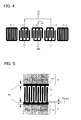
- FIG. 4 shows an exemplary configuration of the three-IDT multimode filters.
- reflective electrodes 5-1, 5-2 are provided adjacent to IDT 1-1 and IDT 1-3, so as to increase the energy concentration.
- a surface acoustic wave resonator having a filter characteristic using a resonance characteristic is structured.
- a transition region as a frequency difference between a point on the low frequency side of the passband (-4 dB point) and a so-called skirt portion of the filter of -50 DB, variations of the transition region against the sizes of the tip gap are compared.
- This transition region signifies that the filter becomes close to an ideal rectangular characteristic when the transition region approaches '0 MHz'.
- the transition region is approximately 12 MHz when tip gaps 4, 4' have a value 0.25 ⁇ which is generally applied to the conventional filter.
- the narrower the tip gap is set the more the mode profile is concentrated to the central part of the electrode finger, and the transition region is improved.
- the tip gap size is to be set no greater than 0.2 ⁇ .
- a tip gap size of at least 0.1 ⁇ m is necessary in view of a limit in manufacturing capability. This figure is dependent on the etching technique in the semiconductor process.
- FIG. 3 shows a diagram illustrating a passing characteristic of a three-IDT multimode filter when tip gaps 4, 4' are varied. There is shown the passing characteristic against tip gaps 4, 4' of 0.15 ⁇ (II) and 0.50 ⁇ (III), which are referenced from 0.25 ⁇ (I). It is to be understood, from the characteristic shown in FIG. 3, that the smaller the tip gaps 4, 4' are set, the more the insertion loss is improved (reduced) particularly on the low frequency side, in a corresponding manner to the variation of the transition region shown in FIG. 2.
- FIG. 5 shows an enlarged diagram of only one IDT in the three-IDT multimode filter structure shown in FIG. 4. Electrode fingers 2, 2' are connected to bus bars 3, 3' respectively, disposed on opposite sides (ends) of electrode fingers 2, 2'. Further, according to the embodiment the part of which is shown in FIG. 5, there are formed thick film electrodes on bus bars 3, 3', each accumulated on an area 31 (31') and positioned with (at) a distance M away from the connection face of electrode finger 2 (2') to bus bar 3 (3'). In the following description of the present embodiment, this distance M is defined as a thick film margin.
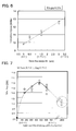
- FIG. 6 shows a diagram illustrating a measured result of a relationship between the thick film margin M and a transition region.
- the filter used in this measurement has the structure of the three-IDT multimode filter explained earlier. It is understood from FIG. 6 that the more the thick film margin M approaches '0', the more the transition region is improved. As already illustrated in FIG. 2, a good filter characteristic is acquired when the transition region is not greater than 11 MHz for the center frequency of approximately 1.9 MHz. From FIG. 6, the thick film margin M satisfying this condition is no greater than 0.75 ⁇ . As for the lower limit, if M is not greater than 0 ⁇ , electrode fingers 2, 2' may undesirably be short-circuited with bus bars 3, 3'. Therefore, there is a certain limit derived from the limit in manufacturing.
- the inventors of the present invention have examined the thickness of thick film additionally accumulated on the thick film areas of bus bars 3, 3'.
- FIG. 7 shows a diagram illustrating a relationship between an additional film thickness accumulated on bus bars 3, 3' and a minimum filter insertion loss.
- the additional film thickness denotes a film thickness added to the electrode thickness by further accumulating film on the areas of the thick film margin M of electrode fingers 2, 2' and bus bars 3, 3' in IDT 1.
- the filter used here has the same structure as the three-IDTmultimode filter described earlier.
- the chart shown in FIG. 7 depicts measured values, which are obtained under the condition that the thick film margin M is 0.5 ⁇ , and each of the gaps 4, 4' between electrode fingers 2, 2' and bus bars 3, 3' is 0. 25 ⁇ .
- the additional film thickness is to be set no smaller than 0.05 ⁇ . Further, if the additional film thickness is set no smaller than 0.05 ⁇ and no greater than 0.35 ⁇ , a preferable filter characteristic having an insertion loss of no greater than -2 dB may be obtained.
- thick film is used for the thick film to be accumulated on bus bars 3, 3'.
- Au gold
- thick films 31, 31' accumulated on bus bars 3, 3' may be an insulating material such as SiO 2 , because the purpose is to reduce the acoustic wave velocity. By using such an insulating material, it becomes possible to avoid short circuits between electrode fingers 2, 2' and bus bars 3, 3' in IDT 1.
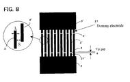
- FIG. 8 shows an exemplary embodiment of a filter structure where dummy electrodes are provided in the IDT. Dummy electrodes 21, 21' are attached at the tip gaps 4, 4' between electrode fingers 2, 2' and bus bars 3, 3' of the IDT.
- FIG. 8 an enlarged diagram of the portion enclosed by a circle is shown on the top left, in which an electrode width L of each electrode finger 2, 2' and a neighboring distance S between electrode fingers 2, 2' are shown.
- FIG. 9 and FIG. 10 illustrate characteristic diagrams of a three-IDT multimode filter for 900 MHz band.
- this multimode filter 42-degree Y-cut LiTaO 3 is employed as substrate material, and the ratio L/S of the electrode width L to the space S between the neighboring electrode fingers is set to approximately 0.7.
- FIG. 9 illustrates characteristic differences between cases of providing and not providing dummy electrodes. It is understood from the figure that there is an improved (reduced) loss on the low frequency side of the passband in the two samples having dummy electrodes 21, 21' of 1 ⁇ - 31 ⁇ (A1 and A2, in FIG. 9), as compared to the sample having no dummy electrodes 21, 21' (B in FIG. 9).
- FIG. 10 a characteristic for the case of varied tip gaps 4, 4' is shown in FIG. 10. It is understood that the loss is further improved on the low frequency side of the passband in the two samples (B1, B2 in FIG. 10: 0.09 ⁇ ), when the tip gaps are set narrower than in the ordinary case (A in FIG. 10) having gaps of 0.25 ⁇ .
- the L/S of the multimode filter is set to approximately 0.7.
- a wideband low-loss filter characteristic is obtainable when the L/S is set roughly in the range of 0.6 - 0.8, which has been confirmed by the inventors of the present invention.
- the present invention enables efficient transverse energy confinement, and provision of a surface acoustic wave filter having preferable characteristics of both insertion loss and shape factor.
Landscapes
- Physics & Mathematics (AREA)
- Acoustics & Sound (AREA)
- Surface Acoustic Wave Elements And Circuit Networks Thereof (AREA)
Abstract
Description
that this concentrated energy results in an insertion loss generated in the filter.
Claims (16)
- A surface acoustic wave device comprising:wherein, the electrode fingers of one comb electrode are disposed alternately between the electrode fingers of the other comb electrode, anda pair of reflective electrodes formed on a single-crystal piezoelectric substrate; andat least one set of comb electrodes formed between the pair of reflective electrodes,each comb electrode constituting the comb electrode set including:a plurality of electrode fingers; anda bus bar connecting the plurality of electrode fingers in common;
a thick film thicker than each plurality of electrode fingers is produced in a partial area of each bus bar, and
a tip gap is provided between the top of each electrode finger of one comb electrode and the end face of the opposed bus bar of the other comb electrode, with a distance therebetween set not greater than 0.2λ (where λ is one period of the comb electrode). - A surface acoustic wave device comprising:wherein, the electrode fingers of one comb electrode are disposed alternately between the electrode fingers of the other comb electrode, anda pair of reflective electrodes formed on a single-crystal piezoelectric substrate; andat least one set of comb electrodes formed between the pair of reflective electrodes,each comb electrode constituting the comb electrode set including:a plurality of electrode fingers and a plurality of dummy electrodes disposed alternately; anda bus bar connecting the plurality of electrode fingers and the plurality of dummy electrodes in common;
a tip gap is provided between the top of each electrode finger of one comb electrode and the top of the opposed dummy electrode of the other comb electrode, with a distance therebetween set not greater than 0.2λ (where λ is one period of the comb electrode). - A surface acoustic wave device comprising:wherein, the electrode fingers of one comb electrode are disposed alternately between the electrode fingers of the other comb electrode, anda pair of reflective electrodes formed on a single-crystal piezoelectric substrate; andthree sets of comb electrodes formed between the pair of reflective electrodes,each comb electrode constituting the comb electrode set including:a plurality of electrode fingers and a plurality of dummy electrodes disposed alternately; anda bus bar connecting the plurality of electrode fingers and the plurality of dummy electrodes in common;
a tip gap is provided between the top of each electrode finger of one comb electrode and the top of the opposed dummy electrode of the other comb electrode, with a distance therebetween set not greater than 0.2λ (where, λ is one period of the comb electrode). - A surface acoustic wave device comprising a plurality of resonators connected into a ladder shape, each resonator including:wherein, the electrode fingers of one comb electrode are disposed alternately between the electrode fingers of the other comb electrode, anda pair of reflective electrodes formed on a single-crystal piezoelectric substrate; andat least one set of comb electrodes formed between the pair of reflective electrodes,each comb electrode of the comb electrode set constituting the resonator having:a plurality of electrode fingers and a plurality of dummy electrodes disposed alternately; anda bus bar connecting the plurality of electrode fingers and the plurality of dummy electrodes in common;
a tip gap is provided between the top of each electrode finger of one comb electrode and the top of the opposed dummy electrode of the other comb electrode, with a distance therebetween set not greater than 0.2λ (where λ is one period of the comb electrode). - A surface acoustic wave device comprising a plurality of resonators connected into a lattice shape, each resonator including:wherein, the electrode fingers of one comb electrode are disposed alternately between the electrode fingers of the other comb electrode, anda pair of reflective electrodes formed on a single-crystal piezoelectric substrate; andat least one set of comb electrodes formed between the pair of reflective electrodes,each comb electrode of the comb electrode set constituting the resonator having:a plurality of electrode fingers and a plurality of dummy electrodes disposed alternately; anda bus bar connecting the plurality of electrode fingers and the plurality of dummy electrodes in common;
a tip gap is provided between the top of each electrode finger of one comb electrode and the top of the opposed dummy electrode of the other comb electrode, with a distance therebetween set not greater than 0.2λ (where λ is one period of the comb electrode). - A surface acoustic wave device comprising:wherein, the electrode fingers of one comb electrode are disposed alternately between the electrode fingers of the other comb electrode, anda pair of reflective electrodes formed on a single-crystal piezoelectric substrate; andthree sets of comb electrodes formed between the pair of reflective electrodes,each comb electrode forming the comb electrode set including:a plurality of electrode fingers; anda bus bar connecting the plurality of electrode fingers in common;
thick film thicker than each plurality of electrode fingers is produced in partial areas of each bus bar, and
a tip gap is provided between the top of each electrode finger of one comb electrode and the end face of the opposed bus bar of the other comb electrode, with a distance therebetween set not greater than 0.2λ (where, λ is one period of the comb electrode). - A surface acoustic wave device comprising a plurality of resonators connected into a ladder shape, each resonator including:wherein, the electrode fingers of one comb electrode are disposed alternately between the electrode fingers of the other comb electrode, anda pair of reflective electrodes formed on a single-crystal piezoelectric substrate; andat least one set of comb electrodes formed between the pair of reflective electrodes,each comb electrode of the comb electrode set constituting the resonator having:a plurality of electrode fingers; anda bus bar connecting the plurality of electrode fingers in common;
thick film thicker than each plurality of electrode fingers is produced in partial areas of each bus bar, and
a tip gap is provided between the top of each electrode finger of one comb electrode and the end face of the opposed bus bar of the other comb electrode, with a distance therebetween set not greater than 0.2λ (where λ is one period of the comb electrode). - A surface acoustic wave device comprising a plurality of resonators connected into a lattice shape, each resonator including:wherein, the electrode fingers of one comb electrode are disposed alternately between the electrode fingers of the other comb electrode, anda pair of reflective electrodes formed on a single-crystal piezoelectric substrate; andat least one set of comb electrodes formed between the pair of reflective electrodes,each comb electrode of the comb electrode set constituting the resonator having:a plurality of electrode fingers; anda bus bar connecting the plurality of electrode fingers in common;
thick film thicker than each plurality of electrode fingers is produced in partial areas of each bus bar, and
a tip gap is provided between the top of each electrode finger of one comb electrode and the end face of the opposed bus bar of the other comb electrode, with a distance therebetween set not greater than 0.2λ (where λ is one period of the comb electrode). - The surface acoustic wave device according to any of claims 2 to 5,
wherein, thick film thicker than each plurality of electrode fingers is further produced in partial areas of each bus bar. - The surface acoustic wave device according to claim 3 or claim 6,
wherein, a ratio L/S of an electrode width L of an electrode finger to a space S between neighboring electrode fingers is set to between 0.6 and 0.8. - The surface acoustic wave device according to any one of claim 1 and claims 6 to 8,
wherein, for each comb electrode, each partial area of the bus bar on which the thick film is produced is disposed at a distance of not greater than 0.75λ from the connection end face of the bus bar connecting to the plurality of electrode fingers (where λ is one period of the comb electrode). - The surface acoustic wave device according to any one of claim 1 and claims 6 to 8,
wherein, for each comb electrode, the plurality of electrode fingers and the bus bar connecting the plurality of electrode fingers are formed of metal of which the principal component is aluminium, and each partial area of the bus bar in which the thick film is produced has an additional thickness of at least 0.05λ more than the film thickness of the plurality of electrode fingers (where λ is one period of the comb electrode). - The surface acoustic wave device according to claim 12,
wherein, preferably, each partial area of the bus bar in which the thick film is produced has an additional thickness of not greater than 0.35λ more than the film thickness of the plurality of electrode fingers (where λ is one period of the comb electrode). - The surface acoustic wave device according to any one of claim 1 and claims 6 to 8,
wherein, for each comb electrode, the thick film in each said partial area of the bus bar is formed of heavy metal. - The surface acoustic wave device according to any one of claim 1 and claims 6 to 8,
wherein, for each comb electrode, the thick film in each said partial area of the bus bar is formed of insulating material. - The surface acoustic wave device according to any preceding claim,
wherein a single-crystal piezoelectric substrate is formed of LiTaO3 or LiNbO3, and the device is for use with a leaky surface acoustic wave of the substrate.
Applications Claiming Priority (2)
| Application Number | Priority Date | Filing Date | Title |
|---|---|---|---|
| JP2003118090 | 2003-04-23 | ||
| JP2003118090A JP3929415B2 (en) | 2003-04-23 | 2003-04-23 | Surface acoustic wave device |
Publications (2)
| Publication Number | Publication Date |
|---|---|
| EP1471638A2 true EP1471638A2 (en) | 2004-10-27 |
| EP1471638A3 EP1471638A3 (en) | 2005-09-07 |
Family
ID=32959624
Family Applications (1)
| Application Number | Title | Priority Date | Filing Date |
|---|---|---|---|
| EP04252353A Withdrawn EP1471638A3 (en) | 2003-04-23 | 2004-04-21 | Surface acoustic wave device |
Country Status (5)
| Country | Link |
|---|---|
| US (1) | US7170371B2 (en) |
| EP (1) | EP1471638A3 (en) |
| JP (1) | JP3929415B2 (en) |
| KR (1) | KR100729694B1 (en) |
| CN (1) | CN100474765C (en) |
Cited By (1)
| Publication number | Priority date | Publication date | Assignee | Title |
|---|---|---|---|---|
| WO2007073722A1 (en) * | 2005-12-23 | 2007-07-05 | Epcos Ag | Acoustic wave transducer and filter comprising said transducer |
Families Citing this family (13)
| Publication number | Priority date | Publication date | Assignee | Title |
|---|---|---|---|---|
| JP2006319887A (en) * | 2005-05-16 | 2006-11-24 | Murata Mfg Co Ltd | Elastic boundary wave device |
| JP4465625B2 (en) * | 2006-09-29 | 2010-05-19 | Tdk株式会社 | Surface acoustic wave filter and surface acoustic wave resonator |
| KR100884374B1 (en) | 2008-05-08 | 2009-02-17 | 주식회사 씨-테크 | Heterogeneous intercommunication module for communication |
| US9136458B2 (en) | 2011-03-22 | 2015-09-15 | Skyworks Panasonic Filter Solutions Japan Co., Ltd. | Elastic wave element |
| US9337800B1 (en) * | 2011-10-12 | 2016-05-10 | Sandia Corporation | Microresonator electrode design |
| JP5989524B2 (en) * | 2012-11-30 | 2016-09-07 | 京セラ株式会社 | Elastic wave device, duplexer and communication module |
| JP6335473B2 (en) | 2013-11-01 | 2018-05-30 | 太陽誘電株式会社 | Surface acoustic wave device and filter |
| JP6355328B2 (en) | 2013-12-19 | 2018-07-11 | 太陽誘電株式会社 | Surface acoustic wave device and filter |
| JP6284800B2 (en) | 2014-03-26 | 2018-02-28 | 太陽誘電株式会社 | Surface acoustic wave device and filter |
| US10951194B2 (en) * | 2017-12-20 | 2021-03-16 | Kyocera Corporation | Acoustic wave filter, multiplexer, and communication apparatus |
| JP7203578B2 (en) * | 2018-11-14 | 2023-01-13 | NDK SAW devices株式会社 | surface acoustic wave element |
| JP7178881B2 (en) * | 2018-11-16 | 2022-11-28 | NDK SAW devices株式会社 | surface acoustic wave element |
| JP2022012383A (en) * | 2020-07-01 | 2022-01-17 | 株式会社村田製作所 | Filter device, multiplexer, and communication device |
Family Cites Families (24)
| Publication number | Priority date | Publication date | Assignee | Title |
|---|---|---|---|---|
| JPS5657526U (en) * | 1979-10-11 | 1981-05-18 | ||
| JPH05235684A (en) * | 1992-02-25 | 1993-09-10 | Tdk Corp | Multielectrode type surface acoustic wave device |
| JPH06232682A (en) * | 1993-02-08 | 1994-08-19 | Hitachi Ltd | Surface acoustic wave resonator and surface acoustic wave filter |
| US5710529A (en) * | 1993-10-15 | 1998-01-20 | Ngk Insulators, Ltd. | Surface acoustic wave filer device having a cascade filter structure and a piezoelectric substrate having mirror-polished surfaces |
| JPH08139557A (en) * | 1994-09-14 | 1996-05-31 | Ngk Insulators Ltd | Surface acoustic wave filter device |
| GB2296614B (en) * | 1994-12-23 | 1999-09-15 | Advanced Saw Prod Sa | Saw filter |
| JPH0946163A (en) * | 1995-07-31 | 1997-02-14 | Kinseki Ltd | Surface acoustic wave filter |
| JP3226472B2 (en) * | 1996-05-14 | 2001-11-05 | 富士通株式会社 | Surface acoustic wave multimode filter |
| JPH1117493A (en) | 1997-06-19 | 1999-01-22 | Tdk Corp | Surface acoustic wave device |
| WO1999005788A1 (en) * | 1997-07-28 | 1999-02-04 | Kabushiki Kaisha Toshiba | Surface acoustic wave device and method of producing the same |
| JPH1174753A (en) * | 1997-08-29 | 1999-03-16 | Kinseki Ltd | Surface acoustic wave filter |
| JPH11191720A (en) * | 1997-12-25 | 1999-07-13 | Kyocera Corp | Surface acoustic wave device and surface acoustic wave filter |
| JPH11340774A (en) * | 1998-05-26 | 1999-12-10 | Murata Mfg Co Ltd | Surface acoustic wave filter |
| JP3587354B2 (en) | 1999-03-08 | 2004-11-10 | 株式会社村田製作所 | Laterally coupled resonator type surface acoustic wave filter and longitudinally coupled resonator type surface acoustic wave filter |
| JP3412611B2 (en) * | 2000-09-25 | 2003-06-03 | 株式会社村田製作所 | Surface acoustic wave device |
| JP2002176333A (en) * | 2000-12-07 | 2002-06-21 | Fujitsu Media Device Kk | Surface acoustic wave filter |
| US6714102B2 (en) * | 2001-03-01 | 2004-03-30 | Agilent Technologies, Inc. | Method of fabricating thin film bulk acoustic resonator (FBAR) and FBAR structure embodying the method |
| JP3498215B2 (en) * | 2001-04-09 | 2004-02-16 | 株式会社村田製作所 | Surface acoustic wave filter, surface acoustic wave device, and communication device |
| JP2003087080A (en) * | 2001-07-06 | 2003-03-20 | Murata Mfg Co Ltd | Surface acoustic wave device and method of manufacturing the same |
| JP3963253B2 (en) * | 2001-12-14 | 2007-08-22 | 富士通メディアデバイス株式会社 | Surface acoustic wave device and duplexer using the same |
| JP2003198317A (en) * | 2001-12-21 | 2003-07-11 | Fujitsu Media Device Kk | Surface acoustic wave resonator and surface acoustic wave filter |
| JP3846409B2 (en) * | 2002-02-15 | 2006-11-15 | 株式会社村田製作所 | Surface acoustic wave device, communication device |
| JP2004343259A (en) * | 2003-05-13 | 2004-12-02 | Matsushita Electric Ind Co Ltd | Surface acoustic wave filter |
| JP4100249B2 (en) * | 2003-05-19 | 2008-06-11 | 株式会社村田製作所 | Surface acoustic wave device, communication device |
-
2003
- 2003-04-23 JP JP2003118090A patent/JP3929415B2/en not_active Expired - Lifetime
-
2004
- 2004-04-14 US US10/823,648 patent/US7170371B2/en not_active Expired - Lifetime
- 2004-04-21 EP EP04252353A patent/EP1471638A3/en not_active Withdrawn
- 2004-04-22 KR KR1020040027725A patent/KR100729694B1/en not_active Expired - Lifetime
- 2004-04-23 CN CNB2004100375117A patent/CN100474765C/en not_active Expired - Lifetime
Cited By (2)
| Publication number | Priority date | Publication date | Assignee | Title |
|---|---|---|---|---|
| WO2007073722A1 (en) * | 2005-12-23 | 2007-07-05 | Epcos Ag | Acoustic wave transducer and filter comprising said transducer |
| US7868717B2 (en) | 2005-12-23 | 2011-01-11 | Epcos Ag | Acoustic wave transducer and filter comprising said transducer |
Also Published As
| Publication number | Publication date |
|---|---|
| JP2004328196A (en) | 2004-11-18 |
| CN1540860A (en) | 2004-10-27 |
| EP1471638A3 (en) | 2005-09-07 |
| CN100474765C (en) | 2009-04-01 |
| US7170371B2 (en) | 2007-01-30 |
| US20040251990A1 (en) | 2004-12-16 |
| KR20040092454A (en) | 2004-11-03 |
| JP3929415B2 (en) | 2007-06-13 |
| KR100729694B1 (en) | 2007-06-18 |
Similar Documents
| Publication | Publication Date | Title |
|---|---|---|
| US6570470B2 (en) | Surface acoustic wave ladder filter utilizing parallel resonators with different resonant frequencies | |
| CN100365929C (en) | Surface Acoustic Wave Resonators and Surface Filters | |
| US10171061B2 (en) | Elastic wave device | |
| US7939989B2 (en) | Piston mode acoustic wave device and method providing a high coupling factor | |
| US9035725B2 (en) | Acoustic wave device | |
| CN106664074B (en) | Elastic wave element, filter element, and communication device | |
| CN1325562A (en) | Surface wave device with at least two surface wave structures | |
| EP2128982A1 (en) | Elastic wave device | |
| EP1471638A2 (en) | Surface acoustic wave device | |
| US8803402B2 (en) | Elastic wave device | |
| EP2202882A1 (en) | Surface acoustic wave resonator and ladder type filter | |
| US7439827B2 (en) | Surface acoustic wave filter device | |
| JPH07307640A (en) | Surface acoustic wave device | |
| US20250062742A1 (en) | Electroacoustic resonator | |
| US7453334B1 (en) | Leaky SAW resonator and method | |
| KR19980069740A (en) | Surface acoustic wave multi-mode filter | |
| WO2003050949A1 (en) | Surface acoustic wave filter | |
| US20060220494A1 (en) | Elastic boundary wave device, resonator, and ladder-type filter | |
| US20060131992A1 (en) | One-port surface acoustic wave resonator and surface acoustic wave filter | |
| US6828879B2 (en) | Longitudinal coupled multiple mode surface acoustic wave filter | |
| JP3890740B2 (en) | Surface acoustic wave waveguide structure and device using the same | |
| JP3107392B2 (en) | Vertically coupled dual mode leaky SAW filter | |
| WO2024225181A1 (en) | Elastic wave resonator and communication device | |
| CN118337172A (en) | Surface acoustic wave filter | |
| JP2000224003A (en) | Vertically coupled dual mode SAW filter |
Legal Events
| Date | Code | Title | Description |
|---|---|---|---|
| PUAI | Public reference made under article 153(3) epc to a published international application that has entered the european phase |
Free format text: ORIGINAL CODE: 0009012 |
|
| AK | Designated contracting states |
Kind code of ref document: A2 Designated state(s): AT BE BG CH CY CZ DE DK EE ES FI FR GB GR HU IE IT LI LU MC NL PL PT RO SE SI SK TR |
|
| AX | Request for extension of the european patent |
Extension state: AL HR LT LV MK |
|
| PUAL | Search report despatched |
Free format text: ORIGINAL CODE: 0009013 |
|
| AK | Designated contracting states |
Kind code of ref document: A3 Designated state(s): AT BE BG CH CY CZ DE DK EE ES FI FR GB GR HU IE IT LI LU MC NL PL PT RO SE SI SK TR |
|
| AX | Request for extension of the european patent |
Extension state: AL HR LT LV MK |
|
| 17P | Request for examination filed |
Effective date: 20060301 |
|
| AKX | Designation fees paid |
Designated state(s): DE FR GB |
|
| 17Q | First examination report despatched |
Effective date: 20070119 |
|
| STAA | Information on the status of an ep patent application or granted ep patent |
Free format text: STATUS: THE APPLICATION IS DEEMED TO BE WITHDRAWN |
|
| 18D | Application deemed to be withdrawn |
Effective date: 20090818 |