JP7178881B2 - surface acoustic wave element - Google Patents
surface acoustic wave element Download PDFInfo
- Publication number
- JP7178881B2 JP7178881B2 JP2018215986A JP2018215986A JP7178881B2 JP 7178881 B2 JP7178881 B2 JP 7178881B2 JP 2018215986 A JP2018215986 A JP 2018215986A JP 2018215986 A JP2018215986 A JP 2018215986A JP 7178881 B2 JP7178881 B2 JP 7178881B2
- Authority
- JP
- Japan
- Prior art keywords
- region
- surface acoustic
- acoustic wave
- propagation speed
- busbar
- Prior art date
- Legal status (The legal status is an assumption and is not a legal conclusion. Google has not performed a legal analysis and makes no representation as to the accuracy of the status listed.)
- Active
Links
Images


Classifications
-
- H—ELECTRICITY
- H03—ELECTRONIC CIRCUITRY
- H03H—IMPEDANCE NETWORKS, e.g. RESONANT CIRCUITS; RESONATORS
- H03H9/00—Networks comprising electromechanical or electro-acoustic devices; Electromechanical resonators
- H03H9/02—Details
- H03H9/125—Driving means, e.g. electrodes, coils
- H03H9/145—Driving means, e.g. electrodes, coils for networks using surface acoustic waves
- H03H9/14538—Formation
- H03H9/14541—Multilayer finger or busbar electrode
-
- H—ELECTRICITY
- H03—ELECTRONIC CIRCUITRY
- H03H—IMPEDANCE NETWORKS, e.g. RESONANT CIRCUITS; RESONATORS
- H03H9/00—Networks comprising electromechanical or electro-acoustic devices; Electromechanical resonators
- H03H9/02—Details
- H03H9/02535—Details of surface acoustic wave devices
- H03H9/02818—Means for compensation or elimination of undesirable effects
- H03H9/02834—Means for compensation or elimination of undesirable effects of temperature influence
-
- H—ELECTRICITY
- H03—ELECTRONIC CIRCUITRY
- H03H—IMPEDANCE NETWORKS, e.g. RESONANT CIRCUITS; RESONATORS
- H03H9/00—Networks comprising electromechanical or electro-acoustic devices; Electromechanical resonators
- H03H9/02—Details
- H03H9/02535—Details of surface acoustic wave devices
-
- H—ELECTRICITY
- H03—ELECTRONIC CIRCUITRY
- H03H—IMPEDANCE NETWORKS, e.g. RESONANT CIRCUITS; RESONATORS
- H03H3/00—Apparatus or processes specially adapted for the manufacture of impedance networks, resonating circuits, resonators
- H03H3/007—Apparatus or processes specially adapted for the manufacture of impedance networks, resonating circuits, resonators for the manufacture of electromechanical resonators or networks
- H03H3/08—Apparatus or processes specially adapted for the manufacture of impedance networks, resonating circuits, resonators for the manufacture of electromechanical resonators or networks for the manufacture of resonators or networks using surface acoustic waves
-
- H—ELECTRICITY
- H03—ELECTRONIC CIRCUITRY
- H03H—IMPEDANCE NETWORKS, e.g. RESONANT CIRCUITS; RESONATORS
- H03H9/00—Networks comprising electromechanical or electro-acoustic devices; Electromechanical resonators
- H03H9/02—Details
- H03H9/125—Driving means, e.g. electrodes, coils
- H03H9/145—Driving means, e.g. electrodes, coils for networks using surface acoustic waves
- H03H9/14517—Means for weighting
- H03H9/1452—Means for weighting by finger overlap length, apodisation
-
- H—ELECTRICITY
- H03—ELECTRONIC CIRCUITRY
- H03H—IMPEDANCE NETWORKS, e.g. RESONANT CIRCUITS; RESONATORS
- H03H9/00—Networks comprising electromechanical or electro-acoustic devices; Electromechanical resonators
- H03H9/02—Details
- H03H9/125—Driving means, e.g. electrodes, coils
- H03H9/145—Driving means, e.g. electrodes, coils for networks using surface acoustic waves
- H03H9/14517—Means for weighting
- H03H9/14529—Distributed tap
- H03H9/14532—Series weighting; Transverse weighting
-
- H—ELECTRICITY
- H03—ELECTRONIC CIRCUITRY
- H03H—IMPEDANCE NETWORKS, e.g. RESONANT CIRCUITS; RESONATORS
- H03H9/00—Networks comprising electromechanical or electro-acoustic devices; Electromechanical resonators
- H03H9/02—Details
- H03H9/125—Driving means, e.g. electrodes, coils
- H03H9/145—Driving means, e.g. electrodes, coils for networks using surface acoustic waves
- H03H9/14544—Transducers of particular shape or position
- H03H9/14552—Transducers of particular shape or position comprising split fingers
-
- H—ELECTRICITY
- H03—ELECTRONIC CIRCUITRY
- H03H—IMPEDANCE NETWORKS, e.g. RESONANT CIRCUITS; RESONATORS
- H03H9/00—Networks comprising electromechanical or electro-acoustic devices; Electromechanical resonators
- H03H9/02—Details
- H03H9/125—Driving means, e.g. electrodes, coils
- H03H9/145—Driving means, e.g. electrodes, coils for networks using surface acoustic waves
- H03H9/14544—Transducers of particular shape or position
- H03H9/1457—Transducers having different finger widths
-
- H—ELECTRICITY
- H03—ELECTRONIC CIRCUITRY
- H03H—IMPEDANCE NETWORKS, e.g. RESONANT CIRCUITS; RESONATORS
- H03H9/00—Networks comprising electromechanical or electro-acoustic devices; Electromechanical resonators
- H03H9/25—Constructional features of resonators using surface acoustic waves
Description
本発明は周波数信号を弾性表面波に変換する弾性表面波素子に関する。 The present invention relates to a surface acoustic wave device for converting frequency signals into surface acoustic waves.
Q値が高くスプリアスの少ない弾性表面波素子として、ピストンモードで動作するものが開発されている(例えば特許文献1、2)。ピストンモードは、弾性表面波(SAW:Surface Acoustic Wave)の振動モードの1つであり、後述の図1(c)に示すように、励振領域ではSAWの振幅がほぼ一定である一方、その外部側の領域にて急激に振幅が減少する振幅分布を示す。
As a surface acoustic wave device with a high Q value and little spurious, a device that operates in a piston mode has been developed (for example,
SAWの励振にあたっては、バスバーに多数の電極指を接続した櫛歯電極が用いられる。弾性表面波素子(SAW素子)は、電極指の並び方向に見て、電極指が交差するように2つの櫛歯電極を対向して配置したIDT(Interdigital Transducer)電極が設けられる。一方の櫛歯電極に所定の周波数を有する周波数信号を入力することによりSAWが励振され、他方の櫛歯電極へと伝播する。 For SAW excitation, a comb-tooth electrode having a large number of electrode fingers connected to a bus bar is used. A surface acoustic wave element (SAW element) is provided with an IDT (Interdigital Transducer) electrode in which two comb-teeth electrodes are arranged to face each other so that the electrode fingers intersect when viewed in the direction in which the electrode fingers are arranged. By inputting a frequency signal having a predetermined frequency to one of the comb electrodes, the SAW is excited and propagates to the other comb electrodes.
特許文献1、2に記載の技術は、対向して配置された2つのバスバー間の領域について、バスバーが伸びる方向に沿って中央の領域、その両脇の2領域、さらに両脇の2領域の5つ(特許文献1:中央領域、エッジ領域、ギャップ領域、特許文献2:中央励起領域、内縁領域、外縁領域)に分けている。そして、中央の両脇の領域に位置する電極指(特許文献1は「電極部」と記載)の幅を大きくしたり、狭くしたりすることなどによりピストンモードを得ている。また、特許文献1では、ギャップ領域のギャップ長寸法を1~3音響波長程度確保する必要がある旨が記載されている。
In the techniques described in
しかしながらこれらの手法は、通常のIDT電極に比べギャップ長の寸法(特許文献1のギャップ領域や特許文献2の外縁領域の寸法)が長くなるため、素子(特許文献1:音響波装置、特許文献2:電気音響変換器)が大型化してしまう問題がある。
However, in these methods, the dimension of the gap length (the dimension of the gap region of
本発明はこのような事情の下になされたものであり、ピストンモードの励振が可能な小型の弾性表面波素子を提供する。 The present invention has been made under such circumstances, and provides a small-sized surface acoustic wave device capable of excitation in a piston mode.
本弾性表面波素子は、圧電基板と、
前記圧電基板上に形成された一対のバスバーと、これらバスバーの各々から対向するバスバーに向かって互いに櫛歯状に伸び出す複数の電極指と、を備え、これら複数の電極指の並び方向に沿って見たとき、一方のバスバーに接続された電極指と、他方のバスバーに接続された電極指とが交差する領域である交差領域が形成された一対のIDT電極と、を備え、
前記交差領域の端部側の領域であって、前記複数の電極指の先端部を含み、前記バスバーに沿って伸びる帯状の領域をエッジ領域と呼ぶとき、前記エッジ領域での弾性表面波の伝播速度が、前記交差領域での弾性表面波の伝播速度より低速であることと、
前記交差領域における弾性表面波の伝播速度よりも、前記バスバーが設けられた領域であるバスバー領域における弾性表面波の伝播速度が高速であることと、
前記一対のバスバーの各々について、一方のバスバーに接続された複数の電極指の先端部と、他方のバスバーとの間に、これらの先端部から離れて、他方のバスバーから伸び出す複数のダミー電極が形成され、前記ダミー電極を含み、前記バスバーに沿って伸びる帯状の領域であるダミー電極領域における弾性表面波の伝播速度が、前記エッジ領域での弾性表面波の伝播速度よりも高速、且つ、前記バスバー領域での弾性表面波の伝播速度よりも低速であり、さらに、前記エッジ領域と前記ダミー電極領域とに挟まれたギャップ領域では、弾性表面波の伝播速度が、前記バスバー領域での弾性表面波の伝播速度よりも高速であることを特徴とする。また、前記ダミー電極が形成され、前記バスバーに沿って伸びる帯状の領域をダミー領域と呼ぶとき、前記ダミー電極及び前記IDT電極の前記ダミー領域内に位置する部分には、前記弾性表面波の伝播速度を低下させるための伝播速度調節膜が形成されていてもよい。
The surface acoustic wave device includes a piezoelectric substrate,
a pair of busbars formed on the piezoelectric substrate; and a plurality of electrode fingers extending from each of the busbars toward the opposing busbars in a comb-teeth shape; When viewed from above, a pair of IDT electrodes in which an intersection region is formed where an electrode finger connected to one bus bar and an electrode finger connected to the other bus bar intersect,
When a band-like region extending along the bus bar, which is a region on the end side of the intersection region and includes the tips of the plurality of electrode fingers, is called an edge region, surface acoustic waves propagate in the edge region. the velocity is lower than the propagation velocity of surface acoustic waves in the intersection region;
The propagation speed of the surface acoustic waves in the busbar region, which is the region where the busbars are provided, is higher than the propagation speed of the surface acoustic waves in the intersection region;
For each of the pair of busbars, a plurality of dummy electrodes extending from the other busbar away from the tips of the plurality of electrode fingers connected to one busbar and the other busbar. is formed, and the surface acoustic wave propagation speed in the dummy electrode region, which is a strip-shaped region that includes the dummy electrode and extends along the bus bar, is higher than the propagation speed of the surface acoustic wave in the edge region, and The propagation speed of the surface acoustic wave is lower than that in the busbar region, and furthermore, in the gap region sandwiched between the edge region and the dummy electrode region, the propagation speed of the surface acoustic wave is lower than that of the elastic surface wave in the busbar region. It is characterized by being faster than the propagation speed of the surface wave. Further, when the band-shaped region in which the dummy electrode is formed and extends along the bus bar is called a dummy region, a portion of the dummy electrode and the IDT electrode located in the dummy region has a surface acoustic wave propagating region. A propagation speed control film may be formed to reduce the speed.
上述の弾性表面波素子は、以下の構成を備えていてもよい。
(a)前記IDT電極の前記エッジ領域内に位置する部分には、前記交差領域よりも弾性表面波の伝播速度を低下させるための伝播速度調節膜が形成されていること。または、前記エッジ領域内に位置する電極指には、前記交差領域よりも弾性表面波の伝播速度を低下させるための拡幅部が形成されていること。
(b)前記交差領域よりもバスバー領域における弾性表面波の伝播速度を高速にするため、前記電極指を構成する金属膜の厚さよりも、前記バスバーを構成する金属膜の厚さが薄いこと。
(c)前記交差領域よりもバスバー領域における弾性表面波の伝播速度を高速にするため、前記電極指を構成する金属膜の密度よりも、前記バスバーを構成する金属膜の密度が小さいこと。
(d)前記IDT電極よりも上層側には、前記圧電基板の温度-周波数特性とは反対の方向に周波数が変化する温度-周波数特性を有する誘電体膜が形成されていること。
(e)前記交差領域よりもバスバー領域における弾性表面波の伝播速度を高速にするため、電極指が配置された電極指領域に形成された誘電体膜の厚さよりも、前記バスバー領域に形成された誘電体膜の厚さが薄いこと。または、前記交差領域よりもバスバー領域における弾性表面波の伝播速度を高速にするため、電極指が配置された電極指領域には誘電体膜が形成され、前記バスバー領域には誘電体膜が形成されていないこと。
(f)前記交差領域よりもバスバー領域における弾性表面波の伝播速度を高速にするため、電極指が配置された電極指領域に形成された誘電体膜よりも、前記バスバー領域に形成された誘電体膜の方が、弾性表面波の伝播速度が速い誘電体により構成されていること。
(g)(d)~(f)において、前記圧電基板は、LiNbO3またはLiTaO3であり、前記誘電体膜は酸化ケイ素、酸窒化ケイ素またはフッ素ドープ酸化ケイ素であること。
The surface acoustic wave device described above may have the following configuration.
(a) A portion of the IDT electrode located within the edge region is formed with a propagation speed control film for lowering the propagation speed of the surface acoustic wave from that of the intersection region. Alternatively, the electrode fingers located in the edge region are formed with widened portions for lowering the propagation speed of surface acoustic waves than in the intersection region.
(b) The thickness of the metal film forming the busbar is thinner than the thickness of the metal film forming the electrode fingers in order to increase the propagation speed of the surface acoustic wave in the busbar region than in the intersection region.
(c) The density of the metal films forming the busbars is lower than the density of the metal films forming the electrode fingers in order to increase the propagation speed of surface acoustic waves in the busbar regions than in the crossing regions.
(d) A dielectric film having temperature-frequency characteristics in which the frequency changes in a direction opposite to the temperature-frequency characteristics of the piezoelectric substrate is formed above the IDT electrodes.
(e) In order to increase the propagation speed of the surface acoustic wave in the busbar region than in the intersection region, the thickness of the dielectric film formed in the electrode finger region where the electrode fingers are arranged is thicker than the thickness of the dielectric film formed in the busbar region. The thickness of the dielectric film should be thin. Alternatively, a dielectric film is formed in the electrode finger regions where the electrode fingers are arranged, and the dielectric film is formed in the busbar region in order to increase the propagation speed of the surface acoustic wave in the busbar region than in the intersection region. that it is not.
(f) a dielectric film formed in the busbar region rather than a dielectric film formed in the electrode finger region where the electrode fingers are arranged in order to increase the propagation speed of the surface acoustic wave in the busbar region than in the intersection region; The body film should be composed of a dielectric with a higher surface acoustic wave propagation velocity.
(g) In (d) to (f), the piezoelectric substrate is LiNbO 3 or LiTaO 3 and the dielectric film is silicon oxide, silicon oxynitride or fluorine-doped silicon oxide.
(h)隣り合って配置された電極指の中心線間の距離dに対し、当該電極指の延伸方向に沿って見た前記交差領域の端部とバスバーとの間幅が0.1d~2dの範囲内であること。
(i)弾性表面波素子に耐候性を持たせるため、あるいは周波数調整を行うために、当該弾性表面波素子の最上層に形成された上層膜を備えたこと。前記上層膜は窒化ケイ素であること。
(h ) With respect to the distance d between the center lines of the electrode fingers arranged adjacent to each other, the width between the end of the intersecting region and the busbar viewed along the extending direction of the electrode fingers is 0.1d to 0.1d. Must be within 2d.
( i ) An upper layer film is formed on the uppermost layer of the surface acoustic wave element in order to provide the surface acoustic wave element with weather resistance or to adjust the frequency. The upper layer film is silicon nitride.
本発明によれば、エッジ領域での弾性表面波の伝播速度を、交差領域での弾性表面波の伝播速度より低速とし、一対のIDT電極の電極指が交差する交差領域における弾性表面波の伝播速度よりも、バスバーが設けられたバスバー領域における弾性表面波の伝播速度を高速としているので、従来のIDT電極に長いギャップ長寸法を設けなくとも、ピストンモードの弾性表面波を励振することができる。 According to the present invention, the propagation speed of the surface acoustic wave in the edge region is made slower than the propagation speed of the surface acoustic wave in the intersection region, and the surface acoustic wave propagates in the intersection region where the electrode fingers of the pair of IDT electrodes intersect. Since the propagation speed of the surface acoustic wave in the busbar region where the busbar is provided is higher than the speed, it is possible to excite the piston-mode surface acoustic wave without providing a long gap length dimension in the conventional IDT electrode. .
はじめに、図1を参照しながら、本実施の形態に係る弾性表面波素子(SAW素子)にて、ピストンモードのSAWを励振させるための基本構成について説明する。
図1(a)はSAW素子を模式的に示した拡大平面図、図1(b)は、図1(a)中に示すY軸方向に沿って見たSAWの伝播速度の分布図、図1(c)は、同方向に沿って見たSAWの振幅の分布図である。
First, referring to FIG. 1, a basic configuration for exciting a piston-mode SAW in a surface acoustic wave device (SAW device) according to the present embodiment will be described.
FIG. 1(a) is an enlarged plan view schematically showing a SAW element, and FIG. 1(b) is a SAW propagation velocity distribution diagram viewed along the Y-axis direction shown in FIG. 1(a). 1(c) is a SAW amplitude distribution diagram viewed along the same direction.
本例のSAW素子は、SAWを励振させる矩形状の圧電基板11上に形成されたIDT電極を備える。以下の説明では、矩形状の圧電基板11の長辺に沿った方向を縦方向(図1(a)中のX方向)、短辺に沿った方向を横方向(同図中のY方向)ともいう。
The SAW element of this example includes IDT electrodes formed on a rectangular
IDT電極は、例えば圧電基板11の各長辺に沿って縦方向に伸びるように設けられ、各々信号ポート12a、12bに接続された2本のバスバー2a、2bと、各バスバー2a、2bから横方向に向けて伸びるように形成された多数本の電極指3a、3bとを備えている。
The IDT electrodes are provided, for example, so as to extend vertically along each long side of the
圧電基板11を構成する圧電材料としては、例えばニオブ酸リチウム(LiNbO3)やタンタル酸リチウム(LiTaO3)、窒化アルミニウム(AlN)、スカンジウム(Sc)ドープ窒化アルミニウムなどを用いる場合を例示することができる。
また、本実施の形態に係る圧電基板11には、(i)非圧電体材料からなる基板の表面に、圧電薄膜を形成したものや(ii)非圧電材料と圧電材料とを積層した積層基板が含まれる。(i)としては、非圧電材料であるサファイア基板の表面に、窒化アルミニウムの圧電薄膜を形成する場合が例示できる。また、(ii)としては、非圧電材料であるシリコン基板と圧電材料であるLiTaO3基板とを積層した積層基板を例示できる。
Examples of the piezoelectric material forming the
The
圧電材料としてLiNbO3を用いる場合、オイラー角(φ,θ,ψ)表記におけるLiNbO3のカット角はφ、ψ=0±10°、θ=38±10°であるもの、またはφ、ψ=0±10°、θ=-85±15°であるもの、またはφ、ψ=0±10°、θ=131±15°または、φ=0±10°、θ=-90±10°、ψ=-90±10°であるものを例示できる。
圧電材料としてLiTaO3を用いる場合、オイラー角(φ,θ,ψ)表記におけるLiTaO3のカット角はφ、ψ=0±10°、θ=132±15°であるもの、またはφ、ψ=0±10°、θ=-90±15°であるものを例示できる。
When LiNbO 3 is used as the piezoelectric material, the cut angles of LiNbO 3 in Euler angles (φ, θ, ψ) are φ, ψ = 0 ± 10°, θ = 38 ± 10°, or φ, ψ = 0±10°, θ=-85±15°, or φ, ψ=0±10°, θ=131±15° or φ=0±10°, θ=-90±10°, ψ =-90±10° can be exemplified.
When LiTaO 3 is used as a piezoelectric material, the cut angles of LiTaO 3 in Euler angles (φ, θ, ψ) are φ, ψ = 0 ± 10°, θ = 132 ± 15°, or φ, ψ = Examples are 0±10° and θ=−90±15°.
図1(a)に示すように、一方のバスバー2aに接続された電極指3aは、対向する位置に配置されたバスバー2b側へ向けて伸び出すように設けられている。また他方のバスバー2bに接続された電極指3bは、前記一方のバスバー2aへ向けて伸び出すように設けられている。そして、電極指3a、3bの並び方向に沿って見たとき、一方のバスバー2aに接続された電極指3aと、他方のバスバー2bに接続された電極指3bとが互い違いに交差して配置されている。
As shown in FIG. 1(a), the
上述のように、電極指3a、3bが交差して配置された領域は、IDT電極の交差領域ZABに相当する。また、交差領域ZABから見て各バスバー2a、2b側には、一方のバスバー2a、2bに接続された電極指3a、3bの先端部が、他方のバスバー2b、2aに到達していないことにより、電極指3a、3bが交差していない領域が2つ形成されている。これらの領域はギャップ領域RBに相当する。また、各バスバー2a、2bが形成されている2つの領域をバスバー2a、2bとも呼ぶ。さらに、交差領域ZABの両端部側の領域であって、各電極指3a、3bの先端部を含むように、縦方向に沿って伸びる帯状の領域をエッジ領域EBと呼ぶ。そして、電極指3a、3bが配置された領域であり、交差領域ZAB、エッジ領域EB及びギャップ領域RBを合わせた領域を電極指領域ともいう。
As described above, the region where the
本件発明者らは、上述の構成を備えるSAW素子において、図1(b)に示すように、(i)エッジ領域EBでのSAWの伝播速度を、交差領域ZABでのSAWの伝播速度より低速とすること、及び(ii)交差領域ZABにおけるSAWの伝播速度よりも、バスバー領域SBにおけるSAWの伝播速度が高速とすることにより、図1(c)に示す振幅分布を有するピストンモードのSAWを励振することが可能であることを把握している。 In the SAW element having the above configuration, as shown in FIG. and (ii) making the SAW propagation speed in the busbar region SB faster than the SAW propagation speed in the intersection region ZAB, a piston-mode SAW having the amplitude distribution shown in FIG. I understand that it is possible to excite.
以下、図2~図4を参照しながら、図1(b)に例示したSAWの伝播速度の分布を形成することにより、ピストンモードのSAWを励振可能なSAW素子の具体的な構成例を説明する。
以下、図2~図8、図9を用いて説明するSAW素子において、図1(a)を用いて説明したものと共通の構成要素には、同図にて用いたものと共通の符号を付してある。
Hereinafter, specific configuration examples of SAW elements capable of exciting piston-mode SAWs by forming the SAW propagation velocity distribution illustrated in FIG. 1B will be described with reference to FIGS. do.
2 to 8 and 9, components common to those described with reference to FIG. attached.
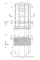
図2(a)は、第1の実施の形態に係るSAW素子の概略平面図を示し、図2(b)は、A-A’位置における概略の縦断側面図を示している。
図1(b)を用いて説明した、「交差領域ZABにおけるSAWの伝播速度よりも、バスバー領域SBにおけるSAWの伝播速度が高速とする」手法の1つ目として、本例のSAW素子は、電極指3a、3bを構成する金属膜の厚さよりも、バスバー2a、2bを構成する金属膜の厚さを薄くしている(図2(b))。
また、2つ目の手法として、電極指3a、3bを構成する金属膜の密度よりも、バスバー2a、2bを構成する金属膜の密度が小さくなるように、これらの金属膜の材料を選定している。
FIG. 2(a) shows a schematic plan view of the SAW element according to the first embodiment, and FIG. 2(b) shows a schematic vertical cross-sectional view taken along line AA'.
As a first method of "making the SAW propagation speed in the busbar region SB faster than the SAW propagation speed in the intersection region ZAB" described with reference to FIG. The metal films forming the
As a second method, materials for these metal films are selected so that the density of the metal films forming the
2つ目の手法の具体例から説明すると、バスバー2a、2bを構成する金属としてアルミニウム(Al)を選択したとき、電極指3a、3bを構成する金属としては、プラチナ(Pt)、銅(Cu)、金(Au)、銀(Ag)、タングステン(W)、モリブデン(Mo)、コバルト(Co)、鉄(Fe)、ニッケル(Ni)、クロム(Cr)、タンタル(Ta)を選択する場合を例示することができる。
なお、バスバー2a、2b及び電極指3a、3bを各々構成する金属は、上述の組み合わせ例に限定されるものではなく、他の組み合わせにより、電極指3a、3bよりも、バスバー2a、2bを構成する金属膜の密度が小さくなるようにしてもよい。
Starting with a specific example of the second technique, when aluminum (Al) is selected as the metal forming the
The metals forming the
1つ目の手法の具体例としては、図2(b)に示すように厚さの異なる金属膜からなるバスバー2a、2bと、電極指3a、3bとを別々に成膜する場合を例示することができる。
図2(b)に示す例の製造法について説明すると、圧電基板11の上面に、アルミニウムからなる所定の膜厚の金属膜を成膜した後、エッチングなどによりバスバー2a、2bをパターニングする。次いで、バスバー2a、2bがパターニングされた圧電基板11の上面に、前記アルミニウムの金属膜よりも膜厚の厚い銅の金属膜を成膜する。そして、エッチングなどにより電極指3a、3bをパターニングする。これにより、電極指3a、3bよりも、バスバー2a、2bを構成する金属膜の膜厚を薄くすることができる。
As a specific example of the first method, as shown in FIG. 2B,
2B will be described. After forming a metal film made of aluminum to a predetermined thickness on the upper surface of the
なお、上述の2つの手法を同時に採用することは必須の要件ではなく、共通の金属を用いて膜厚のみを変化させたバスバー2a、2b、電極指3a、3bを形成してもよい。バスバー2a、2b、電極指3a、3bの双方を銅により形成し、電極指3a、3bの膜厚をバスバー2a、2bの膜厚よりも厚くする場合を例示できる。
または、密度が異なる金属を用いて、共通の膜厚のバスバー2a、2b、電極指3a、3bを形成してもよい。バスバー2a、2bをアルミニウムにより形成し、電極指3a、3bを銅により形成しつつ、電極指3a、3b及びバスバー2a、2bの膜厚を揃える場合を例示できる。
It should be noted that it is not an essential requirement to employ the two methods described above at the same time, and the
Alternatively, metals having different densities may be used to form
さらに本例のSAW素子は、圧電基板11を構成する圧電材料の温度-周波数特性の影響を補償する温度補償機能を備えたTC(Temperature Compensate)-SAW素子として構成されている。
図2(b)に示すように、TC-SAW素子においては、IDT電極(バスバー2a、2b、電極指3a、3b)が形成された圧電基板11の上面に、誘電体膜5が形成(以下、「装荷」ともいう)されている。なお、図示内容が煩雑になることを避けるため、平面図である図2(a)~図8(a)においては、誘電体膜5の記載を省略(誘電体膜5の下面側を透視した状態を記載)してある。
Furthermore, the SAW element of this example is configured as a TC (Temperature Compensate)-SAW element having a temperature compensation function for compensating for the influence of the temperature-frequency characteristics of the piezoelectric material forming the
As shown in FIG. 2B, in the TC-SAW element, a dielectric film 5 (hereinafter , also called “loading”). In order to avoid complicating the illustration, the
TC-SAW素子に装荷される誘電体膜5は、圧電基板11の圧電材料とは反対の周波数温度特性を有するものが用いられる。例えば圧電基板11の圧電材料が、温度の上昇に伴って励振される周波数が低下する負の周波数温度特性を有している場合には、温度の上昇に伴って周波数が上昇する正の周波数温度特性を有する誘電体膜5が装荷される。反対に正の周波数温度特性を有する圧電材料からなる圧電基板11に対しては、負の周波数温度特性を有する誘電体膜5が装荷される。このように、圧電基板11とは反対の周波数温度特性を持つ誘電体膜5を装荷することにより、SAW素子の周囲の温度変化の影響を低減することができる。
The
例えば既述のLiNbO3は負の周波数温度特性を有する。そこで、LiNbO3により構成された圧電基板11に対しては、正の周波数温度特性を有する二酸化ケイ素、酸窒化ケイ素(化学量論比に特段の限定はなく、SiNOであってもよいし、SiO2に窒素をドープしたものであってもよい)やフッ素をドープした二酸化ケイ素の誘電体膜5を装荷する場合を例示することができる。これらの材料からなる誘電体膜5は、CVD(Chemical Vapor Deposition)やスパッタリングなどの手法によって装荷することができる。
For example, LiNbO 3 already mentioned has a negative frequency-temperature characteristic. Therefore, for the
さらに、本例のSAW素子は、図2(a)、(b)に示すように、前述の誘電体膜5のさらに上面側に、質量負荷効果によりエッジ領域EB及びギャップ領域RBのSAWの伝播速度を低下させるための伝播速度調節膜4が形成されている。
質量負荷効果を得ることを目的として形成される伝播速度調節膜4の構成材料に特段の限定はないが、成膜のしやすさや比重の大きさなどを考慮して、金属や誘電体が選択される。本例のSAW素子は、比較的成膜がしやすく比重の大きなチタン(Ti)を伝播速度調節膜4としている。この他、エッジ領域EBのSAWの伝播速度を低下させる手法として、エッジ領域EB内に位置する電極指3a、3bに拡幅部を形成してもよい。
Furthermore, as shown in FIGS. 2A and 2B, the SAW element of this example has the SAW propagation in the edge region EB and the gap region RB due to the mass load effect on the upper surface side of the
Although there is no particular limitation on the constituent material of the propagation
その他のSAW素子の概略の設計変数を示しておくと、SAW素子の設計周波数に対応する波長λに対し、電極指3a、3bの中心線間の距離dは、λ/2に設定される。また、小型のSAW素子を構成する観点では、ギャップ領域RBの幅寸法は、0.1d~2d(0.05λ~1λ)、好適には0.4d~1d(0.2λ~0.5λ)程度に設定される。
Other general design variables of the SAW element are as follows: the distance d between the center lines of the
以上に説明した構成のSAW素子によれば、図2(c)に示すSAWの伝播速度の分布図を形成することができるので、ピストンモードのSAWを励振することが可能となる。
上述の構成を備えるSAW素子において、設計周波数の周波数信号が印加されると、ピストンモードのSAWが励振されQ値が高くスプリアスの少ない周波数応答を得ることができる。
According to the SAW element having the configuration described above, it is possible to form the SAW propagation velocity distribution diagram shown in FIG.
When a frequency signal of the design frequency is applied to the SAW element having the above configuration, the piston-mode SAW is excited and a frequency response with a high Q value and little spurious can be obtained.
本実施の形態のSAW素子によれば以下の効果がある。一対のIDT電極の電極指3a、3bが交差する交差領域ZABにおけるSAWの伝播速度よりも、バスバー2a、2bが設けられたバスバー領域SBにおけるSAWの伝播速度を高速としているので、従来のIDT電極に新たな領域を追加することなくピストンモードの弾性表面波を励振することができる。
The SAW device of this embodiment has the following effects. Since the SAW propagation speed in the busbar region SB in which the
ここで、「交差領域ZABにおけるSAWの伝播速度よりも、バスバー領域SBにおけるSAWの伝播速度が高速とする」手法は、既述のバスバー2a、2b及び電極指3a、3bを構成する金属膜の膜厚を相違させることや、密度の異なる金属膜の材料を選定することに限定されない。
図3に示すSAW素子には、例えば圧電基板11に成膜された銅の金属膜をパターニングすることにより、同じ膜厚のバスバー2a、2b及び電極指3a、3bが形成されている。
Here, the technique of "making the SAW propagation speed in the busbar region SB faster than the SAW propagation speed in the crossing region ZAB" is based on the above-described metal films forming the
In the SAW element shown in FIG. 3,
一方、バスバー2a、2bの上面(電極指領域の外側)に、二酸化ケイ素やフッ素をドープした二酸化ケイ素からなる誘電体膜5よりもSAWの伝播速度が速い高速誘電体膜51を装荷している。上面側に高速誘電体膜51が装荷されたバスバー領域SBにおいては、誘電体膜5が装荷された他の領域と比較して、SAWの伝播速度が高速になることを把握している。
高速誘電体膜51を構成する誘電体としては、窒化アルミニウム(AlN)や酸化アルミニウム(Al2O3)、窒化ケイ素(SiN)を例示することができる。
On the other hand, on the upper surfaces of the
Examples of dielectrics forming the high-
また図4に示すSAW素子のように、バスバー2a、2b(バスバー領域SB)の上面側に装荷された誘電体膜5の膜厚が、他の領域(電極指領域)に装荷された誘電体膜5の膜厚よりも薄い薄化領域52を形成してもよい。SAWの伝播速度は、上面側に装荷された誘電体膜5の膜厚を薄くするに連れて高速になる。従って、薄化領域52上が形成されたバスバー領域SBにおいては、当該薄化領域52よりも厚い誘電体膜5が装荷された他の領域と比較して、SAWの伝播速度が高速になる。
薄化領域52は、例えばSAW素子の全面に、均一な膜厚の誘電体膜5を装荷した後、バスバー領域SBの上面側の誘電体膜5の一部をエッチングにて削り取ることなどにより、形成することができる。
Further, like the SAW element shown in FIG. 4, the thickness of the
The thinned
また、バスバー2a、2bの上面側(バスバー領域SB、即ち、電極指領域の外側)には、誘電体膜5を装荷しないことにより、誘電体膜5が装荷された他の領域と比較してSAWの伝播速度を高速にすることもできる(図示省略)。
以上に説明した各種の実施の形態におけるSAWの伝播速度の調節手法は、図2を用いて説明した、既述のバスバー2a、2b及び電極指3a、3bを構成する金属膜の膜厚、密度が異なるSAW素子にも組み合わせて適用することができる。
In addition, by not loading the
The method of adjusting the SAW propagation speed in the various embodiments described above is based on the film thickness, density can be applied in combination to SAW elements having different characteristics.
次いで、図5~図8を参照しながら、エッジ領域EBにおけるSAWの伝播速度を低下させる手法の変形例について説明する。
ここで、これら図5~図8に示すSAW素子には、複数のダミー電極31a、31bが形成されている。ダミー電極31a、31bは、一方のバスバー2a、2bに接続された複数の電極指3a、3bの先端部と、他方のバスバー2b、2aとの間に、これらの先端部から離れて、他方のバスバー2b、2aから伸び出すように形成されている。
Next, modified examples of the method for reducing the SAW propagation speed in the edge region EB will be described with reference to FIGS. 5 to 8. FIG.
A plurality of
ダミー電極31a、31bは、SAW素子の周波数特性におけるスプリアスの発生を抑制する効果がある。従って、図2~図4を用いて説明した各SAW素子においても、ダミー電極31a、31bを形成してもよい。
ダミー電極31a、31bが形成されたダミー領域の幅寸法は、0.2d~1d(0.1λ~0.5λ)程度に設定される。
The
The width dimension of the dummy region in which the
図5に示すSAW素子は、図4に示した帯状の伝播速度調節膜4に替えて、電極指3a、3bのエッジ領域EBに含まれる部分、及び電極指3a、3b、ダミー電極31a、31bのダミー領域DBに含まれる部分に、グレーティング状に伝播速度調節膜41を形成した例を示している。
In the SAW element shown in FIG. 5, instead of the strip-shaped propagation
また図6に示すSAW素子は、図4に示した帯状の伝播速度調節膜4に替えて、電極指3a、3bのエッジ領域EBに含まれる部分であって、電極指3a、3bの上面側に、グレーティング状に例えば銅からなる伝播速度調節膜41を形成した例を示している。従って、本例のSAW素子においては、伝播速度調節膜41の上面側に誘電体膜5が装荷されている。
In the SAW element shown in FIG. 6, instead of the strip-shaped propagation
図6において、図示の便宜上、誘電体膜5の膜厚は成膜位置に応じて変化しているように記載されているが、CVDやスパッタリングリングなどの手法によって装荷された誘電体膜5は下部側の構造物(バスバー2a、2b、電極指3a、3b、伝播速度調節膜41)の段差形状に沿って、ほぼ一定の膜厚の誘電体膜5が形成される。従って、伝播速度調節膜41の下部側のエッジ領域EBにおいては、誘電体膜5の装荷に伴う質量負荷効果に加えて、伝播速度調節膜41の装荷に伴う質量負荷効果により、他の領域よりもSAWの伝播速度を低下させることができる(図7、図8に示すSAW素子の例において同じ)。
In FIG. 6, for convenience of illustration, the film thickness of the
次いで図7に示すSAW素子は、電極指3a、3bの基端部の下面側であって、エッジ領域EBの下面側に至る領域に向けて、バスバー2a、2bから電極指状に伸びる伝播速度調節膜41’を形成し、また電極指3a、3bの先端部の下面側にアルミニウムの伝播速度調節膜41を形成した例を示している。これら伝播速度調節膜41’、41を装荷することにより、エッジ領域EBにおけるSAWの伝播速度を低下させることもできる。
また図7に示すSAW素子の変形例として、図8に示すSAW素子のように、電極指3a、3bの先端部の下面側の伝播速度調節膜41の形成は省略してもよい。
Next, in the SAW element shown in FIG. 7, the propagation speed of the
As a modification of the SAW element shown in FIG. 7, like the SAW element shown in FIG. 8, the formation of the propagation
さらには、ピストンモードを励振するSAW素子は、誘電体膜5が装荷されたTC-SAW素子でなくてもよい。この場合、図2~図3に示すように電極指3a、3b間を跨る伝播速度調節膜4を形成する場合には、短絡防止の観点から、例えば誘電体により伝播速度調節膜4を形成してもよい。またこのとき、伝播速度調節膜4、41は、酸化テルルのように、SAWの伝播速度が低い誘電体を採用してもよい。
Furthermore, the SAW element that excites the piston mode does not have to be the TC-SAW element loaded with the
また温度変化に伴う膨張・伸縮の影響を抑制するため、圧電基板11の底面側に熱膨張率の小さい支持基板を貼り合わせてもよい。支持基板としてはシリコン(Si)、水晶(SiO2)、ガラス、ダイヤモンド(C)、サファイア(Al2O3)を例示することができる.さらに支持基板と圧電基板11との間に誘電体層(例えば二酸化ケイ素)や金属層を形成してもよい。
Further, in order to suppress the influence of expansion and contraction due to temperature change, a support substrate having a small coefficient of thermal expansion may be attached to the bottom surface of the
さらにまた、SAW素子に耐候性を持たせるため、あるいはSAW素子の周波数調整(トリミング)を行うために、SAW素子の最上層に上層膜を形成してもよい。上層膜は、IDT電極(バスバー2a、2b、電極指3a、3b、ダミー電極31a、31b)や伝播速度調節膜4、41、41’、誘電体膜5よりも上層側に形成される。上層膜は、例えば窒化ケイ素により構成することができる。
Furthermore, an upper layer film may be formed on the uppermost layer of the SAW element in order to impart weather resistance to the SAW element or to perform frequency adjustment (trimming) of the SAW element. The upper layer film is formed above the IDT electrodes (
以上に説明したSAW素子は、図2~図8に示す単体のSAW素子にて電子部品として利用することができる。また、圧電基板11を縦方向に広げ、IDT電極の前後に、グレーティング反射器を設けてもよい。
さらに当該SAW素子は、共通の圧電基板11に複数のIDT電極を設けた弾性波共振器や弾性波フィルタにも適用することができる。
The SAW element described above can be used as an electronic component as a single SAW element shown in FIGS. Alternatively, the
Furthermore, the SAW element can also be applied to elastic wave resonators and elastic wave filters in which a plurality of IDT electrodes are provided on a common
そしてフィルタ、デュプレクサ、クアッドプレクサ、その他フィルタ機能を有するデバイスに本例のSAW素子は用いることができる。また当該デバイスは、PAMiD、PAiD、PADなどと呼ばれるパワーアンプデュプレクサモジュール(Power Amp Integrated Duplexer)、DiFEMなどと呼ばれるダイバーシティ受信用モジュール(Diversity Front End Module)に組み込むことができる。 The SAW element of this example can be used for filters, duplexers, quadplexers, and other devices having filter functions. The device can also be incorporated into a Power Amp Integrated Duplexer module called PAMiD, PAiD, PAD, etc., or a Diversity Front End Module called DiFEM.
SAWの伝播速度分布に応じたSAW素子の周波数特性をシミュレーションにより確認した。
A.シミュレーション条件
(実施例)
図2(c)に示すSAWの伝播速度分布を有するSAW素子のシミュレーションモデルを作成し、周波数-アドミタンス特性を調べた。その結果を図10に示す。
(比較例)
図9に示すように、交差領域ZABにおけるSAWの伝播速度よりも、バスバー領域SBにおけるSAWの伝播速度が低速であるSAWの伝播速度分布を有するSAW素子のシミュレーションモデルを作成し、周波数-アドミタンス特性を調べた。その結果を図11に示す。
The frequency characteristics of the SAW element according to the SAW propagation velocity distribution were confirmed by simulation.
A. Simulation conditions (example)
A simulation model of a SAW element having the SAW propagation velocity distribution shown in FIG. 2(c) was prepared to examine frequency-admittance characteristics. The results are shown in FIG.
(Comparative example)
As shown in FIG. 9, a simulation model of a SAW element having a SAW propagation velocity distribution in which the SAW propagation velocity in the busbar area SB is slower than the SAW propagation velocity in the crossing area ZAB was created, and the frequency-admittance characteristics examined. The results are shown in FIG.
B.シミュレーション結果
図10に示す実施例のシミュレーション結果によれば、SAWの共振点、反共振点が確認され、SAW素子として利用可能な特性を備えていることが確認できた。また、高次の横モードに起因するスプリアスも観察されず、挿入損失の小さいSAW素子を構成することができた。
B. Simulation Results According to the simulation results of the example shown in FIG. 10, the resonance point and anti-resonance point of the SAW were confirmed, and it was confirmed that the SAW device has characteristics that can be used as a SAW element. Moreover, no spurious due to high-order transverse modes was observed, and a SAW element with small insertion loss could be constructed.
一方、図11に示すように、比較例に係るSAW素子においては、高次の横モードに起因する多数のスプリアスが確認され、実施例のSAW素子と比べて挿入損失が大きくなることが分かる。
このように、実施例と比較例の対比からも、伝播速度調節膜4を備えた実施例に係るSAW素子は、スプリアスの少ない良好な特性を有することが確認された。
On the other hand, as shown in FIG. 11, in the SAW element according to the comparative example, many spurious emissions caused by higher-order transverse modes are confirmed, and it can be seen that the insertion loss is larger than that of the SAW element according to the example.
As described above, it was confirmed from the comparison between the example and the comparative example that the SAW element according to the example provided with the propagation
ZAB 交差領域
SB バスバー領域
11 圧電基板
2a、2b バスバー
3a、3b 電極指
31a、31b
ダミー電極
4、41、41’
伝播速度調節膜
ZAB Intersection area
Propagation velocity control membrane
Claims (14)
前記圧電基板上に形成された一対のバスバーと、これらバスバーの各々から対向するバスバーに向かって互いに櫛歯状に伸び出す複数の電極指と、を備え、これら複数の電極指の並び方向に沿って見たとき、一方のバスバーに接続された電極指と、他方のバスバーに接続された電極指とが交差する領域である交差領域が形成された一対のIDT電極と、を備え、
前記交差領域の端部側の領域であって、前記複数の電極指の先端部を含み、前記バスバーに沿って伸びる帯状の領域をエッジ領域と呼ぶとき、前記エッジ領域での弾性表面波の伝播速度が、前記交差領域での弾性表面波の伝播速度より低速であることと、
前記交差領域における弾性表面波の伝播速度よりも、前記バスバーが設けられた領域であるバスバー領域における弾性表面波の伝播速度が高速であることと、
前記一対のバスバーの各々について、一方のバスバーに接続された複数の電極指の先端部と、他方のバスバーとの間に、これらの先端部から離れて、他方のバスバーから伸び出す複数のダミー電極が形成され、前記ダミー電極を含み、前記バスバーに沿って伸びる帯状の領域であるダミー電極領域における弾性表面波の伝播速度が、前記エッジ領域での弾性表面波の伝播速度よりも高速、且つ、前記バスバー領域での弾性表面波の伝播速度よりも低速であり、さらに、前記エッジ領域と前記ダミー電極領域とに挟まれたギャップ領域では、弾性表面波の伝播速度が、前記バスバー領域での弾性表面波の伝播速度よりも高速であることを特徴とする弾性表面波素子。 a piezoelectric substrate;
a pair of busbars formed on the piezoelectric substrate; and a plurality of electrode fingers extending from each of the busbars toward the opposing busbars in a comb-teeth shape; When viewed from above, a pair of IDT electrodes in which an intersection region is formed where an electrode finger connected to one bus bar and an electrode finger connected to the other bus bar intersect,
When a band-like region extending along the bus bar, which is a region on the end side of the intersection region and includes the tips of the plurality of electrode fingers, is called an edge region, surface acoustic waves propagate in the edge region. the velocity is lower than the propagation velocity of surface acoustic waves in the intersection region;
The propagation speed of the surface acoustic waves in the busbar region, which is the region where the busbars are provided, is higher than the propagation speed of the surface acoustic waves in the intersection region;
For each of the pair of busbars, a plurality of dummy electrodes extending from the other busbar away from the tips of the plurality of electrode fingers connected to one busbar and the other busbar. is formed, and the surface acoustic wave propagation speed in the dummy electrode region, which is a strip-shaped region that includes the dummy electrode and extends along the bus bar, is higher than the propagation speed of the surface acoustic wave in the edge region, and The propagation speed of the surface acoustic wave is lower than that in the busbar region, and furthermore, in the gap region sandwiched between the edge region and the dummy electrode region, the propagation speed of the surface acoustic wave is lower than that of the elastic surface wave in the busbar region. A surface acoustic wave device characterized by having a propagation speed higher than that of a surface wave.
Priority Applications (5)
| Application Number | Priority Date | Filing Date | Title |
|---|---|---|---|
| JP2018215986A JP7178881B2 (en) | 2018-11-16 | 2018-11-16 | surface acoustic wave element |
| CN201911104936.8A CN111200415A (en) | 2018-11-16 | 2019-11-13 | Surface acoustic wave device |
| TW108141644A TWI762832B (en) | 2018-11-16 | 2019-11-15 | Surface acoustic wave device |
| US16/684,607 US11683019B2 (en) | 2018-11-16 | 2019-11-15 | Surface acoustic wave device |
| JP2022104962A JP7377920B2 (en) | 2018-11-16 | 2022-06-29 | surface acoustic wave device |
Applications Claiming Priority (1)
| Application Number | Priority Date | Filing Date | Title |
|---|---|---|---|
| JP2018215986A JP7178881B2 (en) | 2018-11-16 | 2018-11-16 | surface acoustic wave element |
Related Child Applications (1)
| Application Number | Title | Priority Date | Filing Date |
|---|---|---|---|
| JP2022104962A Division JP7377920B2 (en) | 2018-11-16 | 2022-06-29 | surface acoustic wave device |
Publications (2)
| Publication Number | Publication Date |
|---|---|
| JP2020088459A JP2020088459A (en) | 2020-06-04 |
| JP7178881B2 true JP7178881B2 (en) | 2022-11-28 |
Family
ID=70726931
Family Applications (2)
| Application Number | Title | Priority Date | Filing Date |
|---|---|---|---|
| JP2018215986A Active JP7178881B2 (en) | 2018-11-16 | 2018-11-16 | surface acoustic wave element |
| JP2022104962A Active JP7377920B2 (en) | 2018-11-16 | 2022-06-29 | surface acoustic wave device |
Family Applications After (1)
| Application Number | Title | Priority Date | Filing Date |
|---|---|---|---|
| JP2022104962A Active JP7377920B2 (en) | 2018-11-16 | 2022-06-29 | surface acoustic wave device |
Country Status (4)
| Country | Link |
|---|---|
| US (1) | US11683019B2 (en) |
| JP (2) | JP7178881B2 (en) |
| CN (1) | CN111200415A (en) |
| TW (1) | TWI762832B (en) |
Families Citing this family (14)
| Publication number | Priority date | Publication date | Assignee | Title |
|---|---|---|---|---|
| JP2020145567A (en) * | 2019-03-06 | 2020-09-10 | 株式会社村田製作所 | Acoustic wave device |
| US11652466B2 (en) * | 2019-08-29 | 2023-05-16 | Skyworks Solutions, Inc. | Suppression of transverse mode spurious signals in surface acoustic wave devices utilizing a dense film above gap region of interdigital transducer electrodes |
| US11705883B2 (en) * | 2019-10-24 | 2023-07-18 | Skyworks Solutions, Inc. | Acoustic wave resonator with mass loading strip for suppression of transverse mode |
| US11936367B2 (en) * | 2019-10-31 | 2024-03-19 | Skyworks Solutions, Inc. | Acoustic wave device with velocity reduction cover |
| US20210344322A1 (en) * | 2020-04-30 | 2021-11-04 | RF360 Europe GmbH | Surface acoustic wave electroacoustic device for reduced transversal modes |
| JP2022011770A (en) * | 2020-06-30 | 2022-01-17 | NDK SAW devices株式会社 | Surface acoustic wave element |
| US11405017B2 (en) | 2020-10-05 | 2022-08-02 | Resonant Inc. | Acoustic matrix filters and radios using acoustic matrix filters |
| US20220352867A1 (en) * | 2021-04-30 | 2022-11-03 | Resonant Inc. | Transversely-excited film bulk acoustic resonator with oxide strip acoustic confinement structures |
| CN113839648B (en) * | 2021-09-14 | 2023-08-29 | 常州承芯半导体有限公司 | Surface acoustic wave resonator device, surface acoustic wave resonator forming method, filter device and radio frequency front-end device |
| TWI789913B (en) * | 2021-09-16 | 2023-01-11 | 台灣嘉碩科技股份有限公司 | Surface acoustic wave resonator and filter utilizing effective reflection structure |
| WO2024043342A1 (en) * | 2022-08-26 | 2024-02-29 | 株式会社村田製作所 | Elastic wave device |
| WO2024043346A1 (en) * | 2022-08-26 | 2024-02-29 | 株式会社村田製作所 | Acoustic wave device |
| CN115473506B (en) * | 2022-09-16 | 2023-08-22 | 南通大学 | Method for reducing volume of surface acoustic wave device |
| CN116208115A (en) * | 2023-02-07 | 2023-06-02 | 锐石创芯(重庆)科技有限公司 | Elastic wave device, method for manufacturing elastic wave device, filter, and electronic apparatus |
Citations (6)
| Publication number | Priority date | Publication date | Assignee | Title |
|---|---|---|---|---|
| JP2003087083A (en) | 2001-07-04 | 2003-03-20 | Murata Mfg Co Ltd | Comb type electrode section, surface acoustic wave device and communications equipment for surface acoustic wave |
| JP2009159039A (en) | 2007-12-25 | 2009-07-16 | Panasonic Corp | Elastic boundary wave device, and filter and antenna duplexer using the same |
| WO2009147787A1 (en) | 2008-06-06 | 2009-12-10 | パナソニック株式会社 | Acoustic wave duplexer |
| JP2016184951A (en) | 2011-03-25 | 2016-10-20 | スカイワークスフィルターソリューションズジャパン株式会社 | Acoustic wave device with suppressed higher order transverse mode |
| JP2017112603A (en) | 2015-12-14 | 2017-06-22 | 太陽誘電株式会社 | Acoustic wave resonator, filter and duplexer |
| WO2018003282A1 (en) | 2016-06-28 | 2018-01-04 | 株式会社村田製作所 | Elastic wave device |
Family Cites Families (19)
| Publication number | Priority date | Publication date | Assignee | Title |
|---|---|---|---|---|
| JPS5221616U (en) | 1975-08-04 | 1977-02-16 | ||
| JPS553020U (en) | 1978-06-22 | 1980-01-10 | ||
| JP3412611B2 (en) | 2000-09-25 | 2003-06-03 | 株式会社村田製作所 | Surface acoustic wave device |
| JP3498215B2 (en) * | 2001-04-09 | 2004-02-16 | 株式会社村田製作所 | Surface acoustic wave filter, surface acoustic wave device, and communication device |
| JP3929415B2 (en) | 2003-04-23 | 2007-06-13 | 富士通メディアデバイス株式会社 | Surface acoustic wave device |
| JP4465625B2 (en) * | 2006-09-29 | 2010-05-19 | Tdk株式会社 | Surface acoustic wave filter and surface acoustic wave resonator |
| JP2009077209A (en) * | 2007-09-21 | 2009-04-09 | Seiko Epson Corp | Surface acoustic wave resonator |
| US7576471B1 (en) * | 2007-09-28 | 2009-08-18 | Triquint Semiconductor, Inc. | SAW filter operable in a piston mode |
| US7939989B2 (en) | 2009-09-22 | 2011-05-10 | Triquint Semiconductor, Inc. | Piston mode acoustic wave device and method providing a high coupling factor |
| DE102010005596B4 (en) | 2010-01-25 | 2015-11-05 | Epcos Ag | Electroacoustic transducer with reduced losses due to transversal emission and improved performance by suppression of transverse modes |
| JP2012227626A (en) * | 2011-04-15 | 2012-11-15 | Panasonic Corp | Surface acoustic wave element |
| JP5797979B2 (en) * | 2011-08-31 | 2015-10-21 | 太陽誘電株式会社 | Elastic wave device |
| WO2014192756A1 (en) * | 2013-05-29 | 2014-12-04 | 株式会社村田製作所 | Acoustic wave device |
| KR20170034939A (en) * | 2013-05-29 | 2017-03-29 | 가부시키가이샤 무라타 세이사쿠쇼 | Elastic wave filter device |
| JP6494447B2 (en) | 2015-01-20 | 2019-04-03 | 太陽誘電株式会社 | Elastic wave device |
| FR3042648B1 (en) * | 2015-10-20 | 2018-09-07 | Soitec Silicon On Insulator | SURFACE ACOUSTIC WAVE DEVICE AND METHOD OF MANUFACTURING THE SAME |
| JP6415469B2 (en) | 2016-03-22 | 2018-10-31 | 太陽誘電株式会社 | Acoustic wave resonator, filter and multiplexer, and method for manufacturing acoustic wave resonator |
| JP6465065B2 (en) * | 2016-04-25 | 2019-02-06 | 株式会社村田製作所 | Elastic wave device |
| JP6954799B2 (en) * | 2017-10-20 | 2021-10-27 | 株式会社村田製作所 | Elastic wave device |
-
2018
- 2018-11-16 JP JP2018215986A patent/JP7178881B2/en active Active
-
2019
- 2019-11-13 CN CN201911104936.8A patent/CN111200415A/en active Pending
- 2019-11-15 US US16/684,607 patent/US11683019B2/en active Active
- 2019-11-15 TW TW108141644A patent/TWI762832B/en active
-
2022
- 2022-06-29 JP JP2022104962A patent/JP7377920B2/en active Active
Patent Citations (6)
| Publication number | Priority date | Publication date | Assignee | Title |
|---|---|---|---|---|
| JP2003087083A (en) | 2001-07-04 | 2003-03-20 | Murata Mfg Co Ltd | Comb type electrode section, surface acoustic wave device and communications equipment for surface acoustic wave |
| JP2009159039A (en) | 2007-12-25 | 2009-07-16 | Panasonic Corp | Elastic boundary wave device, and filter and antenna duplexer using the same |
| WO2009147787A1 (en) | 2008-06-06 | 2009-12-10 | パナソニック株式会社 | Acoustic wave duplexer |
| JP2016184951A (en) | 2011-03-25 | 2016-10-20 | スカイワークスフィルターソリューションズジャパン株式会社 | Acoustic wave device with suppressed higher order transverse mode |
| JP2017112603A (en) | 2015-12-14 | 2017-06-22 | 太陽誘電株式会社 | Acoustic wave resonator, filter and duplexer |
| WO2018003282A1 (en) | 2016-06-28 | 2018-01-04 | 株式会社村田製作所 | Elastic wave device |
Also Published As
| Publication number | Publication date |
|---|---|
| US20200162052A1 (en) | 2020-05-21 |
| JP2022126852A (en) | 2022-08-30 |
| JP7377920B2 (en) | 2023-11-10 |
| TWI762832B (en) | 2022-05-01 |
| TW202021271A (en) | 2020-06-01 |
| JP2020088459A (en) | 2020-06-04 |
| US11683019B2 (en) | 2023-06-20 |
| CN111200415A (en) | 2020-05-26 |
Similar Documents
| Publication | Publication Date | Title |
|---|---|---|
| JP7178881B2 (en) | surface acoustic wave element | |
| KR102479702B1 (en) | elastic wave device | |
| US7528685B2 (en) | Lamb wave type high frequency device | |
| KR20190110020A (en) | Elastic wave device | |
| KR102140089B1 (en) | Acoustic wave resonator, filter, and multiplexer | |
| JP2014187568A (en) | Acoustic wave device | |
| US20220216846A1 (en) | Acoustic wave device | |
| US20220014175A1 (en) | Acoustic wave device | |
| JP5338914B2 (en) | Elastic wave device, duplexer and electronic device using the same | |
| JP2022011770A (en) | Surface acoustic wave element | |
| JP2020188408A (en) | Surface acoustic wave device, filter circuit, and electronic component | |
| JPWO2005086345A1 (en) | Boundary acoustic wave device | |
| US11936359B2 (en) | Acoustic wave device and multiplexer | |
| US20220216848A1 (en) | Acoustic wave device | |
| JP5083469B2 (en) | Surface acoustic wave device | |
| CN113519120B (en) | Elastic wave device | |
| US20220224305A1 (en) | Acoustic wave device | |
| JP7203578B2 (en) | surface acoustic wave element | |
| KR102629355B1 (en) | elastic wave device | |
| JPWO2005036744A1 (en) | Boundary acoustic wave device | |
| JP2022171054A (en) | Acoustic wave resonator, filter, and multiplexer | |
| JP2006270360A (en) | Surface acoustic wave element | |
| WO2024004862A1 (en) | Filter device and communication device | |
| JP2022178244A (en) | Acoustic wave device, filter, multiplexer and method for manufacturing acoustic wave device | |
| JP2008017249A (en) | Surface acoustic wave device piece and surface acoustic wave device |
Legal Events
| Date | Code | Title | Description |
|---|---|---|---|
| A711 | Notification of change in applicant |
Free format text: JAPANESE INTERMEDIATE CODE: A712 Effective date: 20200925 |
|
| A521 | Request for written amendment filed |
Free format text: JAPANESE INTERMEDIATE CODE: A523 Effective date: 20201006 |
|
| A621 | Written request for application examination |
Free format text: JAPANESE INTERMEDIATE CODE: A621 Effective date: 20210519 |
|
| A977 | Report on retrieval |
Free format text: JAPANESE INTERMEDIATE CODE: A971007 Effective date: 20220218 |
|
| A131 | Notification of reasons for refusal |
Free format text: JAPANESE INTERMEDIATE CODE: A131 Effective date: 20220301 |
|
| A601 | Written request for extension of time |
Free format text: JAPANESE INTERMEDIATE CODE: A601 Effective date: 20220425 |
|
| A521 | Request for written amendment filed |
Free format text: JAPANESE INTERMEDIATE CODE: A523 Effective date: 20220629 |
|
| A131 | Notification of reasons for refusal |
Free format text: JAPANESE INTERMEDIATE CODE: A131 Effective date: 20220726 |
|
| A521 | Request for written amendment filed |
Free format text: JAPANESE INTERMEDIATE CODE: A523 Effective date: 20220920 |
|
| TRDD | Decision of grant or rejection written | ||
| A01 | Written decision to grant a patent or to grant a registration (utility model) |
Free format text: JAPANESE INTERMEDIATE CODE: A01 Effective date: 20221108 |
|
| A61 | First payment of annual fees (during grant procedure) |
Free format text: JAPANESE INTERMEDIATE CODE: A61 Effective date: 20221115 |
|
| R150 | Certificate of patent or registration of utility model |
Ref document number: 7178881 Country of ref document: JP Free format text: JAPANESE INTERMEDIATE CODE: R150 |