EP1471618A2 - Voltage equalizer for capacitors - Google Patents
Voltage equalizer for capacitors Download PDFInfo
- Publication number
- EP1471618A2 EP1471618A2 EP04009698A EP04009698A EP1471618A2 EP 1471618 A2 EP1471618 A2 EP 1471618A2 EP 04009698 A EP04009698 A EP 04009698A EP 04009698 A EP04009698 A EP 04009698A EP 1471618 A2 EP1471618 A2 EP 1471618A2
- Authority
- EP
- European Patent Office
- Prior art keywords
- capacitors
- coils
- switching elements
- voltage equalizer
- blocks
- Prior art date
- Legal status (The legal status is an assumption and is not a legal conclusion. Google has not performed a legal analysis and makes no representation as to the accuracy of the status listed.)
- Withdrawn
Links
Images

Classifications
-
- H—ELECTRICITY
- H02—GENERATION; CONVERSION OR DISTRIBUTION OF ELECTRIC POWER
- H02M—APPARATUS FOR CONVERSION BETWEEN AC AND AC, BETWEEN AC AND DC, OR BETWEEN DC AND DC, AND FOR USE WITH MAINS OR SIMILAR POWER SUPPLY SYSTEMS; CONVERSION OF DC OR AC INPUT POWER INTO SURGE OUTPUT POWER; CONTROL OR REGULATION THEREOF
- H02M3/00—Conversion of DC power input into DC power output
- H02M3/22—Conversion of DC power input into DC power output with intermediate conversion into AC
- H02M3/24—Conversion of DC power input into DC power output with intermediate conversion into AC by static converters
- H02M3/28—Conversion of DC power input into DC power output with intermediate conversion into AC by static converters using discharge tubes with control electrode or semiconductor devices with control electrode to produce the intermediate AC
- H02M3/325—Conversion of DC power input into DC power output with intermediate conversion into AC by static converters using discharge tubes with control electrode or semiconductor devices with control electrode to produce the intermediate AC using devices of a triode or a transistor type requiring continuous application of a control signal
- H02M3/335—Conversion of DC power input into DC power output with intermediate conversion into AC by static converters using discharge tubes with control electrode or semiconductor devices with control electrode to produce the intermediate AC using devices of a triode or a transistor type requiring continuous application of a control signal using semiconductor devices only
- H02M3/33569—Conversion of DC power input into DC power output with intermediate conversion into AC by static converters using discharge tubes with control electrode or semiconductor devices with control electrode to produce the intermediate AC using devices of a triode or a transistor type requiring continuous application of a control signal using semiconductor devices only having several active switching elements
- H02M3/33576—Conversion of DC power input into DC power output with intermediate conversion into AC by static converters using discharge tubes with control electrode or semiconductor devices with control electrode to produce the intermediate AC using devices of a triode or a transistor type requiring continuous application of a control signal using semiconductor devices only having several active switching elements having at least one active switching element at the secondary side of an isolation transformer
-
- H—ELECTRICITY
- H02—GENERATION; CONVERSION OR DISTRIBUTION OF ELECTRIC POWER
- H02M—APPARATUS FOR CONVERSION BETWEEN AC AND AC, BETWEEN AC AND DC, OR BETWEEN DC AND DC, AND FOR USE WITH MAINS OR SIMILAR POWER SUPPLY SYSTEMS; CONVERSION OF DC OR AC INPUT POWER INTO SURGE OUTPUT POWER; CONTROL OR REGULATION THEREOF
- H02M1/00—Details of apparatus for conversion
- H02M1/08—Circuits specially adapted for the generation of control voltages for semiconductor devices incorporated in static converters
Definitions
- the present invention relates to a voltage equalizer for capacitors which equalizes terminal voltages of a plurality of capacitors connected in series.
- a battery including a number of capacitors connected in series is loaded into an electric vehicle which runs by a motor or a hybrid vehicle which runs by using both engine and motor.
- the battery is provided with a voltage equalizer which equalizes terminal voltages of the capacitors in consideration of securing a charging capacity, long life of each capacitor, and safety, etc.
- a voltage equalizer and a voltage equalizationmethodamong apluralityof capacitors or converters connected in series disclosed in United States Patent No. 5821729, has been known.
- the voltage equalizer a plurality of capacitors connected in series and a transformer having a plurality of coils is provided, the coils are connected to the respective capacitors via a plurality of switches, and the terminal voltages of the capacitors are equalized by switching the switches.
- An object of the present invention is to provide a voltage equalizer for capacitors which eliminates problems that cause an increase in size of the transformer or require another measure to be taken for the one-directional magnetizing force of the transformer, and to realize a cost reduction along with a reduction in the number of parts and simplification and downsizing of the voltage equalizer.
- the present invention provides a voltage equalizer 1x for capacitors which equalizes the terminal voltages Ea, Eb, Ec... of a plurality of capacitors Ba, Bb, Bc... connected in series, the voltage equalizer comprising:
- coils 2aa... can be connected in reverse in advance so that the polarities of corresponding coils 2aa... alternately reverse.
- terminal voltages of capacitors Ba... of blocks Ca... that have switching elements 3aa... which are controlled to be ON n-th are defined as E n
- the number of windings of the coils 2aa... is defined as N n
- an ON time of the switching elements 3aa... is defined as T n
- terminal voltages of the capacitors Bc... of blocks Cb... having switching elements 3ba... that are controlled to be ON n+1-th are defined as E n+1
- the control unit 4 monitors the terminal voltages Ea... of the capacitors Ba..., and when the scattering of the terminal voltages Ea... falls within a predetermined range, the control unit 4 can control to stop ON-control of the switching elements 3aa...
- each capacitor Ba... can be formed of one cell or a plurality of cells.
- the capacitors Ba... are preferably used for a battery B to be loaded into an electric vehicle which runs by a motor or a hybrid vehicle which runs by using both engine and motor.
- a plurality of modules M1, M2... each has a transformer 2 with a plurality of coils 2aa... corresponding to the respective capacitors Ba... and a plurality of switching elements 3aa... corresponding to the respective coils 2aa..., wherein the coils 2aa..., the switching elements 3aa..., and the capacitors Ba... are connected in series to each other to form a plurality of loop circuits Raa..., and the loop circuits Raa... are divided into a plurality of blocks Ca... each including an arbitrary number of loop circuits Raa....
- the capacitors Ba.- of the modules M1... are connected in series to each other, and equalizing coils 5... are provided for the transformers 2... in the modules M1... so that the equalizing coils 5 are connected in parallel to each other.
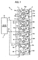
- B indicates a battery, more specifically, a battery to be loaded into an electric vehicle which runs by a motor or a hybrid vehicle which runs by using both engine and .. motor.
- the battery B is constructed by connecting a plurality of capacitors Ba, Bb, Bc... Bh in series, and for the capacitors Ba..., various capacitors including an ionbattery such as a lithium ion battery, an electric double layer capacitor, etc., can be used.
- the example shows the case where a lithium ion battery is used.
- the capacitors Ba... may be formed of one cell, or a plurality of cells, for example, a plurality of cells connected in series or parallel, or a combination of cells connected in series and parallel.
- the voltage equalizer 1x which equalizes terminal voltages Ea, Eb, Ec... Eh of the capacitors Ba, Bb, Bc... Bh is connected to the battery B,.
- the voltage equalizer 1x has a transformer 2 having an iron core, and the transformer 2 has coils 2aa, 2ab, 2ac, 2ad, 2ba, 2bb, 2bc, and 2bd as many as the capacitors Ba.... Regarding the coils 2aa, 2ab, 2ac, and 2ad that are a part (half) of all the coils 2aa...
- winding start terminals are connected to positive terminal sides of the capacitors Ba, Bb, Be, and Bf, respectively, and winding end terminals are connected to negative terminal sides of the capacitors Ba, Bb, Be, and Bf via switching elements 3aa, 3ab, 3ac, and 3ad.
- loop circuits Raa, Rab, Rac, and Rad corresponding to the respective capacitors Ba, Bb, Be, and Bf are constructed, and these loop circuits Raa... form one block, that is, a first block Ca.
- winding end terminals are connected to positive terminal sides of the capacitors Bc, Bd, Bg, and Bh, respectively, and winding start terminals are connected to negative terminal sides of the capacitors Bc, Bd, Bg, and Bh via switching elements 3ba, 3bb, 3bc, and 3bd.
- loop circuits Rba, Rbb, Rbc, and Rbd corresponding to the respective capacitors Bc, Bd, Bg, and Bh are constructed, and these loop circuits Rba... form one block, that is, a second block Cb. Therefore, the voltage equalizer 1x shown in Fig. 1 is divided into the two blocks Ca and Cb each of which includes four loop circuits Raa... and Rba....
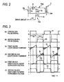
- an FET 30 shown in Fig. 2 can be used for the switching element 3aa (the same applies to other switching elements 3ab).
- a drain-source section of the FET 30 is connectedbetween the winding end terminal of the coil 2aa and the negative terminal side of the capacitor Ba.
- Cp and Dp indicate a parasitic capacitor and a parasitic diode generated inside the FET 30, respectively.
- the reference numeral 4 denotes a control unit.
- the control unit 4 has a drive circuit 10.
- the drive circuit 10 outputs pulse signals S1 and S2 with frequencies of approximately several hundred kHz oscillating from a built-in pulse oscillator.
- One pulse signal S1 is supplied to the first block Ca to control the switching elements 3aa... to be ON, and the other pulse signal S2 is supplied to the second block Cb to control the switching elements 3ba... to be ON.
- the pulse signals S1 and S2 are supplied to the respective gates of corresponding FETs 30.
- waveforms of the pulse signals S1 and S2 have phases displaced from each other by 180 degrees as shown in Fig. 3(a) and Fig. 3(b).
- the coils 2aa... and 2ba... of the first block Ca and the second block Cb are connected to the capacitors Ba... and Bc..., respectively, so that their polarities are reverse to eachother.
- the pulse signals S1 and S2 are supplied, the polarities of the coils 2aa... and 2ba... of the blocks Ca and Cb alternately reverse.
- the control unit 4 is constructed by such connection of the coils 2aa... and 2ba... in which their polarities reverse and the drive circuit 10.
- control unit 4 it is also possible that polarity switching circuits or the like are connected between the coils 2aa... and the capacitors Ba..., and switching signals are supplied from the drive circuit 10 to these polarity switching circuits or the like to make control so that the polarities of the coils 2aa... alternately reverse.
- polarity switching circuits or the like By connecting in advance the coils 2ba... so that the polarities of corresponding coils reverse to each other, the polarity switching circuits or the like become unnecessary, and this provides an advantage in which the present -invention is carried out easily at low cost.
- the abovementioned circuitry is set so that, in a case where the terminal voltages of capacitors Ba... of the first block Ca are defined as E n , the number of windings of the coils 2aa... is defined as N n , the ON time of the switching elements 3aa... is defined as T n , the terminal voltages of the capacitors Bc... of the second block Cb are defined as E n+1 , the number of windings of the coils 2ba... is defined as N n+1 , and the ON time of the switching elements 3ba...
- Fig. 3 shows time charts of signals at the respective parts of the voltage equalizer 1 shown in Fig. 1. Description is given on the assumption that the FET 30 is used for the respective switching elements 3aa....
- the switching elements 3aa... of the first block Ca are turned OFF, the switching elements 3ba... of the second block Cb are turned ON, the energy stored in the transformer 2 is discharged from the coils 2ba... of the second block Cb, and charging into the capacitors Bc... is carried out.
- the switching elements 3ba... are still ON, so that in a case where scattering remains among the terminal voltages Ec, Ed, Eg, and Eh of the capacitors Bc, Bd, Bg, andBh at the point Xc, discharging and charging is carried out from capacitors with high voltages to capacitors with low voltages, whereby further voltage equalization is carried out.
- the loop circuit currents Ib... fall into the shaded period of Fig. 3 (d). In this case, energy is also simultaneously stored in the transformer 2, and the stored energy is discharged as charging currents into the capacitors Ba...
- the drive circuit 10 monitors the terminal voltages (output voltages) Ea... of the capacitors Ba... and current flowing in the capacitors Ba.... Then, when the scattering among the terminal voltages Ea... falls within a predetermined range, the drive circuit 10 controls to stop the ON-control of the switching elements 3aa... or shortens the ON time T n .... Namely, in order to prevent excessive loss, when the scattering becomes smaller to some extent, lowering of the equalizing currents by shortening (or stopping) the ON time T n of the switching elements 3aa... becomes effective. Thereby, a harmful effect in that loss and noise are caused by a voltage equalizing operation when the scattering among the terminal voltages (output voltages) Ea... is almost zero can be prevented.
- the drive circuit 10 monitors the currents flowing in the capacitors Ba..., and when currents equal to or more than a predetermined value flow in the capacitors Ba..., the drive circuit 10 controls to stop the ON-control of the switching elements 3aa... or shortens the ON time T n ....
- the voltage equalization function can be substantially stopped when large currents flow in the capacitors Ba... connected in series and great voltage drops are caused by internal resistances of the capacitors Ba... and influence the detection of the voltages of the capacitors Ba....
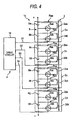
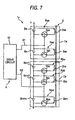
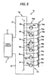
- the voltage equalizer 1x shown in Fig. 1 shows a case of division into two blocks Ca and Cb each including four loop circuits Raa... or Rba..., however, Fig. 4, Fig. 7 and Fig. 8 show examples in which the method of division of the blocks Ca... is modified.
- the modified example shown in Fig. 4 comprises a first block Ca including two loop circuits Raa and Rab, a second block Cb including two loop circuits Rba and Rbb, a third block Cc including two loop circuits Rca and Rcb, and a fourth block Cd .
- including two loop circuits Rda and Rdb that is, an example of division into four blocks Ca, Cb, Cc, and Cd each including two of the loop circuits Raa..., Rba..., Rca..., or Rda... is shown. Therefore, basically, the voltage equalizer 1x relating to the present invention can be divided into a plurality of blocks Ca... each including an arbitrary number of loop circuits Raa....
- the voltage equalizer 1x shown in Fig. 4 is set so that, when the terminal voltages of the capacitors Ba... of the first block Ca are defined as E n , the number of windings of the coils 2aa... is defined as N n , the ON time of the switching elements 3aa... is defined as T n , the terminal voltages of the capacitors Bc... of the second block Cb are defined as E n+1 , the number of windings of the coils 2ba... is defined as N n+1 , the ON time of the switching elements 3ba... is defined as T n+1 , the terminal voltages of the capacitors Be... of the third block Cc are defined as E n+2 , the number of windings of the coils 2ca...
- the ON time of the switching elements 3ca... is defined as T n+2
- the ON time of the switching elements 3ca... is defined as T n+2
- the terminal voltages of the capacitors Bg... of the fourth block Cd are defined as E n+3
- the number of windings of the coils 2da... is defined as N n+3
- the ON time of the switching elements 3da is defined as N n+2
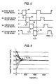
- pulse signals S1, S2, S3 and S4 of different timings as shown in Figs. 5 are supplied to the blocks Ca, Cb, Cc, and Cd, respectively, and the switching elements 3aa... of the respective blocks Ca... are collectively controlled to be ON by a block C... basis.
- the switching elements 3aa and 3ab of the first block Ca are controlled to be ON for only the time T n by the pulse signal S1, and then, the switching elements 3ba and 3bb of the second block Cb are controlled to be ON for only the time T n+1 by the pulse signal S2, and next, the switching elements 3ca and 3cb of the third block Cc are controlled to be ON for only the time T n+2 by the pulse signal S3, and thereafter, the switching elements 3da and 3db of the fourth block Cd are controlled to be ON for only the time T n+3 by the pulse signal S4. Thereafter, the operation to control the switching elements 3aa... of the first block Ca to be ON again for only the time T n by the pulse signal S1 is repeated in order.
- the coils 2ba, 2bb, 2da, and 2db are connected so that the winding directions thereof become reverse to those of the coils 2aa, 2ab, 2ca, and 2cb.
- Fig. 4 the same portions as in Fig. 1 are attached with the same symbols to make the construction clear, and detailed description of these is omitted.
- the modified example shown in Fig. 7 shows, in particular, a case where the number of the loop circuits Raa... in the first block Ca and the number of the loop circuits Rba... in the second block Cb are made different from each other although the point that the two blocks Ca and Cb are provided is the same as in the voltage equalizer 1x shown in Fig. 1. Even in such a case, basically, the same voltage equalizing operation as that of the voltage equalizer 1x is carried out.
- Fig. 6 shows the equalization characteristics when the number of loop circuits Raa... in the first block Ca is set to eight, and the number of loop circuits Rba... in the second block Cb is set to twelve.
- Fig. 6 shows the equalization characteristics when the number of loop circuits Raa... in the first block Ca is set to eight, and the number of loop circuits Rba... in the second block Cb is set to twelve.
- the modified example shown in Fig. 8 shows, in particular, a case where the plurality of capacitors Ba... at arbitrary connect positions are included in one of the blocks Ca... although the point where the two blocks Ca and Cb are provided is the same as in the voltage equalizer 1x shown in Fig. 1.
- the capacitors Ba... of each of the blocks Ca... are not necessarily continuously connected in series, and may be positioned at arbitrary connect positions.
- Fig. 8 shows an example in which, among the six capacitors Ba... connected in series, every other capacitor Ba, Bc, and Be are included in the first block Ca, and the remaining capacitors Bb, Bd, and Bf are included in the second block Cb.
- every other capacitor Ba, Bc, and Be are included in the first block Ca
- the remaining capacitors Bb, Bd, and Bf are included in the second block Cb.
- the symbols 3aa, 3ab, 3ac, 3ba, 3bb, and 3bc denote switching elements, respectively
- the symbols 2aa, 2ab, 2ac, 2ba, 2bb, and 2bc denote coils, respectively.
- the same portions as in Fig. 1 are attachedwith the same symbols to make the construction clear, and detailed description of these is omitted.
- the second embodiment shown in Fig. 9 shows a case where a part of the voltage equalizer 1x shown in Fig. 8 from which the drive circuit 10 is excluded is constructed as one module, and a plurality of modules M1 and M2 are combined to construct the voltage equalizer 1y.
- the voltage equalizer 1y comprises two modules M1 and M2 in which transformers 2 having a plurality of coils 2aa... corresponding to respective capacitors Ba... and a plurality of switching elements 3aa... corresponding to the respective coils 2aa... are provided, and the coils 2aa..., the switching 3aa..., and the capacitors Ba... are connected in series to each other to form a plurality of loop circuits Raa..., and the loop circuits Raa...
- the drive circuit 10 can be commonly used for the plurality of modules M1 M2..., and the number of the modules M1, M2... can be arbitrarily combined, and these are advantageous in terms of cost, adaptability, and versatility.
- Fig. 9 the same portions as in Fig. 8 (Fig. 1) are attached with the same symbols to make the construction clear, and detailed description of these is omitted.
- the control unit 4 which collectively controls the switching elements 3aa... of the respective blocks Ca... to be ON by a block Ca... basis by selectively supplying pulse signals S1.... of different timings to the plurality of divided blocks Ca..., and is set so that the polarities of the coils 2aa... of the blocks Ca... alternately reverse, so that problems which cause an increase in the size of the transformer 2 orrequire a separate measure to be taken for the one-directional magnetizing force of the transformer 2 can be eliminated. Furthermore, since the coils 2aa..., the switching elements 3aa..., and the capacitors Ba... are connected in series to form a plurality of loop circuits Raa..., cost reduction along with reduction in the number of parts and simplification and downsizing of the voltage equalizer are realized.
- the present invention is not limited to these examples, and arbitrary changes, additions, and omissions in the detailed circuitry and method, etc., without deviation from the spirit of the present invention are possible.
- the FETs 30 are illustrated as the switching elements 3aa..., they can be replaced with other switching elements having the same functions such as transistors.
- the capacitors Ba... are preferably used for a battery B to be loaded into an electric vehicle that runs by a motor or a hybrid vehicle that runs by using both engine andmotor, however, the use of the present invention is not limited to these.
- a transformer having a plurality of coils corresponding to capacitors and a plurality of switching elements corresponding to the coils are provided so that the coils, the switching elements, and the capacitors are connected in series to each other to form a plurality of loop circuits, the loop circuits is divided into a plurality of blocks each including an arbitrary number of loop circuits, and a control unit is also provided to collectively control the switching elements of the respective blocks to be ON by a block basis by selectively supplying pulse signals of different timings to the respective blocks, and make settings or controls so that the polarities of the coils of the respective blocks alternately reverse. Therefore, the voltage equalizer of the present invention has the following great effects.
Landscapes
- Engineering & Computer Science (AREA)
- Power Engineering (AREA)
- Charge And Discharge Circuits For Batteries Or The Like (AREA)
- Secondary Cells (AREA)
- Electric Propulsion And Braking For Vehicles (AREA)
- Dc-Dc Converters (AREA)
- Networks Using Active Elements (AREA)
Abstract
Description
Claims (10)
- A voltage equalizer for capacitors which equalizes terminal voltages of a plurality of capacitors connected in series, comprising:a transformer having a plurality of coils corresponding to the capacitors;a plurality of switching elements corresponding to the coils, wherein the coils, the switching elements, and the capacitors are connected in series to each other to form a plurality of loop circuits, the loop circuits are divided into a plurality of blocks each including an arbitrary number of loop circuits; anda control unit collectively controlling the switching elements of the respective blocks to be ON by a block basis by selectively supplying pulse signals of different timings to the respective blocks and makings settings or controls so that polarities of the coils of the blocks alternately reverse.
- The voltage equalizer for capacitors according to Claim 1, wherein the coils are connected so that the polarities of corresponding coils are in reverse to each other.
- The voltage equalizer for capacitors according to Claim 1, wherein in a case where terminal voltages of capacitors of a block having switching elements to be controlled to be ON n-th are defined as En, the number of windings of the corresponding coils is defined as Nn, an ON time of the switching element is defined as Tn, terminal voltages of the capacitors of a block having sswitching elements to be controlled to be ON n+1-th are defined as En+1, the number of windings of the corresponding coils is defined as Nn+1, and an ON time of the switching element is defined as Tn+1, a condition of En/En+1 = (Nn/Nn+1) · (Tn+1/Tn) is satisfied.
- The voltage equalizer for capacitors according to Claim 1, wherein the control unit monitors terminal voltages of the capacitors, and when scattering of the terminal voltages falls within a predetermined range, the control unit controls to stop ON-control of the switching elements or shortens an ON time.
- The voltage equalizer for capacitors according to Claim 1, wherein the control unit monitors currents flowing in the capacitors, and when currents equal to or more than a predetermined value flow in the capacitors, the control unit stops ON-control of the switching elements or shortens an ON time.
- The voltage equalizer for capacitors according to Claim 1, wherein each capacitor comprises one cell or a plurality of cells.
- The voltage equalizer for capacitors according to Claim 1, further comprising:wherein the capacitors of the respective modules are connected in series, and the transformers of the respective modules have equalizing coils respectively so that the equalizing coils are connected in parallel to each other.a plurality of modules each having a transformer with a plurality of coils corresponding to capacitors and a plurality of switching elements corresponding to the coils, wherein the coils, the switching elements, and the capacitors are connected in series to each other to form a plurality of loop circuits, the loop circuits are divided into a plurality of blocks each including an arbitrary number of loop circuits,
- The voltage equalizer for capacitors according to Claim 1, wherein the capacitors are used for a battery to be loaded into an electric vehicle which runs by a motor or a hybrid vehicle which runs by using both engine and motor.
- The voltage equalizer for capacitors according to Claim 6, wherein the capacitors are used for a battery to be loaded into an electric vehicle which runs by a motor or a hybrid vehicle which runs by using both engine and motor.
- The voltage equalizer for capacitors according to Claim 7, wherein the capacitors are used for a battery to be loaded into an electric vehicle which runs by a motor or a hybrid vehicle which runs by using both engine and motor.
Applications Claiming Priority (2)
| Application Number | Priority Date | Filing Date | Title |
|---|---|---|---|
| JP2003118657 | 2003-04-23 | ||
| JP2003118657A JP3848635B2 (en) | 2003-04-23 | 2003-04-23 | Voltage equalization device for storage element |
Publications (2)
| Publication Number | Publication Date |
|---|---|
| EP1471618A2 true EP1471618A2 (en) | 2004-10-27 |
| EP1471618A3 EP1471618A3 (en) | 2005-06-08 |
Family
ID=32959633
Family Applications (1)
| Application Number | Title | Priority Date | Filing Date |
|---|---|---|---|
| EP04009698A Withdrawn EP1471618A3 (en) | 2003-04-23 | 2004-04-23 | Voltage equalizer for capacitors |
Country Status (3)
| Country | Link |
|---|---|
| US (1) | US20040212352A1 (en) |
| EP (1) | EP1471618A3 (en) |
| JP (1) | JP3848635B2 (en) |
Families Citing this family (19)
| Publication number | Priority date | Publication date | Assignee | Title |
|---|---|---|---|---|
| US7560904B2 (en) * | 2005-10-03 | 2009-07-14 | Lear Corporation | Method and system of managing power distribution in switch based circuits |
| JP4621635B2 (en) * | 2006-07-05 | 2011-01-26 | Fdk株式会社 | Series cell voltage balance correction circuit |
| US9397508B2 (en) | 2009-05-22 | 2016-07-19 | Intersil Americas LLC | System and method for cell balancing and charging using a serially coupled inductor and capacitor |
| US8541980B2 (en) * | 2009-05-22 | 2013-09-24 | Intersil Americas LLC | System and method for cell balancing and charging |
| CN102035010B (en) * | 2009-09-29 | 2013-05-01 | 凹凸电子(武汉)有限公司 | Battery unit equalizing circuit and method |
| DE102010008010A1 (en) * | 2010-02-15 | 2011-08-18 | Li-Tec Battery GmbH, 01917 | circuitry |
| JP2011188789A (en) * | 2010-03-15 | 2011-09-29 | Yanmar Co Ltd | Electric riding mower |
| EP2805598A1 (en) | 2010-03-01 | 2014-11-26 | Yanmar Co., Ltd. | Electric riding mower |
| US8773071B2 (en) * | 2010-11-01 | 2014-07-08 | The Boeing Company | System and method for cell voltage balancing |
| CA2822593A1 (en) | 2010-12-22 | 2012-06-28 | Ge Energy Power Conversion Technology Limited | Mechanical arrangement of a multilevel power converter circuit |
| MX2013007362A (en) | 2010-12-22 | 2013-12-16 | Ge Energy Power Conversion Technology Ltd | CAPACITOR COMPENSATOR CIRCUIT AND CONTROL METHOD FOR AN ELECTRONIC DEVICE SUCH AS A MULTIPLE LEVEL POWER INVERTER. |
| JP2012239300A (en) * | 2011-05-11 | 2012-12-06 | Shindengen Electric Mfg Co Ltd | Cell balance circuit and cell balance device |
| JP5980031B2 (en) * | 2012-07-23 | 2016-08-31 | 南通江海電容器股▲分▼有限公司 | Charge transfer circuit of power storage device in which power storage elements are connected in series |
| JP6146321B2 (en) * | 2014-01-20 | 2017-06-14 | 株式会社デンソー | Power supply |
| KR101567423B1 (en) * | 2014-06-24 | 2015-11-09 | (주) 세스 | Active balancing controller of baterry management system for electronic storage system utilizing small multi winding transformer |
| DE102017202204A1 (en) * | 2017-02-13 | 2018-08-16 | Siemens Aktiengesellschaft | Converter arrangement |
| CN106787021B (en) * | 2017-03-16 | 2023-11-17 | 山东大学 | A modular system and method for battery pack equalizer based on multi-winding transformer |
| DE102019208207A1 (en) * | 2019-06-05 | 2020-12-10 | Siemens Aktiengesellschaft | DC / DC converter for converting a direct voltage in the medium voltage range into a direct voltage in the low voltage range |
| CN115020080B (en) * | 2022-07-01 | 2026-04-24 | 深圳市猿芯半导体有限责任公司 | A winding structure for a multi-channel integrated synchronous coil |
Family Cites Families (2)
| Publication number | Priority date | Publication date | Assignee | Title |
|---|---|---|---|---|
| DE4422409C2 (en) * | 1994-06-29 | 1996-07-11 | Fraunhofer Ges Forschung | Device for the exchange of charges between a plurality of energy stores or converters connected in series |
| US6642693B2 (en) * | 2000-11-21 | 2003-11-04 | Nagano Japan Radio Co., Ltd. | Voltage equalizing apparatus for battery devices |
-
2003
- 2003-04-23 JP JP2003118657A patent/JP3848635B2/en not_active Expired - Fee Related
-
2004
- 2004-04-23 US US10/830,879 patent/US20040212352A1/en not_active Abandoned
- 2004-04-23 EP EP04009698A patent/EP1471618A3/en not_active Withdrawn
Also Published As
| Publication number | Publication date |
|---|---|
| JP3848635B2 (en) | 2006-11-22 |
| US20040212352A1 (en) | 2004-10-28 |
| EP1471618A3 (en) | 2005-06-08 |
| JP2004328868A (en) | 2004-11-18 |
Similar Documents
| Publication | Publication Date | Title |
|---|---|---|
| US20040212352A1 (en) | Voltage equalizer for capacitors | |
| US7939965B2 (en) | Charge of equalization apparatus with parallel connection of secondary windings of multiple transformers | |
| JP5502918B2 (en) | Charge / discharge device for battery pack | |
| JP6173922B2 (en) | Battery for managing cells individually | |
| US8810199B2 (en) | Charge equalization between series-connected battery cells | |
| US7804276B2 (en) | Circuit arrangement and method for transferring electrical charge between accumulators of an accumulator arrangement including a series circuit of accumulators | |
| US6642693B2 (en) | Voltage equalizing apparatus for battery devices | |
| US20200169097A1 (en) | Modularization system and method for battery equalizers based on multi- winding transformers | |
| JP6019519B2 (en) | Battery cell balancing converter | |
| CN101849340A (en) | Battery management system integrated with voltage sensor and charge equalizer | |
| US20120249058A1 (en) | Auxiliary battery charging apparatus | |
| JP2013219994A (en) | Battery equalization device and method | |
| KR20120112072A (en) | Auxiliary battery charging apparatus | |
| WO2013114757A1 (en) | Battery equalization device and method | |
| CN106558995A (en) | DC/DC conversion equipments | |
| JP2004236486A (en) | Battery voltage detector | |
| US20120212056A1 (en) | Modularized balancing bridge for multiple voltage sources | |
| CN117578882A (en) | Control circuit and method for single-mode dual current path buck-boost converter | |
| RU37884U1 (en) | BATTERY VOLTAGE LEVELING DEVICE | |
| JP2004201361A (en) | Storage device voltage equalization device | |
| JP2005017156A (en) | Battery abnormality detection device | |
| JP7496189B1 (en) | Battery-powered DC power supply | |
| Yang et al. | A High-Frequency AC-Linked Active Multicell Balancing Topology for Series-Connected Batteries | |
| KR20260029142A (en) | Electrified vehicle | |
| KR20260029143A (en) | Electrified vehicle |
Legal Events
| Date | Code | Title | Description |
|---|---|---|---|
| PUAI | Public reference made under article 153(3) epc to a published international application that has entered the european phase |
Free format text: ORIGINAL CODE: 0009012 |
|
| AK | Designated contracting states |
Kind code of ref document: A2 Designated state(s): AT BE BG CH CY CZ DE DK EE ES FI FR GB GR HU IE IT LI LU MC NL PL PT RO SE SI SK TR |
|
| AX | Request for extension of the european patent |
Extension state: AL HR LT LV MK |
|
| PUAL | Search report despatched |
Free format text: ORIGINAL CODE: 0009013 |
|
| AK | Designated contracting states |
Kind code of ref document: A3 Designated state(s): AT BE BG CH CY CZ DE DK EE ES FI FR GB GR HU IE IT LI LU MC NL PL PT RO SE SI SK TR |
|
| AX | Request for extension of the european patent |
Extension state: AL HR LT LV MK |
|
| 17P | Request for examination filed |
Effective date: 20050803 |
|
| AKX | Designation fees paid |
Designated state(s): DE FR |
|
| RAP1 | Party data changed (applicant data changed or rights of an application transferred) |
Owner name: FUJI JUKOGYO KABUSHIKI KAISHA Owner name: NAGANO JAPAN RADIO CO., LTD. |
|
| STAA | Information on the status of an ep patent application or granted ep patent |
Free format text: STATUS: THE APPLICATION IS DEEMED TO BE WITHDRAWN |
|
| 18D | Application deemed to be withdrawn |
Effective date: 20141101 |