EP1471588A1 - Semiconductor device having fuel cell and its manufacturing method - Google Patents
Semiconductor device having fuel cell and its manufacturing method Download PDFInfo
- Publication number
- EP1471588A1 EP1471588A1 EP03703040A EP03703040A EP1471588A1 EP 1471588 A1 EP1471588 A1 EP 1471588A1 EP 03703040 A EP03703040 A EP 03703040A EP 03703040 A EP03703040 A EP 03703040A EP 1471588 A1 EP1471588 A1 EP 1471588A1
- Authority
- EP
- European Patent Office
- Prior art keywords
- separator
- semiconductor
- semiconductor device
- fuel cell
- semiconductor element
- Prior art date
- Legal status (The legal status is an assumption and is not a legal conclusion. Google has not performed a legal analysis and makes no representation as to the accuracy of the status listed.)
- Granted
Links
Images





Classifications
-
- H—ELECTRICITY
- H10—SEMICONDUCTOR DEVICES; ELECTRIC SOLID-STATE DEVICES NOT OTHERWISE PROVIDED FOR
- H10W—GENERIC PACKAGES, INTERCONNECTIONS, CONNECTORS OR OTHER CONSTRUCTIONAL DETAILS OF DEVICES COVERED BY CLASS H10
- H10W42/00—Arrangements for protection of devices
-
- H—ELECTRICITY
- H01—ELECTRIC ELEMENTS
- H01M—PROCESSES OR MEANS, e.g. BATTERIES, FOR THE DIRECT CONVERSION OF CHEMICAL ENERGY INTO ELECTRICAL ENERGY
- H01M4/00—Electrodes
- H01M4/86—Inert electrodes with catalytic activity, e.g. for fuel cells
- H01M4/8605—Porous electrodes
-
- H—ELECTRICITY
- H01—ELECTRIC ELEMENTS
- H01M—PROCESSES OR MEANS, e.g. BATTERIES, FOR THE DIRECT CONVERSION OF CHEMICAL ENERGY INTO ELECTRICAL ENERGY
- H01M8/00—Fuel cells; Manufacture thereof
- H01M8/02—Details
-
- H—ELECTRICITY
- H01—ELECTRIC ELEMENTS
- H01M—PROCESSES OR MEANS, e.g. BATTERIES, FOR THE DIRECT CONVERSION OF CHEMICAL ENERGY INTO ELECTRICAL ENERGY
- H01M8/00—Fuel cells; Manufacture thereof
- H01M8/02—Details
- H01M8/0202—Collectors; Separators, e.g. bipolar separators; Interconnectors
- H01M8/0258—Collectors; Separators, e.g. bipolar separators; Interconnectors characterised by the configuration of channels, e.g. by the flow field of the reactant or coolant
-
- H—ELECTRICITY
- H01—ELECTRIC ELEMENTS
- H01M—PROCESSES OR MEANS, e.g. BATTERIES, FOR THE DIRECT CONVERSION OF CHEMICAL ENERGY INTO ELECTRICAL ENERGY
- H01M8/00—Fuel cells; Manufacture thereof
- H01M8/10—Fuel cells with solid electrolytes
- H01M8/1007—Fuel cells with solid electrolytes with both reactants being gaseous or vaporised
-
- H—ELECTRICITY
- H01—ELECTRIC ELEMENTS
- H01M—PROCESSES OR MEANS, e.g. BATTERIES, FOR THE DIRECT CONVERSION OF CHEMICAL ENERGY INTO ELECTRICAL ENERGY
- H01M8/00—Fuel cells; Manufacture thereof
- H01M8/24—Grouping of fuel cells, e.g. stacking of fuel cells
- H01M8/241—Grouping of fuel cells, e.g. stacking of fuel cells with solid or matrix-supported electrolytes
-
- H—ELECTRICITY
- H10—SEMICONDUCTOR DEVICES; ELECTRIC SOLID-STATE DEVICES NOT OTHERWISE PROVIDED FOR
- H10D—INORGANIC ELECTRIC SEMICONDUCTOR DEVICES
- H10D88/00—Three-dimensional [3D] integrated devices
-
- Y—GENERAL TAGGING OF NEW TECHNOLOGICAL DEVELOPMENTS; GENERAL TAGGING OF CROSS-SECTIONAL TECHNOLOGIES SPANNING OVER SEVERAL SECTIONS OF THE IPC; TECHNICAL SUBJECTS COVERED BY FORMER USPC CROSS-REFERENCE ART COLLECTIONS [XRACs] AND DIGESTS
- Y02—TECHNOLOGIES OR APPLICATIONS FOR MITIGATION OR ADAPTATION AGAINST CLIMATE CHANGE
- Y02E—REDUCTION OF GREENHOUSE GAS [GHG] EMISSIONS, RELATED TO ENERGY GENERATION, TRANSMISSION OR DISTRIBUTION
- Y02E60/00—Enabling technologies; Technologies with a potential or indirect contribution to GHG emissions mitigation
- Y02E60/30—Hydrogen technology
- Y02E60/50—Fuel cells
-
- Y—GENERAL TAGGING OF NEW TECHNOLOGICAL DEVELOPMENTS; GENERAL TAGGING OF CROSS-SECTIONAL TECHNOLOGIES SPANNING OVER SEVERAL SECTIONS OF THE IPC; TECHNICAL SUBJECTS COVERED BY FORMER USPC CROSS-REFERENCE ART COLLECTIONS [XRACs] AND DIGESTS
- Y02—TECHNOLOGIES OR APPLICATIONS FOR MITIGATION OR ADAPTATION AGAINST CLIMATE CHANGE
- Y02P—CLIMATE CHANGE MITIGATION TECHNOLOGIES IN THE PRODUCTION OR PROCESSING OF GOODS
- Y02P70/00—Climate change mitigation technologies in the production process for final industrial or consumer products
- Y02P70/50—Manufacturing or production processes characterised by the final manufactured product
Definitions
- the present invention relates to a semiconductor device equipped with a fuel cell, and a method for producing the same.
- Such a semiconductor device per se can be equipped with a power source (i.e., it is a semiconductor device equipped with a power source), further superiority in versatility is provided to the semiconductor device.
- a generally used secondary battery such as a lithium battery may be used as a power source.
- a power source having a considerably large size as compared with that of a semiconductor element is required due to output characteristics of the secondary battery. Therefore, the miniaturization of a semiconductor device equipped with a power source has a limit.
- a battery since a battery has to be charged or replaced when the battery is exhausted, there is a problem in versatility.
- the recycling of secondary batteries is expected to become a significant social issue in the future. Considering these situations, further compact and versatile semiconductor devices equipped with power sources are sought.
- a semiconductor device equipped with a fuel cell includes a fuel cell and a semiconductor element, and the fuel cell includes an anode separator in which a flow channel for fuel is formed, a cathode separator in which a flow channel for oxidizer is formed, and a membrane electrode assembly interposed between the anode separator and the cathode separator.
- the semiconductor element is formed on one of principal surfaces of one separator selected from the anode separator and the cathode separator, and the semiconductor element and the selected separator are connected electrically.
- the foregoing semiconductor device may include two of the semiconductor elements, which are a first semiconductor element formed on one of the principal surfaces of the anode separator, and a second semiconductor element formed on one of the principal surfaces of the cathode separator.
- the selected separator may be formed with a semiconductor substrate.
- the semiconductor substrate may be made of crystalline silicon.
- the semiconductor substrate may be made of a compound semiconductor containing an element of the group IIIb and an element of the group Vb.
- the semiconductor substrate may be made of a compound semiconductor containing an element of the group IIb and an element of the group VIb.
- the anode separator may be formed with a N-type semiconductor substrate and the cathode separator with a P-type semiconductor substrate.
- the fuel cell further may include a contact layer arranged between the selected separator and the membrane electrode assembly so as to reduce a contact resistance between the selected separator and the membrane electrode assembly.
- the fuel cell may further include an insulation layer formed between the semiconductor element and the selected separator.
- the semiconductor element is connected electrically with the selected separator via an electrode formed in the insulation layer.
- the insulation layer may be made of SiO 2 .
- the insulation layer has a specific resistance of not less than 10 5 ⁇ cm.
- the insulation layer may have a thickness in a range of 10 nm to 1 ⁇ m.
- the selected separator may be made of a metal.
- the insulation layer may be a metal oxide film.
- the foregoing semiconductor device may be configured so that the semiconductor element includes a first electrode and a second electrode, the first electrode is connected electrically with the anode separator, and the second electrode is connected electrically with the cathode separator.
- the foregoing semiconductor device may be configured so that the semiconductor element is a N-channel MOS transistor, a source electrode and a substrate electrode of the N-channel MOS transistor are connected electrically with the anode separator, and a drain electrode and a gate electrode of the N-channel MOS transistor are connected electrically with the cathode separator.
- the foregoing semiconductor device may be configured so that the semiconductor element is a P-channel MOS transistor, a source electrode and a gate electrode of the P-channel MOS transistor are connected electrically with the anode separator, and a drain electrode and a substrate electrode of the P-channel MOS transistor are connected electrically with the cathode separator.
- the fuel cell may be formed by stacking a plurality of cells, each of which includes the anode separator, the cathode separator, and the membrane electrode assembly.
- a method of the present invention for producing a semiconductor device equipped with a fuel cell is a method for producing a semiconductor device equipped with a fuel cell having a structure in which a membrane electrode assembly is interposed between a pair of separators.
- the method includes the steps of: (i) forming a semiconductor element on one surface of a semiconductor substrate; (ii) forming a flow channel through which either fuel or oxidizer is to flow on a surface of the semiconductor substrate that is opposite to the surface on which the semiconductor element is formed; and (iii) laminating the membrane electrode assembly on the semiconductor substrate so that the surface of the semiconductor substrate with the flow channel thereon is in contact with the membrane electrode assembly, wherein the semiconductor substrate serves as one separator selected from the pair of separators.
- the semiconductor substrate may include an insulation layer between the surface with the semiconductor element thereon and the surface with the flow channel thereon.
- the step (i) may include a sub-step of: (a) forming the semiconductor element on the insulation layer in a manner such that the semiconductor element and the semiconductor substrate are connected electrically with each other via an electrode formed in the insulation layer.
- Another method of the present invention for producing a semiconductor device equipped with a fuel cell is a method for producing a semiconductor device equipped with a fuel cell having a structure in which a membrane electrode assembly is interposed between a pair of separators.
- the method includes the steps of: (I) forming a flow channel through which either fuel or oxidizer is to flow on a surface of the semiconductor substrate; (II) forming a semiconductor element on a surface of the semiconductor substrate that is opposite to the surface on which the flow channel is formed; and (III) laminating the membrane electrode assembly on the semiconductor substrate so that the surface of the semiconductor substrate with the flow channel thereon is in contact with the membrane electrode assembly, wherein the semiconductor substrate serves as one separator selected from the pair of separators.
- the semiconductor substrate may include an insulation layer between the surface with the flow channel thereon and the surface with the semiconductor element thereon.
- the step (II) may include a sub-step of (A) forming the semiconductor element on the insulation layer in a manner such that the semiconductor element and the semiconductor substrate are connected electrically with each other via an electrode formed in the insulation layer.
- FIG. 1 is a cross-sectional view illustrating an example of a semiconductor device equipped with a fuel cell (hereinafter sometimes referred to as semiconductor device) according to the present invention.
- the semiconductor device shown in FIG. 1 is equipped with a fuel cell 1 and a semiconductor element 2.
- the fuel cell 1 includes an anode separator 12 in which flow channels 11 for fuel are formed, a cathode separator 14 in which flow channels 13 for oxidizer are formed, and a membrane electrode assembly (MEA) 15 that is interposed between the anode separator 12 and the cathode separator 14.
- the semiconductor element 2 is formed on one of the principal surfaces of one separator selected from the anode separator 12 and the cathode separator 14 (in the example shown in FIG. 1, on one principal surface of the anode separator 12) so that the semiconductor element 2 and the one separator (i.e., the anode separator 12 in the example of FIG. 1) are connected electrically with each other.
- the fuel cell and the semiconductor element are provided integrally, and the fuel cell as a power source has the following characteristics: it has a high energy density (for instance, it can be increased by one or more orders as compared with a lithium secondary battery as a typical secondary battery); it does not require charging, replacement, or the like as is the case with the battery when it is exhausted; and it starts electric power generation immediately when fuel is supplied. Therefore, this configuration can provide the semiconductor device having excellent compactness and versatility. Further, since it basically generates electrical power as long as fuel is supplied, the problem of recycling can be minimized as compared with the secondary battery.
- the semiconductor element 2 is formed on an insulation layer 3 arranged on one principal surface of the anode separator 12 as the aforementioned one separator (in other words, an insulation layer 3 is formed between the semiconductor element 2 and the foregoing one separator), and the semiconductor element 2 and the foregoing one separator are connected electrically via an electrode 4 formed in the insulation layer 3.
- this semiconductor device can configure a so-called SOI (silicon on insulator) transistor, which is capable of operating at a high speed even with a power supply voltage in a low-voltage range of not more than 1 V.
- SOI silicon on insulator
- Such a SOI transistor which has been commercialized for practical use in a wristwatch or the like, can be actuated even if a fuel cell 1 is a single cell, since it can operate with a voltage of not more than 1 V.
- this also makes it possible to reduce the power consumption of the semiconductor element 2, this causes a circuit to operate for a longer period. Therefore, this can provide the semiconductor device having further excellent compactness and versatility. Furthermore, since the insulation layer generally has a low thermal conductivity, heat generated by the fuel cell 1 can be prevented from being transmitted to the semiconductor element 2.
- the fuel cell 1 includes a configuration in which the MEA 15 is interposed between the anode separator 12 and the cathode separator 14.
- the flow channels 11 for fuel are formed in the anode separator 12, while the flow channels 13 for oxidizer are formed in the cathode separator 14.
- the MEA 15 may be at least in contact with surfaces of the respective separators where the foregoing flow channels are formed. With the supply of the fuel and the oxidizer to the MEA 15 through the flow channels 11 and 13, the electric power generation is carried out. Further, the anode separator 12 and the cathode separator 14 also function as charge collectors for collecting the electric power generated in the MEA 15.
- the structure, material, size, and shape of the MEA 15 are not limited particularly, as long as the MEA 15 is capable of generating electric power with supply of a fuel and an oxidizer. They may be set appropriately according to types of a fuel and an oxidizer for use in the electric power generation, a temperature range in which the electric power generation is carried out, required characteristics of the electric power generation, etc.
- An example of the structure of the MEA 15 is, for instance, such that anode electrodes 152 and cathode electrodes 153 are applied or printed on opposed surfaces of a film 151 made of a polyelectrolyte. Further, a certain layer such as a diffusion layer may be provided additionally in the MEA as required.
- the fuel cell 1 is a so-called PEFC (polyelectrolyte fuel cell), which is capable of generating electric power in a relatively low temperature range (for instance, in a range of 0°C to 100°C).
- PEFC polyelectrolyte fuel cell
- the electric power generation temperature By setting the electric power generation temperature to, for instance, not higher than 80°C, the influence of heat on the semiconductor element 2 can be minimized. Further, since the PEFC has a particularly high energy density among fuel cells, it is capable of obtaining necessary electric power even if it is of a small size. Therefore, this can provide the semiconductor device having further excellent compactness and versatility.
- the fuel and oxidizer supplied to the fuel cell 1 are not limited particularly, as long as they allow the fuel cell 1 to generate electric power. They may be selected appropriately according to the temperature range in which the electric power generation is carried out, required characteristics of the electric power generation, etc.
- As the oxidizer air, for instance, may be used.
- the fuel include not only a gas such as hydrogen but also a liquid such as methanol.
- the fuel cell 1 is a DMFC (direct methanol fuel cell) as one type of the PEFC. In this case, as compared with the case where a gas such as hydrogen is used as the fuel, the supply of the fuel is carried out more easily.
- a method for supplying the fuel and oxidizer to the fuel cell 1 is not limited particularly. For instance, they may be supplied to the corresponding flow channels of the separators using devices such as pumps. In the case where air is used as the oxidizer, the flow channels in the cathode separator may be opened to the atmosphere. An example wherein the foregoing flow channels are opened to the atmosphere will be described in the third embodiment.
- a material used for forming the anode separator 12 is not limited particularly, as long as the anode separator 12 thus formed functions as a charge collector (in other words, as long as the anode separator 13 thus formed has a conductivity of not lower than a certain level), and allows the insulation layer 3 to be formed on one of principal surfaces of the anode separator 12.
- the use of a material having a specific resistance of, for instance, not more than 100 ⁇ ⁇ cm is recommendable so as to allow the anode separator 12 to function as a charge collector.
- the anode separator 12 may be formed using a substrate made of carbon such as graphite, a substrate made of a metal such as stainless steel, or a semiconductor substrate.
- a material used for forming the cathode separator 14 is not limited particularly, as long as the cathode separator 14 thus formed functions as a charge collector (in other words, as described above, as long as the cathode separator 14 formed has a conductivity of not lower than a certain level). More specifically, for instance, the cathode separator 14 may be formed using a substrate made of carbon such as graphite, a substrate made of a metal such as stainless steel, or a semiconductor substrate. It should be noted that the material used for forming the anode separator 12 and the material used for forming the cathode separator 14 may be the same, or may be different.
- a semiconductor substrate made of crystalline silicon may be used for forming a separator, irrespective of whether it is the anode separator 12 or the cathode separator 14.
- the separator obtained sometimes does not have a sufficient conductivity as a charge collector.
- the semiconductor substrate may be doped with an impurity such as an element of the group IIb, the group IIIb, the group Vb, the group VIb, or the like, so as to have an increased conductivity.
- an impurity may be doped in an entirety of the semiconductor substrate, or alternatively, only in a part that requires the doping.
- the semiconductor substrate has either N-type or P-type conductivity, depending on the type of the impurity.
- a semiconductor substrate of any type of conductivity, the P-type or the N-type may be used.
- the conductivity of the anode separator and that of the cathode separator may be the same type, or may be different types.
- the anode separator 12 is formed with a N-type semiconductor substrate and the cathode separator 14 is formed with a P-type semiconductor substrate.
- the flow of electrons from the anode to the cathode can be made smoother, whereby the characteristics of the fuel cell 1 can be enhanced further. Therefore, this can make the semiconductor device more excellent in versatility.
- examples of the semiconductor substrate used herein include substrates composed of compound semiconductors containing elements of the group IIIb and the group Vb, such as GaN, GaP, GaAs, etc. Further, examples of the semiconductor substrate used herein also include substrates composed of compound semiconductors containing elements of the group IIb and the group VIb, such as ZnS, ZnSe, etc.
- the use of the semiconductor substrate for forming the separator allows the semiconductor processing process to be applied therein, thereby allowing the flow channels and the like to be formed by micromachining. For instance, it is possible to form a thin fuel cell with an overall thickness of less than 1.5 mm. Further, the semiconductor substrate is chemically stable, and in a PEFC, the corrosion of the separator can be suppressed to a minimum level, even in the flow channels therein that are considered to be in a strongly acid atmosphere. Further, since the fuel does not pass through the semiconductor substrate, even in the case where a minute separator is formed, a leakage of the fuel through the separator can be suppressed to a minimum level. Furthermore, since the already available semiconductor processing process is applicable for the production, the separator can be formed integrally with the semiconductor element, whereby the semiconductor device can be produced with improved productivity.
- crystalline silicon has various advantages such as the abundance in the earth of silicon as its raw material, the harmlessness to human bodies, and the inexpensiveness. Moreover, a semiconductor substrate made of crystalline silicon is superior in the uniformness of the thickness and the flatness of the surfaces, and therefore the combination of the crystalline silicon substrate and the silicon micromachining technology enables processing with significant accuracy. Further, in the case where a large-diameter silicon wafer is subjected to a batch processing in a semiconductor processing line, a number of separators on the same wafer can be formed simultaneously. This enables low-cost production of separators.
- some crystalline silicon substrates available in the market have a specific resistance of, for instance, not more than about 10 m ⁇ cm.
- the separator with a thickness of, for instance, 650 ⁇ m has a resistance per unit area of approximately 0.65 m ⁇ /cm 2 (without taking contact resistance into consideration). This proves that the separator formed with a crystalline silicon substrate is capable of sufficiently functioning as a charge collector of a fuel cell.
- the resistance overvoltage of the separator is approximately 65 ⁇ V, which is considered to be sufficiently small as compared with an output voltage of a fuel cell (for instance, an open-circuit voltage (OCV) is approximately 1.1 V in the case where hydrogen is used as fuel).
- OCV open-circuit voltage
- a thickness of the anode separator 12 and that of the cathode separator 14 are not limited particularly, as long as the flow channels for the fuel and the oxidizer can be formed.
- the thickness is, for example, in a range of 10 ⁇ m to 1 mm. More specifically, in the case where a common 6-inch silicon substrate is used for forming a separator, for example, the thickness of the separator is approximately 650 ⁇ m.
- a size and a shape of the flow channels for the fuel and the oxidizer, and a percentage of the flow channels in an area of the separator are not limited particularly, as long as the fuel and the oxidizer can be supplied to the MEA. They may be set appropriately according to the thickness of the separator itself, required electric power generation characteristics, etc. For instance, in the example shown in FIG. 1, thirteen flow channels are formed in one separator, but the number of the flow channels may be set freely.
- the flow channels may be formed with a single flow channel in a bent form.
- each of the flow channels may be formed, for instance, in a rectangular shape with a width in a range of 10 ⁇ m to 200 ⁇ m, a depth in a range of 10 ⁇ m to 500 ⁇ m, and a space between adjacent flow channels (pitch) in a range of 10 ⁇ m to 100 ⁇ m.
- the semiconductor device of the present invention is not limited to this configuration particularly.
- the flow channels of the respective separators may face each other so that respective directions thereof form a certain relative angle.
- the separators may be formed and arranged so that the respective directions of the flow channels thereof cross perpendicularly.
- the semiconductor device shown in FIG. 1 may include a contact layer 16 for reducing contact resistance between the anode separator 12 as the foregoing one separator and the MEA 15 so that the contact layer 16 is interposed between the anode separator 12 and the MEA 15.
- the contact layer may be arranged between the cathode separator 14 and the MEA 15.
- the contact layer has a thickness, for instance, in a range of 0.01 ⁇ m to 10 ⁇ m, preferably in a range of 0.01 ⁇ m to 0.5 ⁇ m. Further, the contact layer is not necessarily arranged over an entirety of a surface of the separator, and a region where the contact layer is arranged may be determined appropriately.
- the contact layer 16 is not limited particularly, as long as the contact resistance between the separator and the MEA is reduced.
- a degenerated impurity-diffused layer having the same conductivity as the foregoing semiconductor substrate may be formed on the semiconductor substrate so as to serve as the contact layer.
- An example of a method for forming the impurity-diffused layer is such that ions of phosphor (P), arsenic (As), boron (B), or the like as an impurity are implanted at a dose of not less than 10 14 /cm 2 in a semiconductor substrate such as a crystalline silicon substrate, and are diffused therein.
- a metal silicide layer may be laminated over the impurity-diffused layer so that a laminated film of the impurity-diffused layer and the metal silicide layer serves as the contact layer. Furthermore, the foregoing laminate may further include another layer as required.
- the metal silicide layer may be made of, for instance, platinum silicide, cobalt silicide, molybdenum silicide, nickel silicide, or the like. A specific example of forming such a contact layer will be described later in the sixth embodiment.
- a material used for forming the insulation layer 3 is not limited particularly, as long as it is formed between the semiconductor element 2 and the anode separator 12.
- SiO 2 , glass, a metal oxide film, or the like may be used as the material.
- the material used may have a specific resistance in a range of, for instance, not less than 10 5 ⁇ cm.
- the insulation layer 3 may be formed by causing the foregoing material to adhere to the anode separator.
- the insulation layer 3 may be an insulation layer made of SiO 2 , for instance.
- SOI silicon on insulator
- the insulation layer 3 may be formed with a film of an oxide of the same metal.
- the insulation layer 3 can be formed by oxidizing a surface of the substrate made of the metal, and therefore, this can make the semiconductor device more excellent in stability and versatility. Further, this also makes it possible to produce the semiconductor device with improved productivity. Further, since the separator itself is made of a metal, the separator is caused to have a significantly small specific resistance in the ⁇ ⁇ cm order, and therefore, this further can reduce the resistance overvoltage of the fuel cell.
- the insulation layer 3 can be formed by oxidizing a surface of the anode separator 12. Therefore, this makes it possible to produce the semiconductor device with further improved productivity.
- the thickness of the insulation layer 3 is not limited particularly, as long as the insulation between the anode separator 12 and the semiconductor element 2 can be secured. For instance, it may be not less than 10 nm. In the case where the anode separator 12 is formed with a semiconductor substrate made of crystalline silicon and the insulation layer 3 is made of SiO 2 , the insulation layer 3 has a thickness in a range of, for instance, 10 nm to 1 ⁇ m. It should be noted that since the insulation layer 3 generally has a small thermal conductivity, an increase in the thickness of the insulation layer 3 can suppress the transmission of heat from the fuel cell 1 to the semiconductor element 2.
- the insulation layer 3 has a via hole in which the electrode 4 is formed (the electrode 4 electrically connects the semiconductor element 2 with the anode separator 12).
- the size of the via hole may be set according to the electrode 4, and is not limited particularly. For instance, it may have a cross-sectional area of not more than 1 ⁇ m 2 . Still further, though the insulation layer 3 shown in FIG. 1 has only a single via hole, the number of the via holes is not limited particularly. A plurality of the via holes may be provided as required.
- tungsten, aluminum, copper, or the like may be used.
- the electrode 4 may be provided integrally with element wiring 63 of the semiconductor element 2.
- CMOS inverter composed of an N-channel MOS transistor 21 and a P-channel MOS transistor 22 is formed, as the semiconductor element 2, on a crystalline silicon layer 51.
- the CMOS inverter is a common CMOS inverter that includes a P-well contact layer 52, a N-well contact layer 53, a P-type source electrode 54, a P-type drain electrode 55, a N-type drain electrode 56, a N-type source electrode 57, gate insulation films 58, a N-type gate electrode 59, a P-type gate electrode 60, an element separation insulation film 61, interlayer insulation films 62, element wiring 63, a P-well 64, and a N-well 65.
- Materials used in the foregoing respective regions, thicknesses and sizes of the foregoing regions are not limited particularly. For instance, they may be identical to those of a common semiconductor element.
- the CMOS inverter as a semiconductor element is formed on the crystalline silicon layer 51.
- the insulation layer 3 is made of SiO 2
- the anode separator 12 the insulation layer 3, and the semiconductor element 2 can be formed by processing a SOI substrate available in the market, and this can make the semiconductor device more excellent in stability and versatility. Further, this makes it possible to produce the semiconductor device with improved productivity.
- the thickness of the crystalline silicon layer 51 is not limited particularly. For instance, it is in a range of 0.01 ⁇ m to 10 ⁇ m.
- the crystalline silicon layer 51 has a specific resistance in a range of, for instance, 1 m ⁇ cm to 1 k ⁇ cm.
- the semiconductor element in the semiconductor device of the present invention may be configured so as to include first and second electrodes, the first electrode being connected electrically with the anode separator and the second electrode being connected electrically with the cathode separator.
- a ground potential electrode (V SS shown in FIG. 1) of the CMOS inverter as the semiconductor element is connected electrically with the anode separator 12 via the electrode 4 formed in the insulation layer 3. Electrons are supplied via this route to a load circuit of the CMOS inverter.
- a power supply electrode (V DD shown in FIG. 1) of the CMOS inverter is connected electrically with the cathode separator 14 via external wiring 66.
- CMOS inverter This allows electric current from the fuel cell 1 to flow into the power supply electrode of the CMOS inverter via the external wiring 66.
- input and output electrodes of the CMOS inverter are denoted as V in and V out in FIG. 1. Further, the electrode 4 and the ground potential electrode Vss may be provided integrally.
- the aforementioned contact layer or metal thin film layer may be arranged between the electrode 4 and the anode separator 12. This can reduce a contact resistance between the electrode 4 and the anode separator 12.
- the aforementioned contact layer or metal thin film layer may be arranged between the external wiring 66 and the cathode separator 14.
- the contact layer has a thickness, for instance, in a range of 0.01 ⁇ m to 10 ⁇ m, and a region where the contact layer is arranged may be determined appropriately.
- the type of the semiconductor element in the semiconductor device of the present invention is not limited particularly.
- a MOS transistor, a bipolar transistor, a light-emitting diode, or a semiconductor laser may be formed.
- the semiconductor element 2 shown in FIG. 1 is a silicon semiconductor element, but it may be a semiconductor element formed using another material, for instance, a compound semiconductor element made of GaN, SiC, or the like. Since such a compound semiconductor element can be used in a temperature range of not lower than 100°C, it can be provided integrally with a fuel cell of a type that operates at a high temperature as compared with the case of a common PEFC. Further, the semiconductor element may be formed by a common semiconductor element forming method.
- the semiconductor device of the present invention is not limited to this configuration particularly.
- the semiconductor element 2 may be formed on, for instance, one of the principal surfaces of the cathode separator 14.
- the semiconductor device of the present invention may be configured so as to include first and second semiconductor elements, the first semiconductor element being formed on one of the principal surfaces of the anode separator and the second semiconductor element being formed on one of the principal surfaces of the cathode separator.
- semiconductor elements may be formed on principal surfaces of both of the anode separator and the cathode separator. This configuration can render the semiconductor device more excellent compactness and versatility.
- a semiconductor element may be formed directly on one of the principal surfaces of the anode separator.
- the separator may be formed with a semiconductor substrate. It should be noted that the position where the semiconductor element is formed is not limited to a position on the anode separator.
- the semiconductor element may be formed on one of the principal surfaces of the cathode separator, or semiconductor elements may be formed on principal surfaces of both of the anode separator and the cathode separator.
- the semiconductor device of the present invention can be used in an electronic circuit apparatus as shown in FIG. 1, a light source, a power source, a micromachine, a microsensor, or the like.
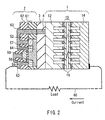
- FIG. 2 is a cross-sectional view schematically illustrating another example of a semiconductor device of the present invention.
- the semiconductor device shown in FIG. 2 includes a fuel cell 1 and a semiconductor element 2.
- the fuel cell 1 includes an anode separator 12, a cathode separator 14, and a MEA 15 that is interposed between the anode separator 12 and the cathode separator 14.
- contact layers 16 are arranged between the respective separators and the MEA 15, so that electric power generated by the MEA 15 can be collected more efficiently.
- the semiconductor element 2 is formed on an insulation layer 3 arranged on one of principal surfaces of the anode separator 12 so that the semiconductor element 2 and the anode separator 12 are connected electrically with each other via an electrode 4 formed in the insulation layer 3.
- the semiconductor element 2 is a N-channel MOS transistor that includes a P-well contact layer 52, a N-type drain electrode 56, a N-type source electrode 57, gate insulation films 58, a N-type gate electrode 59, an element separation insulation film 61, interlayer insulation films 62, element wiring 63, and a P-well 64.
- the source electrode and a substrate electrode of the foregoing N-channel MOS transistor are connected electrically with the anode separator 12 via an electrode 4, and the drain electrode and the gate electrode of the same are connected electrically with the cathode separator 14 via external wiring 66.
- an external load is connected to which power generated by the fuel cell 1 is supplied.
- the transistor in the case where an output voltage of the fuel cell 1 is not lower than a threshold voltage of the N-channel MOS transistor, the transistor is ON permanently and is capable of supplying power to the external load. However, when the output voltage of the fuel cell 1 is not higher than the threshold voltage, the transistor is turned OFF, and the power supply to the external load is stopped.
- the foregoing threshold value is set to a lower limit voltage of the fuel cell (the lowest voltage that the fuel cell generates power safely), it is possible to prevent a malfunction of an electronic device due to a problem of the fuel cell or damage occurring to the fuel cell due to an excessive decrease in the voltage of the fuel cell.
- the semiconductor device can be made to have a function as a limiter with respect to the output current of the fuel cell 1.
- the threshold voltage of the transistor can be controlled by adjusting the concentration of an impurity diffused in the P-well 64, a thickness of the gate insulation film 58, and a material (work function) of the N-type gate electrode 59.
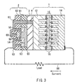
- FIG. 3 is a schematic cross-sectional view illustrating still another example of a semiconductor device of the present invention.
- the semiconductor device shown in FIG. 3 is a modification of the semiconductor device shown in FIG. 2 in which the semiconductor element 2 is changed from the N-channel MOS transistor to a P-channel MOS transistor.
- the semiconductor element 2 shown in FIG. 3 is a P-channel MOS transistor that includes a N-well contact layer 53, a P-type source electrode 54, a P-type drain electrode 55, gate insulation films 58, a P-type gate electrode 60, an element separation insulation film 61, interlayer insulation films 62, element wiring 63, and a N-well 65.
- the source electrode and the gate electrode of the foregoing P-channel MOS transistor are connected electrically with the anode separator 12 via an electrode 4, and the drain electrode and a substrate electrode of the same are connected electrically with the cathode separator 14 via external wiring 66.
- an external load is connected to which power generated by the fuel cell 1 is supplied.
- an output voltage of a single cell of the PEFC type normally is not more than approximately 1 V
- an interface circuit DC-DC converter circuit, etc.
- a control circuit for controlling an output of the fuel cell voltage control circuit, current control circuit, etc.
- the fuel cell and a semiconductor element including the foregoing circuit are provided integrally so as to be able to provide the semiconductor device having more excellent compactness and versatility, as in the semiconductor device according to the present embodiment.
- FIG. 4A is a cross-sectional view schematically illustrating an example of a fuel cell in a semiconductor device of the present invention.
- a fuel cell 1 shown in FIG. 4A includes an anode separator 12, a cathode separator 14, and a MEA 15 that is interposed between the anode separator 12 and the cathode separator 14. Openings 17 are provided in the cathode separator 14 so that flow channels of the cathode separator 14 are opened to the atmosphere.
- FIG. 4B is a schematic view of the fuel cell 1 shown in FIG. 4A viewed in a direction indicated by an arrow X shown in FIG. 4A.
- FIG. 4C is an enlarged schematic view of a part of the openings 17 shown in FIG. 4B (encircled part in FIG. 4B).
- portions denoted with "Y" in FIG. 4C are portions actually opened, and thus, air is supplied to the cathode of the MEA through the portions Y.
- the width and length of the openings 17, the size of the portions Y shown in FIG. 4C in the case where each opening 17 is formed in a lattice form, the number of the portions Y included in each opening 17, etc. are not limited particularly. They may be set appropriately according to the size of the cathode separator and required characteristics of the cell. To prevent usual foreign matters from entering the flow channels, an area of the opened portion Y may be set in a range of, for instance, 100 ⁇ m 2 to 1000 ⁇ m 2 . For instance, in the case where each opening 17 has a width of 200 ⁇ m, the area of the opened portion Y may be set to be 100 ⁇ m 2 , and a space between adjacent portions Y may be set to be 5 ⁇ m. Further, the thickness of a portion that is processed in a lattice form may be set appropriately.
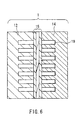
- FIG. 5 is a schematic cross-sectional view illustrating another example of a fuel cell in a semiconductor device of the present invention.
- a fuel cell 1 shown in FIG. 5 is configured by stacking a plurality of single cells, each including an anode separator 12, a cathode separator 14, and a MEA 15. Further, in the fuel cell 1 shown in FIG. 5, the anode separators and the cathode separators except for separators at both ends are configured so that each pair of adjacent anode and cathode separators are integrated with each other, thereby forming a separator 18. Flow channels 11 for fuel are formed on one of principal surface of each separator 18, and flow channels 13 for oxidizer are formed on the other principal surface thereof opposite to the foregoing principal surface. The separator 18 serves as both of the anode separator and the cathode separator, and the single-cells are connected in series via the separators 18.
- This configuration of a fuel cell can increase an output voltage while keeping an electric generation area of the cell unchanged. For instance, in the example shown in FIG. 5, since three cells are connected in series, an output voltage of the fuel cell increases to approximately three times that of a single cell. Further, the provision of a fuel cell in which single-cells are stacked can render the semiconductor device more excellent versatility. It should be noted that the number of stacked single-cells is not limited to three as in the example shown in FIG. 5, and may be set appropriately according to the required electric power generation characteristics.
- separators 18 each of which is formed by integrating an anode separator and a cathode separator as shown in FIG. 5.
- separators 18 may be stacked simply.
- layers for cooling the fuel cell may be arranged between adjacent single-cells.
- materials used in respective parts of the fuel cell according to the present embodiment, thicknesses and sizes of the respective parts thereof, etc. are the same as those of the first embodiment described above.
- FIG. 6 is a cross-sectional view illustrating still another example of a fuel cell in a semiconductor device of the present invention.
- a fuel cell 1 shown in FIG. 6 includes an anode separator 12, a cathode separator 14, and a MEA 15 interposed between the anode separator 12 and the cathode separator 14. Further, water-repellent layers 19 are formed on flow channels for oxidizer in the cathode separator 14.
- the configuration of the water-repellent layers 19 is not limited particularly, as long as a water-repellent effect can be achieved. They may be formed by, for instance, forming HMDS (hexamethyldisilazane) layers by spin coating on the flow channels in the separator. Furthermore, in the case where a separator is formed with a semiconductor substrate made of crystalline silicon, water-repellent layers may be formed by projection of a laser beam or heat treatment in ultrahigh vacuum. In this case, projections and recesses of the several nanometers order are formed on a surface of the crystalline silicon by a laser beam or the like, and the water repellency can be achieved by the foregoing projections and recesses.
- HMDS hexamethyldisilazane
- water-repellent layers are formed only in the cathode separator 14 in the fuel cell 1 shown in FIG. 6, they may be formed in the anode separator 12 also. Further, materials used in respective parts of the fuel cell according to the present embodiment, thicknesses and sizes of the respective parts thereof, etc. are the same as those of the first embodiment described above.
- the method for producing a semiconductor device of the present invention is a method for producing a semiconductor device including a fuel cell that has a structure in which a MEA is interposed between a pair of separators.
- the method includes the steps of:
- This producing method can be implemented by a semiconductor processing process. Therefore, it is possible to produce, with improved productivity, a compact semiconductor device with excellent versatility in which a fuel cell and a semiconductor element are integrated. Further, in the case where a large-diameter silicon wafer is used as a semiconductor substrate, a number of semiconductor devices can be produced at a time. This makes it possible to produce a semiconductor device at a lower cost.
- the semiconductor substrate may include an insulation layer between the first and second surfaces thereof.
- step (i) may include a sub-step of:
- the producing method described below is a method for producing a semiconductor device in which a semiconductor element is formed on an anode separator, but this also applies to a case of a semiconductor device in which a semiconductor element is formed on a cathode separator.
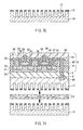
- a laminate in which a semiconductor substrate 7, an insulation layer 3, and a crystalline silicon layer 8 are laminated is formed (FIG. 7A).
- the foregoing laminate may be formed by depositing the respective layers, but a SOI substrate available in the market (for instance, a UNIBOND substrate manufactured by Silicon-On-Insulator Technologies (SOITEC)) may be used. Respective thicknesses of the foregoing layers may be set appropriately according to characteristics that the semiconductor device is required to have. Since the semiconductor substrate 7 finally becomes an anode separator, the materials thereof may be the same materials as those for the semiconductor substrate for use in the anode separator in the first embodiment.
- the semiconductor substrate 7 may have a N-type conductivity, a plane direction (001), an orientation flat plane direction ⁇ 110>, a specific resistance of 10 m ⁇ cm, and a thickness of 650 ⁇ m.
- the insulation layer 3 may be made of SiO 2 , and have a thickness of 400 nm.
- the crystalline silicon layer 8 has a thickness of 200 nm.
- a semiconductor element 2 is formed on the crystalline silicon layer 8 formed on the insulation layer 3 (FIG. 7B).
- the CMOS inverter shown in FIG. 1 is formed as the semiconductor element 2.
- Respective parts of the semiconductor element 2 shown in FIG. 7B basically are identical to those of the semiconductor element 2 shown in FIG. 1, and the same parts are indicated by the same reference numerals.
- the semiconductor element 2 as that shown in FIG. 7B further includes a passivation film 67 composed of a silicon nitride film formed by plasma CVD or the like, and further, an opening 68 for later connection with external wiring is provided.
- an electrode 4 for electrical connection between the semiconductor element 2 and the semiconductor substrate 7 is formed in an insulation layer 3, and a contact layer 69 is arranged so as to reduce a contact resistance between the electrode 4 and the semiconductor substrate 7.
- CMOS inverter forming process As a process for forming the semiconductor element 2 on the insulation layer 3, a usual semiconductor element forming process (a CMOS inverter forming process in the case of the example shown in FIG. 7B) may be used. Further, the materials used in the first embodiment may be used for forming the respective parts of the semiconductor element 2 and the contact layer 69. The electrode 4 and the element wiring 63 may be formed integrally.
- the flow channels 11 for fuel are formed through the following steps on a surface of the semiconductor substrate 7 opposite to the foregoing surface thereof on which the insulation layer 3 and the semiconductor element 2 are formed.
- the foregoing laminate is immersed in approximately 5 wt% diluted hydrogen fluoride solution for approximately 30 seconds so that a natural oxide film on the semiconductor substrate 7 is removed. Then, ion implantation with accelerated As atoms (for instance, implantation at an acceleration voltage in a range of 10 keV to 100 keV and a dose in a range of 10 14 cm -2 to 10 16 cm -2 ) is carried out with respect to the surface of the semiconductor substrate 7 that is opposite to the surface having the semiconductor element 2 and the insulation layer 3 thereon, and further, a rapid heating (for instance, at 200°C during one minute) is carried out. By so doing, a degenerated As-diffused layer 70 having a N-type conductivity is formed (FIG. 7C).
- the As-diffused layer 70 has a thickness in a range of, for instance, 0.01 ⁇ m to 10 ⁇ m, preferably 0.01 ⁇ m to 0.5 ⁇ m.
- nickel is deposited by sputtering or vacuum deposition to form a film on the As-diffused layer 70, and further, a rapid heating (for instance, at 400°C during one minute, however the heating temperature being set to be lower than a melting point of element wiring 43 within the semiconductor element 2), whereby a nickel silicide film 71 is formed (FIG. 7D).
- a laminate film of the As-diffused layer 70 and the nickel silicide film 71 constitutes a contact layer 16.
- the composition of the contact layer 16 can be controlled.
- the thickness of a nickel film to be deposited is in a range of, for instance, 0.01 ⁇ m to 10 ⁇ m, preferably in a range of 0.01 ⁇ m to 0.5 ⁇ m.
- a nickel silicide film having a thickness in a range of 0.01 ⁇ m to 10 ⁇ m (or 0.01 ⁇ m to 0.5 ⁇ m) can be formed.
- a resist pattern 72 (thickness: for instance, 30 ⁇ m) that is matched with a pattern of flow channels to be formed is formed on the contact layer 16 (FIG. 7E), and thereafter, flow channels for fuel are formed on the semiconductor substrate 7 by dry etching or the like.
- widths and depths of the flow channels for fuel can be controlled.
- an anode separator 12 is obtained that has the insulation layer 3 and the semiconductor element 2 on one of principal surfaces thereof and the flow channels 11 for fuel on the surface opposite to the foregoing principal surface (FIG. 7F).
- a cathode separator 14 on which flow channels 13 for oxidizer and a contact layer 16 are formed is formed by the same method as that shown in FIGS. 7C to 7F (FIG. 7G).
- the formation of the cathode separator 14 may start with, for instance, a step of forming an impurity-diffused layer on a single-layer semiconductor substrate.
- anode separator 12 thus prepared as described above, the cathode separator 14, and an MEA 15 separately prepared are laminated so that surfaces of the separators on which flow channels are formed are brought into contact with the MEA 15 (FIG. 7H).
- pressure or heat may be applied as required, or the entirety may be covered with a resin or the like.
- the cathode separator 14 and the semiconductor element 2 are connected with each other via external wiring, whereby a semiconductor device as shown in FIG. 1 is obtained.
- the formation of the semiconductor element and the formation of the flow channels for fuel may be carried out in a reversed order (i.e., the semiconductor element may be formed after the flow channels for fuel are formed).
- the present invention can provide a further compact and versatile semiconductor device equipped with a fuel cell. Further, the present invention also provides a method for producing a semiconductor device equipped with a fuel cell, which is capable of producing a semiconductor device equipped with the fuel cell with improved productivity.
- the semiconductor device of the present invention can be used in an electronic circuit device, a power source, a light source, a micromachine, a microsensor, etc.
Landscapes
- Chemical & Material Sciences (AREA)
- Chemical Kinetics & Catalysis (AREA)
- Electrochemistry (AREA)
- General Chemical & Material Sciences (AREA)
- Life Sciences & Earth Sciences (AREA)
- Engineering & Computer Science (AREA)
- Manufacturing & Machinery (AREA)
- Sustainable Development (AREA)
- Sustainable Energy (AREA)
- Fuel Cell (AREA)
- Internal Circuitry In Semiconductor Integrated Circuit Devices (AREA)
- Seeds, Soups, And Other Foods (AREA)
Abstract
Description
Claims (25)
- A semiconductor device equipped with a fuel cell, the semiconductor device comprising a fuel cell and a semiconductor element,
wherein
the fuel cell includes an anode separator in which a flow channel for fuel is formed, a cathode separator in which a flow channel for oxidizer is formed, and a membrane electrode assembly interposed between the anode separator and the cathode separator,
the semiconductor element is formed on a principal surface of one separator selected from the anode separator and the cathode separator, and
the semiconductor element and the selected separator are connected electrically. - The semiconductor device according to claim 1,
wherein two of the semiconductor elements are included, the semiconductor elements being a first semiconductor element formed on a principal surface of the anode separator, and a second semiconductor element formed on a principal surface of the cathode separator. - The semiconductor device according to claim 1,
wherein the selected separator is formed with a semiconductor substrate. - The semiconductor device according to claim 3,
wherein the semiconductor substrate is made of crystalline silicon. - The semiconductor device according to claim 3,
wherein the semiconductor substrate is made of a compound semiconductor containing an element of the group IIIb and an element of the group Vb. - The semiconductor device according to claim 3,
wherein the semiconductor substrate is made of a compound semiconductor containing an element of the group IIb and an element of the group VIb. - The semiconductor device according to claim 3,
wherein the anode separator is formed with a N-type semiconductor substrate and the cathode separator is formed with a P-type semiconductor substrate. - The semiconductor device according to claim 3,
wherein the fuel cell further includes a contact layer arranged between the selected separator and the membrane electrode assembly so as to reduce a contact resistance between the selected separator and the membrane electrode assembly. - The semiconductor device according to claim 1,
wherein the fuel cell further includes an insulation layer formed between the semiconductor element and the selected separator. - The semiconductor device according to claim 9,
wherein the semiconductor element is connected electrically with the selected separator via an electrode formed in the insulation layer. - The semiconductor device according to claim 9,
wherein the insulation layer is made of SiO2. - The semiconductor device according to claim 9,
wherein the insulation layer has a specific resistance of not less than 105 Ω·cm. - The semiconductor device according to claim 9,
wherein the insulation layer has a thickness in a range of 10 nm to 1 µm. - The semiconductor device according to claim 9,
wherein the selected separator is made of a metal. - The semiconductor device according to claim 14,
wherein the insulation layer is a metal oxide film. - The semiconductor device according to claim 1,
wherein
the semiconductor element includes a first electrode and a second electrode,
the first electrode is connected electrically with the anode separator, and
the second electrode is connected electrically with the cathode separator. - The semiconductor device according to claim 1,
wherein
the semiconductor element is a N-channel MOS transistor,
a source electrode and a substrate electrode of the N-channel MOS transistor are connected electrically with the anode separator, and
a drain electrode and a gate electrode of the N-channel MOS transistor are connected electrically with the cathode separator. - The semiconductor device according to claim 1,
wherein
the semiconductor element is a P-channel MOS transistor,
a source electrode and a gate electrode of the P-channel MOS transistor are connected electrically with the anode separator, and
a drain electrode and a substrate electrode of the P-channel MOS transistor are connected electrically with the cathode separator. - The semiconductor device according to claim 1,
wherein the fuel cell is formed by stacking a plurality of cells, each cell including the anode separator, the cathode separator, and the membrane electrode assembly. - A method for producing a semiconductor device equipped with a fuel cell having a structure in which a membrane electrode assembly is interposed between a pair of separators, the method comprising the steps of:(i) forming a semiconductor element on one surface of a semiconductor substrate;(ii) forming a flow channel through which either fuel or oxidizer is to flow on a surface of the semiconductor substrate that is opposite to the surface on which the semiconductor element is formed; and(iii) laminating the membrane electrode assembly on the semiconductor substrate so that the surface of the semiconductor substrate with the flow channel thereon is in contact with the membrane electrode assembly, wherein the semiconductor substrate serves as one separator selected from the pair of separators.
- The method according to claim 20,
wherein the semiconductor substrate includes an insulation layer between the surface with the semiconductor element thereon and the surface with the flow channel thereon. - The method according to claim 21,
wherein the step (i) includes a sub-step of(a) forming the semiconductor element on the insulation layer in a manner such that the semiconductor element and the semiconductor substrate are connected electrically with each other via an electrode formed in the insulation layer. - A method for producing a semiconductor device equipped with a fuel cell having a structure in which a membrane electrode assembly is interposed between a pair of separators, the method comprising the steps of:(I) forming a flow channel through which either fuel or oxidizer is to flow on a surface of the semiconductor substrate;(II) forming a semiconductor element on a surface of the semiconductor substrate that is opposite to the surface on which the flow channel is formed; and(III) laminating the membrane electrode assembly on the semiconductor substrate so that the surface of the semiconductor substrate with the flow channel thereon is in contact with the membrane electrode assembly, wherein the semiconductor substrate serves as one separator selected from the pair of separators.
- The method according to claim 23,
wherein the semiconductor substrate includes an insulation layer between the surface with the flow channel thereon and the surface with the semiconductor element thereon. - The method according to claim 24,
wherein the step (II) includes a sub-step of:(A) forming the semiconductor element on the insulation layer in a manner such that the semiconductor element and the semiconductor substrate are connected electrically with each other via an electrode formed in the insulation layer.
Applications Claiming Priority (3)
| Application Number | Priority Date | Filing Date | Title |
|---|---|---|---|
| JP2002019659 | 2002-01-29 | ||
| JP2002019659 | 2002-01-29 | ||
| PCT/JP2003/000618 WO2003065487A1 (en) | 2002-01-29 | 2003-01-23 | Semiconductor device having fuel cell and its manufacturing method |
Publications (3)
| Publication Number | Publication Date |
|---|---|
| EP1471588A1 true EP1471588A1 (en) | 2004-10-27 |
| EP1471588A4 EP1471588A4 (en) | 2007-01-03 |
| EP1471588B1 EP1471588B1 (en) | 2008-07-23 |
Family
ID=27654272
Family Applications (1)
| Application Number | Title | Priority Date | Filing Date |
|---|---|---|---|
| EP03703040A Expired - Lifetime EP1471588B1 (en) | 2002-01-29 | 2003-01-23 | Semiconductor device having fuel cell and its manufacturing method |
Country Status (7)
| Country | Link |
|---|---|
| US (1) | US6933570B2 (en) |
| EP (1) | EP1471588B1 (en) |
| JP (1) | JP3700979B2 (en) |
| CN (1) | CN1328811C (en) |
| AT (1) | ATE402484T1 (en) |
| DE (1) | DE60322342D1 (en) |
| WO (1) | WO2003065487A1 (en) |
Cited By (1)
| Publication number | Priority date | Publication date | Assignee | Title |
|---|---|---|---|---|
| EP1843422A1 (en) * | 2006-04-06 | 2007-10-10 | STMicroelectronics S.r.l. | Method and circuit for managing a start-up phase of at least a micro fuel cell to be connected to a load |
Families Citing this family (19)
| Publication number | Priority date | Publication date | Assignee | Title |
|---|---|---|---|---|
| US20120264024A1 (en) * | 1999-04-29 | 2012-10-18 | Pelton Walter E | Methods and apparatuses for electrochemical cell system with movable medium and non-conducting substrate |
| CN1328811C (en) * | 2002-01-29 | 2007-07-25 | 松下电器产业株式会社 | Semiconductor device having fuel cell and its manufacturing method |
| US20080233436A1 (en) * | 2003-07-28 | 2008-09-25 | General Motors Corporation | Diffusion media tailored to account for variations in operating humidity and devices incorporating the same |
| US7235315B2 (en) * | 2003-12-16 | 2007-06-26 | Ballard Power Systems Inc. | Electrochemical fuel cell stack having a plurality of integrated voltage reversal protection diodes |
| KR101065375B1 (en) * | 2004-06-23 | 2011-09-16 | 삼성에스디아이 주식회사 | Bipolar plate for fuel cell, manufacturing method thereof and fuel cell comprising same |
| US7842435B2 (en) * | 2004-11-01 | 2010-11-30 | Gm Global Technology Operations, Inc. | Fuel cell water management enhancement method |
| US8486551B2 (en) * | 2005-09-29 | 2013-07-16 | Micro Silitron Inc. | Fuel cell unit, fuel cell unit array, fuel cell module and fuel cell system |
| KR100673616B1 (en) * | 2005-12-05 | 2007-01-24 | 경상대학교산학협력단 | Semiconductor Silicon Wafer with Power Supply on Wafer Back |
| JP5234878B2 (en) * | 2006-02-22 | 2013-07-10 | 独立行政法人産業技術総合研究所 | Fuel cell |
| US20070243452A1 (en) * | 2006-04-14 | 2007-10-18 | Applied Materials, Inc. | Reliable fuel cell electrode design |
| KR100645594B1 (en) | 2006-07-12 | 2006-11-15 | 한국에너지기술연구원 | Cell or stack for fuel cell performance evaluation and method for evaluating fuel cell performance |
| US20080093633A1 (en) * | 2006-10-18 | 2008-04-24 | United Microelectronics Corp. | Complementary metal-oxide-semiconductor (cmos) image sensor and fabricating method thereof |
| JP2008159447A (en) * | 2006-12-25 | 2008-07-10 | Shinko Electric Ind Co Ltd | Solid oxide fuel cell power generator |
| KR20090119187A (en) * | 2008-05-15 | 2009-11-19 | 삼성전자주식회사 | Packages comprising fuel cells, methods of manufacturing the same, and cards and systems comprising the packages |
| JP5610562B2 (en) * | 2008-11-05 | 2014-10-22 | 神奈川県 | Fuel cell and manufacturing method thereof |
| KR101829176B1 (en) * | 2009-11-20 | 2018-02-13 | 가부시키가이샤 한도오따이 에네루기 켄큐쇼 | Semiconductor device |
| TWI688047B (en) * | 2010-08-06 | 2020-03-11 | 半導體能源研究所股份有限公司 | Semiconductor device |
| KR102371046B1 (en) * | 2016-07-15 | 2022-03-07 | 현대자동차주식회사 | End cell heater for fuel cell |
| EP3806215A4 (en) | 2018-06-07 | 2022-03-16 | Sunland (Shanghai) Investment Co. Ltd | SILICON POLE PLATE AND METHOD OF PRODUCTION THEREOF, USE OF SILICON IN A FUEL CELL, FUEL CELL STACK STRUCTURE, FUEL CELL AND USE THEREOF |
Family Cites Families (16)
| Publication number | Priority date | Publication date | Assignee | Title |
|---|---|---|---|---|
| JPH0650783B2 (en) * | 1982-03-29 | 1994-06-29 | 株式会社半導体エネルギ−研究所 | Photovoltaic device |
| JP3339730B2 (en) | 1992-12-24 | 2002-10-28 | 忠弘 大見 | Semiconductor device |
| JP3503197B2 (en) * | 1994-07-04 | 2004-03-02 | 株式会社デンソー | Semiconductor device |
| JP3401918B2 (en) | 1994-07-04 | 2003-04-28 | 株式会社デンソー | Semiconductor device |
| KR100253699B1 (en) | 1996-06-29 | 2000-05-01 | 김영환 | Soi device and its manufacturing method |
| EP0895282A3 (en) * | 1997-07-30 | 2000-01-26 | Canon Kabushiki Kaisha | Method of preparing a SOI substrate by using a bonding process, and SOI substrate produced by the same |
| JP4623451B2 (en) | 1997-07-30 | 2011-02-02 | 忠弘 大見 | Semiconductor substrate and manufacturing method thereof |
| US6638654B2 (en) * | 1999-02-01 | 2003-10-28 | The Regents Of The University Of California | MEMS-based thin-film fuel cells |
| CN1117882C (en) * | 1999-04-19 | 2003-08-13 | 住友金属工业株式会社 | Stainless steel material for solid polymer fuel battery |
| CA2370899A1 (en) * | 1999-05-06 | 2000-11-16 | Sandia Corporation | Fuel cell and membrane |
| US6312846B1 (en) * | 1999-11-24 | 2001-11-06 | Integrated Fuel Cell Technologies, Inc. | Fuel cell and power chip technology |
| WO2001080286A2 (en) * | 2000-04-17 | 2001-10-25 | The Penn State Research Foundation | Deposited thin films and their use in separation and sarcrificial layer applications |
| DE10021907B4 (en) * | 2000-05-05 | 2005-06-02 | Ballard Power Systems Ag | Fuel cell system with a fuel cell stack with integrated polarity reversal protection diode |
| JP2002075399A (en) * | 2000-08-30 | 2002-03-15 | Hitachi Ltd | Solid polymer electrolyte fuel cell separator |
| EP1258937A1 (en) * | 2001-05-17 | 2002-11-20 | STMicroelectronics S.r.l. | Micro silicon fuel cell, method of fabrication and self-powered semiconductor device integrating a micro fuel cell |
| CN1328811C (en) * | 2002-01-29 | 2007-07-25 | 松下电器产业株式会社 | Semiconductor device having fuel cell and its manufacturing method |
-
2003
- 2003-01-23 CN CNB038029456A patent/CN1328811C/en not_active Expired - Fee Related
- 2003-01-23 DE DE60322342T patent/DE60322342D1/en not_active Expired - Fee Related
- 2003-01-23 EP EP03703040A patent/EP1471588B1/en not_active Expired - Lifetime
- 2003-01-23 AT AT03703040T patent/ATE402484T1/en not_active IP Right Cessation
- 2003-01-23 WO PCT/JP2003/000618 patent/WO2003065487A1/en not_active Ceased
- 2003-01-23 JP JP2003564966A patent/JP3700979B2/en not_active Expired - Fee Related
- 2003-10-28 US US10/696,347 patent/US6933570B2/en not_active Expired - Fee Related
Cited By (2)
| Publication number | Priority date | Publication date | Assignee | Title |
|---|---|---|---|---|
| EP1843422A1 (en) * | 2006-04-06 | 2007-10-10 | STMicroelectronics S.r.l. | Method and circuit for managing a start-up phase of at least a micro fuel cell to be connected to a load |
| US7906874B2 (en) | 2006-04-06 | 2011-03-15 | Stmicroelectronics S.R.L. | Method and circuit for managing start-up phase of at least a micro fuel cell to be connected to a load |
Also Published As
| Publication number | Publication date |
|---|---|
| US6933570B2 (en) | 2005-08-23 |
| US20040099907A1 (en) | 2004-05-27 |
| JPWO2003065487A1 (en) | 2005-05-26 |
| EP1471588B1 (en) | 2008-07-23 |
| CN1328811C (en) | 2007-07-25 |
| ATE402484T1 (en) | 2008-08-15 |
| CN1625818A (en) | 2005-06-08 |
| WO2003065487A1 (en) | 2003-08-07 |
| JP3700979B2 (en) | 2005-09-28 |
| DE60322342D1 (en) | 2008-09-04 |
| EP1471588A4 (en) | 2007-01-03 |
Similar Documents
| Publication | Publication Date | Title |
|---|---|---|
| EP1471588B1 (en) | Semiconductor device having fuel cell and its manufacturing method | |
| JP5213134B2 (en) | Solar cell | |
| US20040258984A1 (en) | Integrated thin film batteries on silicon integrated circuits | |
| JP4573594B2 (en) | Secondary battery | |
| EP1999814A2 (en) | Integrated micro fuel cell apparatus | |
| CN102290485A (en) | Method of fabricating thin film solar cell | |
| TW200947726A (en) | Buried insulator isolation for solar cell contacts | |
| CN120500117A (en) | Solar cell and photovoltaic module | |
| TW201937748A (en) | Method for producing solar cell | |
| WO2023015994A1 (en) | Perovskite material bypass diode and preparation method therefor, perovskite solar cell module and preparation method therefor, and photovoltaic module | |
| TW201007958A (en) | Photovoltaic cell comprising a thin lamina having a rear junction and method of making | |
| US8242590B2 (en) | Silicon wafer for semiconductor with powersupply system on the backside of wafer | |
| CN102315325A (en) | The formation method of the conductive area of reducing in the transparent conductive film of photovoltaic module | |
| CN112054024B (en) | Field effect transistor device, preparation method and battery management system | |
| US11646451B2 (en) | Semiconductor device, manufacturing method thereof, and power generating device | |
| JP2003282089A (en) | Micro fuel cell | |
| CN119384006A (en) | Semiconductor device and manufacturing method, power module, power conversion circuit and vehicle | |
| JPH0377382A (en) | Solar battery cell | |
| CN114093899B (en) | Detector integrated with solar cell and manufacturing method thereof | |
| JP5224470B2 (en) | Photoelectric conversion member | |
| JPS5910593B2 (en) | Method of manufacturing photovoltaic device | |
| US8952473B2 (en) | Integrated circuit combination of a target integrated circuit and a plurality of cells connected thereto using the top conductive layer | |
| CN121531729A (en) | A low-voltage, low-clamping, low-leakage transient suppression diode and its fabrication method | |
| CN103762219B (en) | Series boosting solar battery cell and preparation method thereof | |
| CN118315431A (en) | A SiC MOSFET device and manufacturing method thereof |
Legal Events
| Date | Code | Title | Description |
|---|---|---|---|
| PUAI | Public reference made under article 153(3) epc to a published international application that has entered the european phase |
Free format text: ORIGINAL CODE: 0009012 |
|
| 17P | Request for examination filed |
Effective date: 20030801 |
|
| AK | Designated contracting states |
Kind code of ref document: A1 Designated state(s): AT BE BG CH CY CZ DE DK EE ES FI FR GB GR HU IE IT LI LU MC NL PT SE SI SK TR |
|
| AX | Request for extension of the european patent |
Extension state: AL LT LV MK RO |
|
| A4 | Supplementary search report drawn up and despatched |
Effective date: 20061204 |
|
| RIC1 | Information provided on ipc code assigned before grant |
Ipc: H01M 8/10 20060101ALI20061128BHEP Ipc: H01L 23/58 20060101AFI20061128BHEP Ipc: H01L 27/06 20060101ALI20061128BHEP |
|
| 17Q | First examination report despatched |
Effective date: 20070906 |
|
| GRAP | Despatch of communication of intention to grant a patent |
Free format text: ORIGINAL CODE: EPIDOSNIGR1 |
|
| GRAS | Grant fee paid |
Free format text: ORIGINAL CODE: EPIDOSNIGR3 |
|
| GRAA | (expected) grant |
Free format text: ORIGINAL CODE: 0009210 |
|
| AK | Designated contracting states |
Kind code of ref document: B1 Designated state(s): AT BE BG CH CY CZ DE DK EE ES FI FR GB GR HU IE IT LI LU MC NL PT SE SI SK TR |
|
| REG | Reference to a national code |
Ref country code: GB Ref legal event code: FG4D |
|
| REG | Reference to a national code |
Ref country code: CH Ref legal event code: EP |
|
| REG | Reference to a national code |
Ref country code: IE Ref legal event code: FG4D |
|
| REF | Corresponds to: |
Ref document number: 60322342 Country of ref document: DE Date of ref document: 20080904 Kind code of ref document: P |
|
| RAP2 | Party data changed (patent owner data changed or rights of a patent transferred) |
Owner name: PANASONIC CORPORATION |
|
| REG | Reference to a national code |
Ref country code: CH Ref legal event code: PFA Owner name: PANASONIC CORPORATION Free format text: MATSUSHITA ELECTRIC INDUSTRIAL CO., LTD.#1006, OAZA-KADOMA#KADOMA-SHI, OSAKA 571-8501 (JP) -TRANSFER TO- PANASONIC CORPORATION#1006, OAZA KADOMA, KADOMA-SHI#OSAKA 571-8501 (JP) |
|
| NLV1 | Nl: lapsed or annulled due to failure to fulfill the requirements of art. 29p and 29m of the patents act | ||
| PG25 | Lapsed in a contracting state [announced via postgrant information from national office to epo] |
Ref country code: PT Free format text: LAPSE BECAUSE OF FAILURE TO SUBMIT A TRANSLATION OF THE DESCRIPTION OR TO PAY THE FEE WITHIN THE PRESCRIBED TIME-LIMIT Effective date: 20081223 Ref country code: NL Free format text: LAPSE BECAUSE OF FAILURE TO SUBMIT A TRANSLATION OF THE DESCRIPTION OR TO PAY THE FEE WITHIN THE PRESCRIBED TIME-LIMIT Effective date: 20080723 Ref country code: ES Free format text: LAPSE BECAUSE OF FAILURE TO SUBMIT A TRANSLATION OF THE DESCRIPTION OR TO PAY THE FEE WITHIN THE PRESCRIBED TIME-LIMIT Effective date: 20081103 |
|
| PG25 | Lapsed in a contracting state [announced via postgrant information from national office to epo] |
Ref country code: SI Free format text: LAPSE BECAUSE OF FAILURE TO SUBMIT A TRANSLATION OF THE DESCRIPTION OR TO PAY THE FEE WITHIN THE PRESCRIBED TIME-LIMIT Effective date: 20080723 Ref country code: FI Free format text: LAPSE BECAUSE OF FAILURE TO SUBMIT A TRANSLATION OF THE DESCRIPTION OR TO PAY THE FEE WITHIN THE PRESCRIBED TIME-LIMIT Effective date: 20080723 Ref country code: BG Free format text: LAPSE BECAUSE OF FAILURE TO SUBMIT A TRANSLATION OF THE DESCRIPTION OR TO PAY THE FEE WITHIN THE PRESCRIBED TIME-LIMIT Effective date: 20081023 Ref country code: AT Free format text: LAPSE BECAUSE OF FAILURE TO SUBMIT A TRANSLATION OF THE DESCRIPTION OR TO PAY THE FEE WITHIN THE PRESCRIBED TIME-LIMIT Effective date: 20080723 |
|
| PG25 | Lapsed in a contracting state [announced via postgrant information from national office to epo] |
Ref country code: BE Free format text: LAPSE BECAUSE OF FAILURE TO SUBMIT A TRANSLATION OF THE DESCRIPTION OR TO PAY THE FEE WITHIN THE PRESCRIBED TIME-LIMIT Effective date: 20080723 |
|
| PG25 | Lapsed in a contracting state [announced via postgrant information from national office to epo] |
Ref country code: DK Free format text: LAPSE BECAUSE OF FAILURE TO SUBMIT A TRANSLATION OF THE DESCRIPTION OR TO PAY THE FEE WITHIN THE PRESCRIBED TIME-LIMIT Effective date: 20080723 Ref country code: EE Free format text: LAPSE BECAUSE OF FAILURE TO SUBMIT A TRANSLATION OF THE DESCRIPTION OR TO PAY THE FEE WITHIN THE PRESCRIBED TIME-LIMIT Effective date: 20080723 |
|
| PG25 | Lapsed in a contracting state [announced via postgrant information from national office to epo] |
Ref country code: SK Free format text: LAPSE BECAUSE OF FAILURE TO SUBMIT A TRANSLATION OF THE DESCRIPTION OR TO PAY THE FEE WITHIN THE PRESCRIBED TIME-LIMIT Effective date: 20080723 Ref country code: CZ Free format text: LAPSE BECAUSE OF FAILURE TO SUBMIT A TRANSLATION OF THE DESCRIPTION OR TO PAY THE FEE WITHIN THE PRESCRIBED TIME-LIMIT Effective date: 20080723 |
|
| PGFP | Annual fee paid to national office [announced via postgrant information from national office to epo] |
Ref country code: DE Payment date: 20090127 Year of fee payment: 7 |
|
| PLBE | No opposition filed within time limit |
Free format text: ORIGINAL CODE: 0009261 |
|
| STAA | Information on the status of an ep patent application or granted ep patent |
Free format text: STATUS: NO OPPOSITION FILED WITHIN TIME LIMIT |
|
| PGFP | Annual fee paid to national office [announced via postgrant information from national office to epo] |
Ref country code: GB Payment date: 20090113 Year of fee payment: 7 |
|
| 26N | No opposition filed |
Effective date: 20090424 |
|
| PG25 | Lapsed in a contracting state [announced via postgrant information from national office to epo] |
Ref country code: MC Free format text: LAPSE BECAUSE OF NON-PAYMENT OF DUE FEES Effective date: 20090131 Ref country code: IT Free format text: LAPSE BECAUSE OF FAILURE TO SUBMIT A TRANSLATION OF THE DESCRIPTION OR TO PAY THE FEE WITHIN THE PRESCRIBED TIME-LIMIT Effective date: 20080723 |
|
| REG | Reference to a national code |
Ref country code: CH Ref legal event code: PL |
|
| PG25 | Lapsed in a contracting state [announced via postgrant information from national office to epo] |
Ref country code: CH Free format text: LAPSE BECAUSE OF NON-PAYMENT OF DUE FEES Effective date: 20090131 Ref country code: LI Free format text: LAPSE BECAUSE OF NON-PAYMENT OF DUE FEES Effective date: 20090131 |
|
| PGFP | Annual fee paid to national office [announced via postgrant information from national office to epo] |
Ref country code: FR Payment date: 20090129 Year of fee payment: 7 |
|
| PG25 | Lapsed in a contracting state [announced via postgrant information from national office to epo] |
Ref country code: IE Free format text: LAPSE BECAUSE OF NON-PAYMENT OF DUE FEES Effective date: 20090123 Ref country code: SE Free format text: LAPSE BECAUSE OF FAILURE TO SUBMIT A TRANSLATION OF THE DESCRIPTION OR TO PAY THE FEE WITHIN THE PRESCRIBED TIME-LIMIT Effective date: 20081023 |
|
| GBPC | Gb: european patent ceased through non-payment of renewal fee |
Effective date: 20100123 |
|
| REG | Reference to a national code |
Ref country code: FR Ref legal event code: ST Effective date: 20100930 |
|
| PG25 | Lapsed in a contracting state [announced via postgrant information from national office to epo] |
Ref country code: GR Free format text: LAPSE BECAUSE OF FAILURE TO SUBMIT A TRANSLATION OF THE DESCRIPTION OR TO PAY THE FEE WITHIN THE PRESCRIBED TIME-LIMIT Effective date: 20081024 Ref country code: FR Free format text: LAPSE BECAUSE OF NON-PAYMENT OF DUE FEES Effective date: 20100201 |
|
| PG25 | Lapsed in a contracting state [announced via postgrant information from national office to epo] |
Ref country code: DE Free format text: LAPSE BECAUSE OF NON-PAYMENT OF DUE FEES Effective date: 20100803 |
|
| PG25 | Lapsed in a contracting state [announced via postgrant information from national office to epo] |
Ref country code: GB Free format text: LAPSE BECAUSE OF NON-PAYMENT OF DUE FEES Effective date: 20100123 |
|
| PG25 | Lapsed in a contracting state [announced via postgrant information from national office to epo] |
Ref country code: LU Free format text: LAPSE BECAUSE OF NON-PAYMENT OF DUE FEES Effective date: 20090123 |
|
| PG25 | Lapsed in a contracting state [announced via postgrant information from national office to epo] |
Ref country code: HU Free format text: LAPSE BECAUSE OF FAILURE TO SUBMIT A TRANSLATION OF THE DESCRIPTION OR TO PAY THE FEE WITHIN THE PRESCRIBED TIME-LIMIT Effective date: 20090124 |
|
| PG25 | Lapsed in a contracting state [announced via postgrant information from national office to epo] |
Ref country code: TR Free format text: LAPSE BECAUSE OF FAILURE TO SUBMIT A TRANSLATION OF THE DESCRIPTION OR TO PAY THE FEE WITHIN THE PRESCRIBED TIME-LIMIT Effective date: 20080723 |
|
| PG25 | Lapsed in a contracting state [announced via postgrant information from national office to epo] |
Ref country code: CY Free format text: LAPSE BECAUSE OF FAILURE TO SUBMIT A TRANSLATION OF THE DESCRIPTION OR TO PAY THE FEE WITHIN THE PRESCRIBED TIME-LIMIT Effective date: 20080723 |