EP1471167A2 - Electroless plating method - Google Patents
Electroless plating method Download PDFInfo
- Publication number
- EP1471167A2 EP1471167A2 EP04252270A EP04252270A EP1471167A2 EP 1471167 A2 EP1471167 A2 EP 1471167A2 EP 04252270 A EP04252270 A EP 04252270A EP 04252270 A EP04252270 A EP 04252270A EP 1471167 A2 EP1471167 A2 EP 1471167A2
- Authority
- EP
- European Patent Office
- Prior art keywords
- electroless plating
- conductive pattern
- selectively
- catalytic metal
- electrodes
- Prior art date
- Legal status (The legal status is an assumption and is not a legal conclusion. Google has not performed a legal analysis and makes no representation as to the accuracy of the status listed.)
- Withdrawn
Links
Images


Classifications
-
- H—ELECTRICITY
- H05—ELECTRIC TECHNIQUES NOT OTHERWISE PROVIDED FOR
- H05K—PRINTED CIRCUITS; CASINGS OR CONSTRUCTIONAL DETAILS OF ELECTRIC APPARATUS; MANUFACTURE OF ASSEMBLAGES OF ELECTRICAL COMPONENTS
- H05K3/00—Apparatus or processes for manufacturing printed circuits
- H05K3/22—Secondary treatment of printed circuits
- H05K3/24—Reinforcing of the conductive pattern
- H05K3/244—Finish plating of conductors, especially of copper conductors, e.g. for pads or lands
-
- C—CHEMISTRY; METALLURGY
- C23—COATING METALLIC MATERIAL; COATING MATERIAL WITH METALLIC MATERIAL; CHEMICAL SURFACE TREATMENT; DIFFUSION TREATMENT OF METALLIC MATERIAL; COATING BY VACUUM EVAPORATION, BY SPUTTERING, BY ION IMPLANTATION OR BY CHEMICAL VAPOUR DEPOSITION, IN GENERAL; INHIBITING CORROSION OF METALLIC MATERIAL OR INCRUSTATION IN GENERAL
- C23C—COATING METALLIC MATERIAL; COATING MATERIAL WITH METALLIC MATERIAL; SURFACE TREATMENT OF METALLIC MATERIAL BY DIFFUSION INTO THE SURFACE, BY CHEMICAL CONVERSION OR SUBSTITUTION; COATING BY VACUUM EVAPORATION, BY SPUTTERING, BY ION IMPLANTATION OR BY CHEMICAL VAPOUR DEPOSITION, IN GENERAL
- C23C18/00—Chemical coating by decomposition of either liquid compounds or solutions of the coating forming compounds, without leaving reaction products of surface material in the coating; Contact plating
- C23C18/16—Chemical coating by decomposition of either liquid compounds or solutions of the coating forming compounds, without leaving reaction products of surface material in the coating; Contact plating by reduction or substitution, e.g. electroless plating
- C23C18/1601—Process or apparatus
- C23C18/1603—Process or apparatus coating on selected surface areas
- C23C18/1605—Process or apparatus coating on selected surface areas by masking
-
- C—CHEMISTRY; METALLURGY
- C23—COATING METALLIC MATERIAL; COATING MATERIAL WITH METALLIC MATERIAL; CHEMICAL SURFACE TREATMENT; DIFFUSION TREATMENT OF METALLIC MATERIAL; COATING BY VACUUM EVAPORATION, BY SPUTTERING, BY ION IMPLANTATION OR BY CHEMICAL VAPOUR DEPOSITION, IN GENERAL; INHIBITING CORROSION OF METALLIC MATERIAL OR INCRUSTATION IN GENERAL
- C23C—COATING METALLIC MATERIAL; COATING MATERIAL WITH METALLIC MATERIAL; SURFACE TREATMENT OF METALLIC MATERIAL BY DIFFUSION INTO THE SURFACE, BY CHEMICAL CONVERSION OR SUBSTITUTION; COATING BY VACUUM EVAPORATION, BY SPUTTERING, BY ION IMPLANTATION OR BY CHEMICAL VAPOUR DEPOSITION, IN GENERAL
- C23C18/00—Chemical coating by decomposition of either liquid compounds or solutions of the coating forming compounds, without leaving reaction products of surface material in the coating; Contact plating
- C23C18/16—Chemical coating by decomposition of either liquid compounds or solutions of the coating forming compounds, without leaving reaction products of surface material in the coating; Contact plating by reduction or substitution, e.g. electroless plating
- C23C18/1601—Process or apparatus
- C23C18/1603—Process or apparatus coating on selected surface areas
- C23C18/1607—Process or apparatus coating on selected surface areas by direct patterning
- C23C18/1608—Process or apparatus coating on selected surface areas by direct patterning from pretreatment step, i.e. selective pre-treatment
-
- C—CHEMISTRY; METALLURGY
- C23—COATING METALLIC MATERIAL; COATING MATERIAL WITH METALLIC MATERIAL; CHEMICAL SURFACE TREATMENT; DIFFUSION TREATMENT OF METALLIC MATERIAL; COATING BY VACUUM EVAPORATION, BY SPUTTERING, BY ION IMPLANTATION OR BY CHEMICAL VAPOUR DEPOSITION, IN GENERAL; INHIBITING CORROSION OF METALLIC MATERIAL OR INCRUSTATION IN GENERAL
- C23C—COATING METALLIC MATERIAL; COATING MATERIAL WITH METALLIC MATERIAL; SURFACE TREATMENT OF METALLIC MATERIAL BY DIFFUSION INTO THE SURFACE, BY CHEMICAL CONVERSION OR SUBSTITUTION; COATING BY VACUUM EVAPORATION, BY SPUTTERING, BY ION IMPLANTATION OR BY CHEMICAL VAPOUR DEPOSITION, IN GENERAL
- C23C18/00—Chemical coating by decomposition of either liquid compounds or solutions of the coating forming compounds, without leaving reaction products of surface material in the coating; Contact plating
- C23C18/16—Chemical coating by decomposition of either liquid compounds or solutions of the coating forming compounds, without leaving reaction products of surface material in the coating; Contact plating by reduction or substitution, e.g. electroless plating
- C23C18/1601—Process or apparatus
- C23C18/1633—Process of electroless plating
- C23C18/1635—Composition of the substrate
-
- C—CHEMISTRY; METALLURGY
- C23—COATING METALLIC MATERIAL; COATING MATERIAL WITH METALLIC MATERIAL; CHEMICAL SURFACE TREATMENT; DIFFUSION TREATMENT OF METALLIC MATERIAL; COATING BY VACUUM EVAPORATION, BY SPUTTERING, BY ION IMPLANTATION OR BY CHEMICAL VAPOUR DEPOSITION, IN GENERAL; INHIBITING CORROSION OF METALLIC MATERIAL OR INCRUSTATION IN GENERAL
- C23C—COATING METALLIC MATERIAL; COATING MATERIAL WITH METALLIC MATERIAL; SURFACE TREATMENT OF METALLIC MATERIAL BY DIFFUSION INTO THE SURFACE, BY CHEMICAL CONVERSION OR SUBSTITUTION; COATING BY VACUUM EVAPORATION, BY SPUTTERING, BY ION IMPLANTATION OR BY CHEMICAL VAPOUR DEPOSITION, IN GENERAL
- C23C18/00—Chemical coating by decomposition of either liquid compounds or solutions of the coating forming compounds, without leaving reaction products of surface material in the coating; Contact plating
- C23C18/16—Chemical coating by decomposition of either liquid compounds or solutions of the coating forming compounds, without leaving reaction products of surface material in the coating; Contact plating by reduction or substitution, e.g. electroless plating
- C23C18/1601—Process or apparatus
- C23C18/1633—Process of electroless plating
- C23C18/1646—Characteristics of the product obtained
- C23C18/165—Multilayered product
- C23C18/1651—Two or more layers only obtained by electroless plating
-
- C—CHEMISTRY; METALLURGY
- C23—COATING METALLIC MATERIAL; COATING MATERIAL WITH METALLIC MATERIAL; CHEMICAL SURFACE TREATMENT; DIFFUSION TREATMENT OF METALLIC MATERIAL; COATING BY VACUUM EVAPORATION, BY SPUTTERING, BY ION IMPLANTATION OR BY CHEMICAL VAPOUR DEPOSITION, IN GENERAL; INHIBITING CORROSION OF METALLIC MATERIAL OR INCRUSTATION IN GENERAL
- C23C—COATING METALLIC MATERIAL; COATING MATERIAL WITH METALLIC MATERIAL; SURFACE TREATMENT OF METALLIC MATERIAL BY DIFFUSION INTO THE SURFACE, BY CHEMICAL CONVERSION OR SUBSTITUTION; COATING BY VACUUM EVAPORATION, BY SPUTTERING, BY ION IMPLANTATION OR BY CHEMICAL VAPOUR DEPOSITION, IN GENERAL
- C23C18/00—Chemical coating by decomposition of either liquid compounds or solutions of the coating forming compounds, without leaving reaction products of surface material in the coating; Contact plating
- C23C18/16—Chemical coating by decomposition of either liquid compounds or solutions of the coating forming compounds, without leaving reaction products of surface material in the coating; Contact plating by reduction or substitution, e.g. electroless plating
- C23C18/18—Pretreatment of the material to be coated
- C23C18/1851—Pretreatment of the material to be coated of surfaces of non-metallic or semiconducting in organic material
- C23C18/1872—Pretreatment of the material to be coated of surfaces of non-metallic or semiconducting in organic material by chemical pretreatment
- C23C18/1886—Multistep pretreatment
- C23C18/1889—Multistep pretreatment with use of metal first
-
- C—CHEMISTRY; METALLURGY
- C23—COATING METALLIC MATERIAL; COATING MATERIAL WITH METALLIC MATERIAL; CHEMICAL SURFACE TREATMENT; DIFFUSION TREATMENT OF METALLIC MATERIAL; COATING BY VACUUM EVAPORATION, BY SPUTTERING, BY ION IMPLANTATION OR BY CHEMICAL VAPOUR DEPOSITION, IN GENERAL; INHIBITING CORROSION OF METALLIC MATERIAL OR INCRUSTATION IN GENERAL
- C23C—COATING METALLIC MATERIAL; COATING MATERIAL WITH METALLIC MATERIAL; SURFACE TREATMENT OF METALLIC MATERIAL BY DIFFUSION INTO THE SURFACE, BY CHEMICAL CONVERSION OR SUBSTITUTION; COATING BY VACUUM EVAPORATION, BY SPUTTERING, BY ION IMPLANTATION OR BY CHEMICAL VAPOUR DEPOSITION, IN GENERAL
- C23C18/00—Chemical coating by decomposition of either liquid compounds or solutions of the coating forming compounds, without leaving reaction products of surface material in the coating; Contact plating
- C23C18/16—Chemical coating by decomposition of either liquid compounds or solutions of the coating forming compounds, without leaving reaction products of surface material in the coating; Contact plating by reduction or substitution, e.g. electroless plating
- C23C18/18—Pretreatment of the material to be coated
- C23C18/20—Pretreatment of the material to be coated of organic surfaces, e.g. resins
- C23C18/2006—Pretreatment of the material to be coated of organic surfaces, e.g. resins by other methods than those of C23C18/22 - C23C18/30
- C23C18/2046—Pretreatment of the material to be coated of organic surfaces, e.g. resins by other methods than those of C23C18/22 - C23C18/30 by chemical pretreatment
- C23C18/2073—Multistep pretreatment
- C23C18/208—Multistep pretreatment with use of metal first
-
- C—CHEMISTRY; METALLURGY
- C23—COATING METALLIC MATERIAL; COATING MATERIAL WITH METALLIC MATERIAL; CHEMICAL SURFACE TREATMENT; DIFFUSION TREATMENT OF METALLIC MATERIAL; COATING BY VACUUM EVAPORATION, BY SPUTTERING, BY ION IMPLANTATION OR BY CHEMICAL VAPOUR DEPOSITION, IN GENERAL; INHIBITING CORROSION OF METALLIC MATERIAL OR INCRUSTATION IN GENERAL
- C23C—COATING METALLIC MATERIAL; COATING MATERIAL WITH METALLIC MATERIAL; SURFACE TREATMENT OF METALLIC MATERIAL BY DIFFUSION INTO THE SURFACE, BY CHEMICAL CONVERSION OR SUBSTITUTION; COATING BY VACUUM EVAPORATION, BY SPUTTERING, BY ION IMPLANTATION OR BY CHEMICAL VAPOUR DEPOSITION, IN GENERAL
- C23C18/00—Chemical coating by decomposition of either liquid compounds or solutions of the coating forming compounds, without leaving reaction products of surface material in the coating; Contact plating
- C23C18/16—Chemical coating by decomposition of either liquid compounds or solutions of the coating forming compounds, without leaving reaction products of surface material in the coating; Contact plating by reduction or substitution, e.g. electroless plating
- C23C18/18—Pretreatment of the material to be coated
- C23C18/20—Pretreatment of the material to be coated of organic surfaces, e.g. resins
- C23C18/28—Sensitising or activating
- C23C18/285—Sensitising or activating with tin based compound or composition
-
- C—CHEMISTRY; METALLURGY
- C23—COATING METALLIC MATERIAL; COATING MATERIAL WITH METALLIC MATERIAL; CHEMICAL SURFACE TREATMENT; DIFFUSION TREATMENT OF METALLIC MATERIAL; COATING BY VACUUM EVAPORATION, BY SPUTTERING, BY ION IMPLANTATION OR BY CHEMICAL VAPOUR DEPOSITION, IN GENERAL; INHIBITING CORROSION OF METALLIC MATERIAL OR INCRUSTATION IN GENERAL
- C23C—COATING METALLIC MATERIAL; COATING MATERIAL WITH METALLIC MATERIAL; SURFACE TREATMENT OF METALLIC MATERIAL BY DIFFUSION INTO THE SURFACE, BY CHEMICAL CONVERSION OR SUBSTITUTION; COATING BY VACUUM EVAPORATION, BY SPUTTERING, BY ION IMPLANTATION OR BY CHEMICAL VAPOUR DEPOSITION, IN GENERAL
- C23C18/00—Chemical coating by decomposition of either liquid compounds or solutions of the coating forming compounds, without leaving reaction products of surface material in the coating; Contact plating
- C23C18/16—Chemical coating by decomposition of either liquid compounds or solutions of the coating forming compounds, without leaving reaction products of surface material in the coating; Contact plating by reduction or substitution, e.g. electroless plating
- C23C18/18—Pretreatment of the material to be coated
- C23C18/20—Pretreatment of the material to be coated of organic surfaces, e.g. resins
- C23C18/28—Sensitising or activating
- C23C18/30—Activating or accelerating or sensitising with palladium or other noble metal
-
- C—CHEMISTRY; METALLURGY
- C23—COATING METALLIC MATERIAL; COATING MATERIAL WITH METALLIC MATERIAL; CHEMICAL SURFACE TREATMENT; DIFFUSION TREATMENT OF METALLIC MATERIAL; COATING BY VACUUM EVAPORATION, BY SPUTTERING, BY ION IMPLANTATION OR BY CHEMICAL VAPOUR DEPOSITION, IN GENERAL; INHIBITING CORROSION OF METALLIC MATERIAL OR INCRUSTATION IN GENERAL
- C23C—COATING METALLIC MATERIAL; COATING MATERIAL WITH METALLIC MATERIAL; SURFACE TREATMENT OF METALLIC MATERIAL BY DIFFUSION INTO THE SURFACE, BY CHEMICAL CONVERSION OR SUBSTITUTION; COATING BY VACUUM EVAPORATION, BY SPUTTERING, BY ION IMPLANTATION OR BY CHEMICAL VAPOUR DEPOSITION, IN GENERAL
- C23C18/00—Chemical coating by decomposition of either liquid compounds or solutions of the coating forming compounds, without leaving reaction products of surface material in the coating; Contact plating
- C23C18/16—Chemical coating by decomposition of either liquid compounds or solutions of the coating forming compounds, without leaving reaction products of surface material in the coating; Contact plating by reduction or substitution, e.g. electroless plating
- C23C18/31—Coating with metals
- C23C18/32—Coating with nickel, cobalt or mixtures thereof with phosphorus or boron
- C23C18/34—Coating with nickel, cobalt or mixtures thereof with phosphorus or boron using reducing agents
- C23C18/36—Coating with nickel, cobalt or mixtures thereof with phosphorus or boron using reducing agents using hypophosphites
-
- H—ELECTRICITY
- H05—ELECTRIC TECHNIQUES NOT OTHERWISE PROVIDED FOR
- H05K—PRINTED CIRCUITS; CASINGS OR CONSTRUCTIONAL DETAILS OF ELECTRIC APPARATUS; MANUFACTURE OF ASSEMBLAGES OF ELECTRICAL COMPONENTS
- H05K2201/00—Indexing scheme relating to printed circuits covered by H05K1/00
- H05K2201/07—Electric details
- H05K2201/0753—Insulation
- H05K2201/0761—Insulation resistance, e.g. of the surface of the PCB between the conductors
-
- H—ELECTRICITY
- H05—ELECTRIC TECHNIQUES NOT OTHERWISE PROVIDED FOR
- H05K—PRINTED CIRCUITS; CASINGS OR CONSTRUCTIONAL DETAILS OF ELECTRIC APPARATUS; MANUFACTURE OF ASSEMBLAGES OF ELECTRICAL COMPONENTS
- H05K2201/00—Indexing scheme relating to printed circuits covered by H05K1/00
- H05K2201/09—Shape and layout
- H05K2201/09818—Shape or layout details not covered by a single group of H05K2201/09009 - H05K2201/09809
- H05K2201/09881—Coating only between conductors, i.e. flush with the conductors
-
- H—ELECTRICITY
- H05—ELECTRIC TECHNIQUES NOT OTHERWISE PROVIDED FOR
- H05K—PRINTED CIRCUITS; CASINGS OR CONSTRUCTIONAL DETAILS OF ELECTRIC APPARATUS; MANUFACTURE OF ASSEMBLAGES OF ELECTRICAL COMPONENTS
- H05K2203/00—Indexing scheme relating to apparatus or processes for manufacturing printed circuits covered by H05K3/00
- H05K2203/01—Tools for processing; Objects used during processing
- H05K2203/0104—Tools for processing; Objects used during processing for patterning or coating
- H05K2203/013—Inkjet printing, e.g. for printing insulating material or resist
-
- H—ELECTRICITY
- H05—ELECTRIC TECHNIQUES NOT OTHERWISE PROVIDED FOR
- H05K—PRINTED CIRCUITS; CASINGS OR CONSTRUCTIONAL DETAILS OF ELECTRIC APPARATUS; MANUFACTURE OF ASSEMBLAGES OF ELECTRICAL COMPONENTS
- H05K2203/00—Indexing scheme relating to apparatus or processes for manufacturing printed circuits covered by H05K3/00
- H05K2203/07—Treatments involving liquids, e.g. plating, rinsing
- H05K2203/0703—Plating
- H05K2203/0716—Metallic plating catalysts, e.g. for direct electroplating of through holes; Sensitising or activating metallic plating catalysts
-
- H—ELECTRICITY
- H05—ELECTRIC TECHNIQUES NOT OTHERWISE PROVIDED FOR
- H05K—PRINTED CIRCUITS; CASINGS OR CONSTRUCTIONAL DETAILS OF ELECTRIC APPARATUS; MANUFACTURE OF ASSEMBLAGES OF ELECTRICAL COMPONENTS
- H05K2203/00—Indexing scheme relating to apparatus or processes for manufacturing printed circuits covered by H05K3/00
- H05K2203/07—Treatments involving liquids, e.g. plating, rinsing
- H05K2203/0703—Plating
- H05K2203/072—Electroless plating, e.g. finish plating or initial plating
-
- H—ELECTRICITY
- H05—ELECTRIC TECHNIQUES NOT OTHERWISE PROVIDED FOR
- H05K—PRINTED CIRCUITS; CASINGS OR CONSTRUCTIONAL DETAILS OF ELECTRIC APPARATUS; MANUFACTURE OF ASSEMBLAGES OF ELECTRICAL COMPONENTS
- H05K2203/00—Indexing scheme relating to apparatus or processes for manufacturing printed circuits covered by H05K3/00
- H05K2203/07—Treatments involving liquids, e.g. plating, rinsing
- H05K2203/0779—Treatments involving liquids, e.g. plating, rinsing characterised by the specific liquids involved
- H05K2203/0786—Using an aqueous solution, e.g. for cleaning or during drilling of holes
- H05K2203/0796—Oxidant in aqueous solution, e.g. permanganate
Definitions
- the present invention relates to an electroless plating method and, more particularly, an electroless plating method that is applicable in the step of plating selectively a metal layer on conductive patterns.
- a step of forming selectively a gold layer on conductive patterns by electroless plating For example, in a wiring substrate on which electronic parts are packaged, normally electrodes are formed of copper. Thus, in many cases a metal layer such as a nickel layer, gold layer, or the like is formed selectively on the copper electrodes to enhance reliability of the connection to the electronic parts.
- the solder resist film having opening portions on the copper electrodes, surfaces of which are subjected to the catalytic activating process is formed.
- a metal layer such as a nickel layer, gold layer, or the like is formed on the copper electrodes, which are exposed from the opening portions of the solder resist film, by the electroless plating.
- the nickel layer and the gold layer must be formed selectively on the copper electrodes by the electroless plating in a state that the solder resist is not formed in the area, in which the copper electrodes are arranged, of the wiring substrate.
- palladium as the catalyst is attached onto the copper electrodes and the insulating body on the wiring substrate, and then the plating is applied selectively onto the copper electrodes that are activated by the catalyst.
- Patent Literature 1 Patent Application Publication (KOKAI) 2002-26491 (Patent Literature 1), it is set forth that the electroless plating process is carried out by supplying an electroless plating solution to surfaces of the conductive patterns by using the ink jet method. Nevertheless, the catalytic process as the pre-process of the electroless plating is not considered at all, and thus this publication does not suggest the present invention.
- an electroless plating method capable of forming a metal layer on conductive patterns of a narrow pitch by electroless plating with good yield.
- an electroless plating method which comprises the steps of preparing a substrate having an insulating body and a conductive pattern formed on the insulating body; adhering a catalytic metal serving as a catalyst of an electroless plating onto the insulating body and the conductive pattern; forming selectively a protection film or an oxidizing agent used to oxidize the catalytic metal on the catalytic metal in a space portion S between the conductive pattern; and forming selectively a metal layer on the conductive pattern by the electroless plating.
- An embodiment of the present invention is created to prevent the electrical short-circuit between the conductive patterns caused by applying the plating to space portions between the conductive patterns, when the metal layer is formed selectively on the conductive patterns formed on the insulating body by the electroless plating.
- the catalytic metal e.g., palladium
- the protection film is formed on the catalytic metal in these space portions between the conductive patterns or the oxidizing agent for oxidizing the space portions between the conductive patterns is coated selectively, to bring the catalytic metal in the portions into its inactive state.
- the metal layer e.g., nickel layer, copper layer, or the like is formed selectively on the conductive patterns by the electroless plating.
- the catalytic metal is not exposed or the catalytic metal becomes inactive, in the space portions between the conductive patterns. Therefore, the electroless plating is not applied to the space portions between the conductive patterns. As a result, generation of the mutual electrical short-circuit between the patterns can be prevented even in fine conductive patterns.
- the step of forming selectively the protection film or the oxidizing agent is carried out by an ink jet method.
- the conductive pattern is arranged in a state that the space portion between the conductive patterns has a plurality of different dimensions, and the protection film or the oxidizing agent is formed selectively in portions, which are smaller than a predetermined dimension, out of the space portion between the conductive patterns.
- the protection film in case the plating is applied like the scatter to the space portions between the conductive patterns, the protection film (or the oxidizing agent) can be formed selectively only on necessary portions out of the space portions between the conductive patterns by the ink jet method by identifying portions (narrow width portions) in which the conductive patterns are electrically short-circuited mutually and portions (wide width portions) in which the conductive patterns are not short-circuited mutually by applying the plating.
- the protection film (or the oxidizing agent) can be formed in a very short time.
- the electrical short-circuit between the conductive patterns can be prevented at a low cost, and thus production yield of the wiring substrate can be improved.
- An embodiment of the present invention is related to an electroless plating method which comprises the steps of preparing a substrate having an insulating body and a conductive pattern formed on the insulating body; adhering selectively a catalytic metal serving as a catalyst of an electroless plating onto the conductive pattern; and forming selectively a metal layer on the conductive pattern by the electroless plating.
- the catalytic metal is deposited selectively only on the conductive patterns.
- the activation solution is coated selectively on the conductive patterns by the electroless plating, and then the catalytic metal is deposited selectively by the oxidation-reduction reaction and adhered onto the conductive patterns.
- the electroless plating is applied selectively only to the conductive patterns because the catalytic metal does not exist in the space portions between the conductive patterns. Thus, generation of the electrical short-circuit between the conductive patterns can be prevented.
- FIGS.1A to 1C are sectional views showing the problem caused when the electroless plating is applied to conductive patterns formed at a narrow pitch.
- a substrate 100 having a structure in which copper (Cu) electrodes 104 are formed on an insulating body 102 is prepared. Then, as shown in FIG.1B, the substrate 100 is cleaned, and then the substrate 100 is dipped into a tin chloride (SnCl 2 ) solution and then dipped into a palladium chloride (PdCl 2 ) solution.
- a tin chloride (SnCl 2 ) solution As shown in FIG.1A, first a substrate 100 having a structure in which copper (Cu) electrodes 104 are formed on an insulating body 102 is prepared. Then, as shown in FIG.1B, the substrate 100 is cleaned, and then the substrate 100 is dipped into a tin chloride (SnCl 2 ) solution and then dipped into a palladium chloride (PdCl 2 ) solution.
- SnCl 2 tin chloride
- PdCl 2 palladium chloride
- Pd 106 is deposited and adhered on the Cu electrodes 104 by the oxidation-reduction reaction, which exerts strong catalytic action on the electroless plating.
- the insulating body 102 itself has the weak catalytic activity, nevertheless Pd 106 is also adhered onto the insulating body 102.
- a Ni layer 108 is formed selectively on the Cu electrodes 104 by dipping the substrate 100 into the electroless plating solution for nickel (Ni).
- the electroless plating is slightly applied to the insulating body 102 to form Ni particles 108a.
- Electroless plating methods of embodiments of the present invention can overcome the above problem.
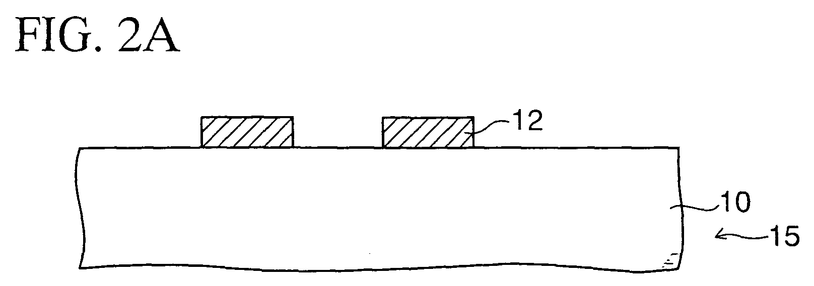
- FIGS.2A to 2D are sectional views showing an electroless plating method of a first embodiment of the present invention.
- a substrate 15 having a structure in which Cu electrodes 12 as an example of the conductive patterns are formed on an insulating body 10 is prepared.
- this substrate 15 is the wiring substrate on which electronic parts are packaged, and connection pads of the electronic parts are connected to the Cu electrodes 12 on the substrate 15.
- a Ni layer and a gold layer are formed on the Cu electrodes 12 by the electroless plating.
- the electroless plating method of an embodiment of the present invention can be applied to the step of forming selectively various metal layers on the conductive patterns.
- explanation is made with the step of forming the Ni layer on the Cu electrodes 12 taken as an example.
- the substrate 15 is cleaned with ethanol to degrease, and then is dipped into a 50 % hydrochloric acid (HCl) solution to apply the soft etching to surfaces of the substrate 15. Then, the substrate 15 is dipped into a tin chloride (II)(SnCl 2 ) solution (sensitization solution) to adhere Sn (II) ions onto the substrate 15.
- HCl hydrochloric acid
- the substrate 15 is dipped into a palladium chloride (PdCl 2 ) solution (activation solution).
- PdCl 2 palladium chloride
- the oxidation-reduction reaction advances based on a following reaction formula (1) to reduce (activate) Pd (II) ions, and thus Pd 14 (catalytic metal) is deposited and adhered onto the Cu electrodes 12.
- the surfaces of the Cu electrodes 12 are covered with the Pd 14 to exhibit the strong catalytic action on the electroless plating.
- the Pd 14 is adhered slightly onto the insulating body 10. Therefore, as described above, the plating is slightly applied to the space portions S between the Cu electrodes 12, so that it is possible that the Cu electrodes 12 are electrically short-circuited mutually.
- a protection film 16 is formed selectively on the space portions S (e.g., portions of 30 ⁇ m or less) between the Cu electrodes 12 in the subsequent step.
- an insulating film such as a resist film, a polyimide film, or the like is employed.
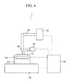
- FIG.4 is a schematic view showing an ink jet apparatus used in the present embodiment.
- an ink jet apparatus 1 according to the present embodiment has a stage 22 on which the substrate 15 is loaded. This stage 22 is connected to a stage moving means 26 for moving the stage 22. Accordingly, the stage 22 can be moved to any position in the horizontal direction containing X-Y directions.
- the substrate 15 is fixed onto the stage 22 by a chucking means (not shown) such as a vacuum chuck, or the like. Also, a heating means 24 such as a heater, or the like for heating the substrate 15 is provided to the stage 22, so that the substrate 15 can be heated.
- a chucking means such as a vacuum chuck, or the like.
- a heating means 24 such as a heater, or the like for heating the substrate 15 is provided to the stage 22, so that the substrate 15 can be heated.
- a coating means 28 containing a plurality of nozzles that spray a liquid 3 onto the substrate 15 to coat it is arranged over the stage 22.
- the coating means 28 is connected to a liquid supplying portion 32 via a piping 30.
- a nozzle controlling means 34 is connected to the coating means 28 to select the nozzle of the coating means 28 and control the spray characteristics, etc.
- the ink jet apparatus 1 has a controller 35.
- This controller 35 is connected to the stage moving means 26, the heating means 24, the liquid supplying portion 32, and the nozzle controlling means 34.
- the controller 35 controls the position of the substrate 15 on which the liquid 3 is coated, the spray characteristics of the liquid 3 from the coating means 28, etc.
- the bubble jet system in which the liquid is sprayed from the nozzle by generating the bubble in the liquid filled in the nozzle by virtue of a heat generating body, or the piezo driving system in which the liquid is sprayed from the nozzle by using the piezo element is employed.
- the substrate 15 to which the above catalytic process is applied is loaded on the stage 22 of such ink jet apparatus 1. Then, the substrate 15 is fixed by the chucking means. Then, as shown in FIG.2C, while moving the stage 22 in the horizontal direction or in a state that the stage 22 is fixed, a coating liquid 3a such as resist, polyimide, or the like is coated selectively on the space portions S between the Cu electrodes 12 on the substrate 15 by the coating means 28 to form a coating film. Then, a resin film is formed by heating the coating film by means of the heating means 24 to obtain the protection film 16.
- a coating liquid 3a such as resist, polyimide, or the like
- the protection film 16 can be formed on the space portions S between the Cu electrodes 12 in a short time by using such ink jet apparatus 1 without the photolithography.
- the electroless plating solution is prepared to form the Ni layer by the electroless plating.
- a solution in which sodium hypophosphite (NaH 2 PO 2 ) as a reducing agent, ammonium sulfate ((NH 4 ) 2 SO 4 ) as a buffer agent, sodium citrate (C 3 H 4 (OH) (CO 2 Na) 3 ) as a complexing agent, and nickel sulfate (NiSO 4 ) as a metallic salt are mixed is employed.
- a Ni layer 18 (metal layer) is formed selectively on the Cu electrodes 12 by dipping the substrate 15, which is subjected to the catalytic process, in the above electroless plating solution. At this time, Ni is deposited based on a reaction formula (2) and thus the Ni layer 18 is formed. Ni 2 + +H 2 PO 2 - +3OH - ⁇ Ni+HPO 3 2- +2H 2 O
- the protection film 16 is coated on the space portions S between the Cu electrodes 12 at this time, the Pd 14 as the catalyst of the electroless plating is not exposed. Therefore, the Ni plating is not applied to the space portions S between the Cu electrodes 12.
- Ni particles 18a are plated on the insulating body 10 on which the protection film 16 is not formed.
- the Cu electrodes 12 are not electrically short-circuited mutually because the space portions between the Cu electrodes 12 are wide.
- the Ni layer 18 and a gold layer 20 are formed selectively on the Cu electrodes 12 on the substrate 15 by dipping the substrate 15 into the electroless plating solution for gold.
- an oxidizing agent having a function of oxidizing the deposited Pd 14 conversely may be coated on the space portions S between the Cu electrodes 12 by the ink jet apparatus 1. Accordingly, the Pd 14 deposited by reducing (activating) the Pd ions is oxidized conversely to become its inactive state.
- the Pd 14 in the portions on which the oxidizing agent is coated does not exhibit the catalytic action on the electroless plating. Therefore, the oxidation-reduction reaction based on the above reaction formula (2) is suppressed, and thus the Ni plating is not applied to the space portions S between the Cu electrodes 12.
- oxidizing agent for example, H 2 SO 4 or a mixed solution consisting of H 2 SO 4 and HCl, or the like is employed.
- such a mode is exemplified that the protection film 16 is not coated on the portions in which widths of the space portions S between the Cu electrodes 12 are set wide (portions in which the Cu electrodes 12 are not electrically short-circuited mutually even when the Ni particles are formed).
- the protection film 16 may be formed on the overall insulating body 10 on the portions except the Cu electrodes 12. In this case, since the plating is applied selectively only onto the Cu electrodes 12 to form the Ni layer 18, production yield of the products can be improved further.
- the Pd 14 as the catalyst of the electroless plating is adhered onto the insulating body 10 and the Cu electrodes 12, and then the protection film 16 is formed on the space portions S between the Cu electrodes 12 (or the oxidizing agent is coated). Then, the Ni layer 18 is formed selectively on the Cu electrodes 12 by the electroless plating.
- the Ni plating is not applied to the space portions S between the Cu electrodes 12, the Ni layer 18 can be formed selectively on the Cu electrodes 12 formed at a narrow pitch with good yield.
- the metal film can be formed on such conductive patterns by the electroless plating as a simple method with good yield.
- a mode is exemplified in which the technical idea of the present invention is applied to the step of electroless-plating the Ni layer 18 on the Cu electrodes 12.
- an embodiment of the present invention can be applied to the electroless plating step for various metals such as copper, gold, silver, cobalt, tin, palladium, etc., which are formed on the conductive patterns by the electroless plating using the catalytic action of the catalytic metal.
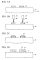
- FIGS.3A to 3D are sectional views showing an electroless plating method of a second embodiment of the present invention.
- a difference of the second embodiment from the first embodiment is that Pd is adhered selectively to Cu electrodes only. Detailed explanation of the similar steps to those in the first embodiment will be omitted herein.
- the substrate 15 having the structure in which the Cu electrodes 12 are formed on the insulating body 10 is prepared. Then, the substrate 15 is cleaned with ethanol, and then is dipped into the 50 % hydrochloric acid (HCl) solution to apply the soft etching to surfaces of the substrate 15. Then, the substrate 15 is dipped into the tin chloride (II) (SnCl 2 ) solution to adhere the Sn (II) ions onto the substrate 15.
- HCl hydrochloric acid
- the coating liquid 3a formed of the palladium chloride (PdCl 2 ) solution is coated selectively on the Cu electrodes 12 by the foregoing ink jet apparatus 1.
- the Pd 14 is deposited/adhered onto the surface of the Cu electrodes 12 by the oxidation-reduction reaction, which exhibits the strong catalytic action on the electroless plating.
- the Pd 14 is deposited based on the reaction formula (1) explained in the first embodiment.
- the Pd 14 is deposited selectively and adhered only onto the Cu electrodes 12. Therefore, since the Pd 14 does not exist on the insulating body 10 in portions except the Cu electrodes 12, such portions do not exhibit the catalytic action on the electroless plating.
- the substrate 15 is dipped into the electroless plating solution to form the Ni layer by the similar method to the first embodiment.
- the Ni layer 18 is formed selectively on the Cu electrodes 12.
- the Pd 14 is not adhered onto the insulating body 10 in the portions except the Cu electrodes 12, the Ni plating is not applied to the insulating body 10 and thus the Ni layer 18 is formed selectively on the Cu electrodes 12.
- the Au layer 20 is formed selectively on the Ni layer 18 by the electroless plating.
- the Cu electrodes 12 are by no means electrically short-circuited mutually, and therefore the Ni layer 18 and the Au layer 20 can be formed on the Cu electrodes 12 with good yield.
- the present invention can also be applied to the electroless plating method for various metals, which is used to form selectively the metal film by adhering the catalytic metal on the conductive patterns.
- the second embodiment can achieve the similar advantages to the first embodiment, and also can reduce a production cost rather than the first embodiment because the step of forming the protection film 16 is not required.
- the catalytic metal serving as the catalyst of the electroless plating is adhered onto the insulating body and the conductive patterns, and then the protection film or the oxidizing agent is formed selectively on the catalytic metal in the space portions between the conductive patterns. Then, the metal layer is formed selectively on the conductive patterns by the electroless plating.
- the catalytic metal is not exposed or the catalytic metal becomes inactive, in the space portions between the conductive patterns. Therefore, the electroless plating is not applied to the space portions between the conductive patterns. As a result, generation of the mutual electrical short-circuit between the patterns can be prevented even in the fine conductive patterns.
Landscapes
- Chemical & Material Sciences (AREA)
- Engineering & Computer Science (AREA)
- Metallurgy (AREA)
- Chemical Kinetics & Catalysis (AREA)
- Materials Engineering (AREA)
- Mechanical Engineering (AREA)
- General Chemical & Material Sciences (AREA)
- Organic Chemistry (AREA)
- Manufacturing & Machinery (AREA)
- Microelectronics & Electronic Packaging (AREA)
- Chemically Coating (AREA)
- Manufacturing Of Printed Wiring (AREA)
- Non-Metallic Protective Coatings For Printed Circuits (AREA)
Abstract
Description
Claims (8)
- An electroless plating method comprising the steps of:preparing a substrate (15) having an insulating body (10) and a conductive pattern (12) formed on the insulating body (10);adhering a catalytic metal (14) serving as a catalyst of an electroless plating onto the insulating body (10) and the conductive pattern (12);forming selectively a protection film (16), or an oxidizing agent used to oxidize the catalytic metal on the catalytic metal (14) in a space portion S between the conductive pattern (12); andforming selectively a metal layer (18) on the conductive pattern (12) by the electroless plating.
- An electroless plating method comprising the steps of:preparing a substrate (15) having an insulating body (10) and a conductive pattern (12) formed on the insulating body (10);adhering selectively a catalytic metal (14) serving as a catalyst of an electroless plating onto the conductive pattern (12); andforming selectively a metal layer (18) on the conductive pattern (12) by the electroless plating.
- An electroless plating method according to claim 1, wherein the step of forming selectively the protection film (16) or the oxidizing agent is carried out by an ink jet method.
- An electroless plating method according to claim 1, wherein the step of adhering the catalytic metal (14) onto the insulating body (10) and the conductive pattern (12) includes the step of coating an activating solution containing ions of the catalytic metal (14) to deposit the catalytic metal (14) by an oxidation-reduction reaction.
- An electroless plating method according to claim 1, 3 or 4, wherein the conductive pattern (12) is arranged in a state that the space portion between the conductive patterns has a plurality of different dimensions, and the protection film (16) or the oxidizing agent is formed selectively in portions, which are smaller than a predetermined dimension, out of the space portion between the conductive patterns (12).
- An electroless plating method according to claim 2, wherein the step of adhering selectively the catalytic metal (14) onto the conductive pattern (12) includes the step of coating selectively an activating solution containing ions of the catalytic metal (14) on the conductive pattern (12) by an ink jet method to deposit selectively the catalytic metal (14) on the conductive pattern (12) by an oxidation-reduction reaction.
- An electroless plating method according to any one of claims 1, 3, 4 or 5, wherein the protection film (16) is a resist film or a polyimide film.
- An electroless plating method according to any preceding claim, wherein the catalytic metal (14) is palladium, and the metal layer (18) formed by the electroless plating is a nickel layer or a copper layer.
Applications Claiming Priority (2)
| Application Number | Priority Date | Filing Date | Title |
|---|---|---|---|
| JP2003117828 | 2003-04-23 | ||
| JP2003117828A JP4198514B2 (en) | 2003-04-23 | 2003-04-23 | Electroless plating method |
Publications (2)
| Publication Number | Publication Date |
|---|---|
| EP1471167A2 true EP1471167A2 (en) | 2004-10-27 |
| EP1471167A3 EP1471167A3 (en) | 2005-02-02 |
Family
ID=32959619
Family Applications (1)
| Application Number | Title | Priority Date | Filing Date |
|---|---|---|---|
| EP04252270A Withdrawn EP1471167A3 (en) | 2003-04-23 | 2004-04-16 | Electroless plating method |
Country Status (3)
| Country | Link |
|---|---|
| US (1) | US20040213912A1 (en) |
| EP (1) | EP1471167A3 (en) |
| JP (1) | JP4198514B2 (en) |
Cited By (1)
| Publication number | Priority date | Publication date | Assignee | Title |
|---|---|---|---|---|
| WO2013083667A3 (en) * | 2011-12-07 | 2014-05-30 | Leopold Kostal Gmbh & Co. Kg | Method for producing an operating, decorative or display element that is galvanically coated on the front side and which has uncoated regions |
Families Citing this family (6)
| Publication number | Priority date | Publication date | Assignee | Title |
|---|---|---|---|---|
| US20050202583A1 (en) * | 2004-03-15 | 2005-09-15 | Canon Kabushiki Kaisha | Antistatic film forming composition, and producing method for conductive film pattern, electron source and image display apparatus |
| JP4680824B2 (en) * | 2006-04-21 | 2011-05-11 | 日立マクセル株式会社 | Method for forming plated film of polymer substrate and polymer substrate |
| TWI288590B (en) | 2005-10-31 | 2007-10-11 | Unimicron Technology Corp | Method of forming solder mask and circuit board with solder mask |
| KR101371088B1 (en) * | 2012-07-26 | 2014-03-12 | 한국과학기술연구원 | a fabricating method of metal thin film using electroless deposition and a thin film device fabricated thereby |
| US10465295B2 (en) * | 2014-05-20 | 2019-11-05 | Alpha Assembly Solutions Inc. | Jettable inks for solar cell and semiconductor fabrication |
| CN114481100B (en) * | 2022-04-01 | 2022-07-19 | 绍兴中芯集成电路制造股份有限公司 | Method for chemically plating metals with different thicknesses and packaging method of device |
Family Cites Families (19)
| Publication number | Priority date | Publication date | Assignee | Title |
|---|---|---|---|---|
| US3443988A (en) * | 1965-05-06 | 1969-05-13 | Photocircuits Corp | Printed circuits,work holders and method of preventing electroless metal deposition |
| US3573973A (en) * | 1967-11-13 | 1971-04-06 | Ibm | High speed additive circuit process |
| US3865623A (en) * | 1973-02-02 | 1975-02-11 | Litton Systems Inc | Fully additive process for manufacturing printed circuit boards |
| US4448804A (en) * | 1983-10-11 | 1984-05-15 | International Business Machines Corporation | Method for selective electroless plating of copper onto a non-conductive substrate surface |
| US4668533A (en) * | 1985-05-10 | 1987-05-26 | E. I. Du Pont De Nemours And Company | Ink jet printing of printed circuit boards |
| US4770899A (en) * | 1987-06-10 | 1988-09-13 | Unisys Corporation | Method of coating copper conductors on polyimide with a corrosion resistant metal, and module produced thereby |
| US4927462A (en) * | 1988-12-23 | 1990-05-22 | Associated Universities, Inc. | Oxidation of carbon fiber surfaces for use as reinforcement in high-temperature cementitious material systems |
| US5167992A (en) * | 1991-03-11 | 1992-12-01 | Microelectronics And Computer Technology Corporation | Selective electroless plating process for metal conductors |
| US5306389A (en) * | 1991-09-04 | 1994-04-26 | Osram Sylvania Inc. | Method of protecting aluminum nitride circuit substrates during electroless plating using a surface oxidation treatment |
| JPH05218020A (en) * | 1992-01-31 | 1993-08-27 | Nec Corp | Method of forming thin film wiring |
| JPH08199367A (en) * | 1995-01-20 | 1996-08-06 | Kenseidou Kagaku Kogyo Kk | Formation of contact metallic layer on optional surface part of resin molded good |
| US5549808A (en) * | 1995-05-12 | 1996-08-27 | International Business Machines Corporation | Method for forming capped copper electrical interconnects |
| JPH1070371A (en) * | 1996-08-26 | 1998-03-10 | Tokyo Ohka Kogyo Co Ltd | Manufacture of multilayer wiring board |
| WO1999018255A1 (en) * | 1997-10-03 | 1999-04-15 | Massachusetts Institute Of Technology | Selective substrate metallization |
| JP3614707B2 (en) * | 1999-04-28 | 2005-01-26 | 住友大阪セメント株式会社 | Method for producing translucent conductive film and translucent conductive film |
| JP2001251039A (en) * | 2000-03-07 | 2001-09-14 | Seiko Epson Corp | Glass substrate, method of manufacturing the same, and semiconductor device |
| JP2001335952A (en) * | 2000-05-31 | 2001-12-07 | Rikogaku Shinkokai | Electroless plating method, wiring device and its production method |
| US6754551B1 (en) * | 2000-06-29 | 2004-06-22 | Printar Ltd. | Jet print apparatus and method for printed circuit board manufacturing |
| JP2002026491A (en) * | 2000-07-06 | 2002-01-25 | Seiko Epson Corp | Printed circuit board plating method, mounting structure, liquid crystal device, and method of manufacturing liquid crystal device |
-
2003
- 2003-04-23 JP JP2003117828A patent/JP4198514B2/en not_active Expired - Fee Related
-
2004
- 2004-04-15 US US10/709,138 patent/US20040213912A1/en not_active Abandoned
- 2004-04-16 EP EP04252270A patent/EP1471167A3/en not_active Withdrawn
Cited By (1)
| Publication number | Priority date | Publication date | Assignee | Title |
|---|---|---|---|---|
| WO2013083667A3 (en) * | 2011-12-07 | 2014-05-30 | Leopold Kostal Gmbh & Co. Kg | Method for producing an operating, decorative or display element that is galvanically coated on the front side and which has uncoated regions |
Also Published As
| Publication number | Publication date |
|---|---|
| JP2004323885A (en) | 2004-11-18 |
| JP4198514B2 (en) | 2008-12-17 |
| EP1471167A3 (en) | 2005-02-02 |
| US20040213912A1 (en) | 2004-10-28 |
Similar Documents
| Publication | Publication Date | Title |
|---|---|---|
| EP0475567B1 (en) | Method for fabricating printed circuits | |
| US5380560A (en) | Palladium sulfate solution for the selective seeding of the metal interconnections on polyimide dielectrics for electroless metal deposition | |
| CN101668880B (en) | Connecting terminal, semiconductor package using connecting terminal and method for manufacturing semiconductor package | |
| US6261637B1 (en) | Use of palladium immersion deposition to selectively initiate electroless plating on Ti and W alloys for wafer fabrication | |
| US20110051387A1 (en) | Method for electroless nickel-palladium-gold plating, plated product, printed wiring board, interposer and semiconductor apparatus | |
| JP2008508703A (en) | Method for manufacturing an electronic circuit assembly | |
| EP1863327A1 (en) | Process for producing wiring board, and wiring board | |
| JPS6325518B2 (en) | ||
| US5167992A (en) | Selective electroless plating process for metal conductors | |
| US20040213912A1 (en) | Electroless plating method | |
| JP2001519477A (en) | Methods and solutions for producing a gold layer | |
| JP2005029735A (en) | Method for forming polyimide resin inorganic thin film and surface modified polyimide resin for forming inorganic thin film | |
| JP2003160876A (en) | Catalyst for electroless plating and method for forming metal plating pattern | |
| KR20060064549A (en) | Inorganic thin film formation method of polyimide resin and manufacturing method of polyimide resin for surface modified inorganic thin film formation | |
| KR20070118073A (en) | Method of depositing palladium layers and palladium bath for the same | |
| WO2004056162A1 (en) | Flip-chip mounting electronic component and method for producing the same, circuit board and method for producing the same, method for producing package | |
| US5855959A (en) | Process for providing catalytically active platinum metal layers | |
| CN100428871C (en) | Method for forming metal wire pattern by ink-jet method | |
| US6773760B1 (en) | Method for metallizing surfaces of substrates | |
| JPH0669632A (en) | Manufacture of printed wiring board | |
| KR20060006536A (en) | Plating layer formation method of printed circuit board for semiconductor package and printed circuit board manufactured therefrom | |
| JP2003293143A (en) | Cleaning agent for palladium catalyst, method for cleaning palladium catalyst, method for plating electronic parts using the agent, and electronic parts | |
| JPH0480374A (en) | Production of printed circuit board | |
| JP2006188757A (en) | Method for forming polyimide resin inorganic thin film and surface modified polyimide resin for forming inorganic thin film | |
| US20220064801A1 (en) | Method for electroless nickel deposition onto copper without activation with palladium |
Legal Events
| Date | Code | Title | Description |
|---|---|---|---|
| PUAI | Public reference made under article 153(3) epc to a published international application that has entered the european phase |
Free format text: ORIGINAL CODE: 0009012 |
|
| AK | Designated contracting states |
Kind code of ref document: A2 Designated state(s): AT BE BG CH CY CZ DE DK EE ES FI FR GB GR HU IE IT LI LU MC NL PL PT RO SE SI SK TR |
|
| AX | Request for extension of the european patent |
Extension state: AL HR LT LV MK |
|
| PUAL | Search report despatched |
Free format text: ORIGINAL CODE: 0009013 |
|
| AK | Designated contracting states |
Kind code of ref document: A3 Designated state(s): AT BE BG CH CY CZ DE DK EE ES FI FR GB GR HU IE IT LI LU MC NL PL PT RO SE SI SK TR |
|
| AX | Request for extension of the european patent |
Extension state: AL HR LT LV MK |
|
| 17P | Request for examination filed |
Effective date: 20050427 |
|
| AKX | Designation fees paid |
Designated state(s): DE GB |
|
| 17Q | First examination report despatched |
Effective date: 20070319 |
|
| STAA | Information on the status of an ep patent application or granted ep patent |
Free format text: STATUS: THE APPLICATION IS DEEMED TO BE WITHDRAWN |
|
| 18D | Application deemed to be withdrawn |
Effective date: 20110607 |