EP1469558B1 - Connector adapted to be used for transmission of a balanced signal and substrate for mounting the connector - Google Patents
Connector adapted to be used for transmission of a balanced signal and substrate for mounting the connector Download PDFInfo
- Publication number
- EP1469558B1 EP1469558B1 EP04009025A EP04009025A EP1469558B1 EP 1469558 B1 EP1469558 B1 EP 1469558B1 EP 04009025 A EP04009025 A EP 04009025A EP 04009025 A EP04009025 A EP 04009025A EP 1469558 B1 EP1469558 B1 EP 1469558B1
- Authority
- EP
- European Patent Office
- Prior art keywords
- signal
- contact
- intermediate portion
- connector
- signal contact
- Prior art date
- Legal status (The legal status is an assumption and is not a legal conclusion. Google has not performed a legal analysis and makes no representation as to the accuracy of the status listed.)
- Expired - Fee Related
Links
Images


Classifications
-
- H—ELECTRICITY
- H01—ELECTRIC ELEMENTS
- H01R—ELECTRICALLY-CONDUCTIVE CONNECTIONS; STRUCTURAL ASSOCIATIONS OF A PLURALITY OF MUTUALLY-INSULATED ELECTRICAL CONNECTING ELEMENTS; COUPLING DEVICES; CURRENT COLLECTORS
- H01R13/00—Details of coupling devices of the kinds covered by groups H01R12/70 or H01R24/00 - H01R33/00
- H01R13/646—Details of coupling devices of the kinds covered by groups H01R12/70 or H01R24/00 - H01R33/00 specially adapted for high-frequency, e.g. structures providing an impedance match or phase match
- H01R13/6461—Means for preventing cross-talk
- H01R13/6471—Means for preventing cross-talk by special arrangement of ground and signal conductors, e.g. GSGS [Ground-Signal-Ground-Signal]
-
- H—ELECTRICITY
- H01—ELECTRIC ELEMENTS
- H01R—ELECTRICALLY-CONDUCTIVE CONNECTIONS; STRUCTURAL ASSOCIATIONS OF A PLURALITY OF MUTUALLY-INSULATED ELECTRICAL CONNECTING ELEMENTS; COUPLING DEVICES; CURRENT COLLECTORS
- H01R13/00—Details of coupling devices of the kinds covered by groups H01R12/70 or H01R24/00 - H01R33/00
- H01R13/646—Details of coupling devices of the kinds covered by groups H01R12/70 or H01R24/00 - H01R33/00 specially adapted for high-frequency, e.g. structures providing an impedance match or phase match
- H01R13/6473—Impedance matching
- H01R13/6474—Impedance matching by variation of conductive properties, e.g. by dimension variations
-
- H—ELECTRICITY
- H01—ELECTRIC ELEMENTS
- H01R—ELECTRICALLY-CONDUCTIVE CONNECTIONS; STRUCTURAL ASSOCIATIONS OF A PLURALITY OF MUTUALLY-INSULATED ELECTRICAL CONNECTING ELEMENTS; COUPLING DEVICES; CURRENT COLLECTORS
- H01R13/00—Details of coupling devices of the kinds covered by groups H01R12/70 or H01R24/00 - H01R33/00
- H01R13/648—Protective earth or shield arrangements on coupling devices, e.g. anti-static shielding
- H01R13/658—High frequency shielding arrangements, e.g. against EMI [Electro-Magnetic Interference] or EMP [Electro-Magnetic Pulse]
- H01R13/6581—Shield structure
- H01R13/6585—Shielding material individually surrounding or interposed between mutually spaced contacts
- H01R13/6589—Shielding material individually surrounding or interposed between mutually spaced contacts with wires separated by conductive housing parts
-
- H—ELECTRICITY
- H01—ELECTRIC ELEMENTS
- H01R—ELECTRICALLY-CONDUCTIVE CONNECTIONS; STRUCTURAL ASSOCIATIONS OF A PLURALITY OF MUTUALLY-INSULATED ELECTRICAL CONNECTING ELEMENTS; COUPLING DEVICES; CURRENT COLLECTORS
- H01R13/00—Details of coupling devices of the kinds covered by groups H01R12/70 or H01R24/00 - H01R33/00
- H01R13/648—Protective earth or shield arrangements on coupling devices, e.g. anti-static shielding
- H01R13/658—High frequency shielding arrangements, e.g. against EMI [Electro-Magnetic Interference] or EMP [Electro-Magnetic Pulse]
- H01R13/6591—Specific features or arrangements of connection of shield to conductive members
- H01R13/6594—Specific features or arrangements of connection of shield to conductive members the shield being mounted on a PCB and connected to conductive members
- H01R13/6595—Specific features or arrangements of connection of shield to conductive members the shield being mounted on a PCB and connected to conductive members with separate members fixing the shield to the PCB
Description
- This application claims priority to prior Japanese application JP 2003-111567.
- This invention relates to a connector suitable for connection of a transmission line or an electric line for transmitting a balanced signal and a substrate for mounting the connector.
- A connector of the type is disclosed, for example, in Japanese Patent (JP-B) No. 3108239 and comprises an insulator and a plurality of pairs of signal contacts (signal contact pairs) held by the insulator. Each of the signal contact pairs are connected to a pair of transmission lines for transmitting a balanced signal.
- Each of the signal contacts is formed primarily by press punching. In this case, each signal contact tends to be partially varied in sectional shape. It is therefore difficult to achieve impedance matching between the signal contacts in each of the signal contact pairs.
- In case where the adjustment of impedance is essential and indispensable, it is inevitable to change the shape in punching. The change in shape in punching requires a high cost.
- From JP-243936A a connector to mount on a substrate can be taken which is suitable for a connection of a transmission line or an electric line for transmitting a balance signal. The connector comprises signal contacts.
- Each signal contact comprises a fixed portion fixed to the insulator; a contacting portion connected to one end of the fixed portion and extending in a first direction; a first intermediate portion extending in the first direction; a second intermediate portion extending from the first intermediate portion extending in a second direction perpendicular to the first direction; a terminal portion extending from the second intermediate portion in the first direction; wherein the first intermediate portion of each signal contact is placed at positions being different from each other in the second direction; and wherein the second intermediate portion of each signal contact is placed in positions being different from each other in the first direction.
- It is therefore an object of the present invention to provide a connector which has an excellent impedance characteristic and which is suitable for transmission of a balanced signal.
- It is another object of the present invention to provide a connector which is capable of preventing occurrence of crosstalk between adjacent ones of the above-mentioned signal contact pairs.
- It is still another object of the present invention to provide a combination of a substrate and the above-mentioned connector and which is prevented from degradation in impedance characteristic.
- Other objects of the present invention will become clear as the description proceeds.
- According to one aspect of the present invention, there is provided a connector as claimed in the independent claim 1.
- According to another aspect of the present invention, there is provided a combination of a substrate and the connector according to one of claims 1 to 8.
-
- Fig. 1 is a perspective view of a connector according to one embodiment of the present invention, together with a substrate for mounting the connector;
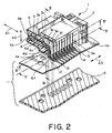
- Fig. 2 is a perspective view of the connector illustrated in Fig. 1 with a part cut away along a line II-II, together with the substrate divided into two parts in a thickness direction for convenience of description;
- Fig. 3 is a sectional view of a characteristic part of a contact portion, taken along a line III-III in Fig. 2;
- Fig. 4 is a sectional view of a characteristic part of the connector, taken along a line IV-IV in Fig. 2;
- Fig. 5 is a sectional view of a characteristic part, taken along a line V-V in Fig. 2, and shows the relationship between the contact portion and the substrate,;
- Fig. 6 is an enlarged sectional view taken along a line VI-VI in Fig. 1; and
- Fig. 7 is an enlarged sectional view taken along a line VII-VII in Fig. 1.
- Referring to Figs. 1 and 2, description will be made of a connector according to one embodiment of the present invention.
- The connector depicted by 1 in the figure is a so-called angle connector and is coupled and connected to a mating connector (not shown) in a first direction A1 in order to connect a transmission line for transmitting a balanced signal. The connector 1 is mounted to a substrate 11, such as a printed board, in a second direction A2 perpendicular to the first direction A1. A direction perpendicular to the first and the second directions A1 and A2 will be called a third direction A3.
- The connector 1 comprises an
insulator 2 and a number of pairs of conductive signal contacts (signal contact pairs) 3 and 4 held by theinsulator 2. The signal contact pairs are arranged in parallel to one another at a predetermined pitch in the third direction A3. On opposite sides of every signal contact pair in the third direction A3,conductive ground contacts 5 are disposed adjacent to and spaced from the signal contact pair. Each of theground contacts 5 extends in the first and the second directions A1 and A2 in a plate-like shape. Eachground contact 5 has aflat plate portion 5a press-fitted and fixed to theinsulator 2 and aterminal portion 5b protruding from theflat plate portion 5a. Theground contacts 5 serve to prevent occurrence of crosstalk between the signal contact pairs. Theinsulator 2 has a coupling portion covered with ashell 6 on upper and lower sides thereof. - In the following description, one of the signal contacts in each pair will be called a
first signal contact 3 and the other will be called asecond signal contact 4. Each of the first and thesecond signal contacts insulator 2, thefirst signal contact 3 is disposed at a position higher than that of thesecond signal contact 4 as a whole. The first and the second signal contacts 3 and 4 form an electric pair upon transmission of the balanced signal. - The
first signal contact 3 has a fixed portion 3a press-fitted and fixed to theinsulator 2, a contactingportion 3b having elasticity, connected to one end of the fixed portion 3a, and extending forward in the first direction A1, i.e., in a coupling direction, abent portion 3c connected to the other end of the fixed portion 3a, a firstintermediate portion 3d extending from thebent portion 3c rearward in the first direction A1, a secondintermediate portion 3e extending from a rear end of the firstintermediate portion 3d downward in the second direction A2, and aterminal portion 3f extending from a lower end of the secondintermediate portion 3e rearward in the first direction A1 to be soldered to a substrate 11. - On the other hand, the
second signal contact 4 has a fixed portion 4a press-fitted and fixed to theinsulator 2, a contacting portion 4b having elasticity, connected to one end of the fixed portion 4a, and extending forward in the first direction A1, i.e., in the coupling direction, abent portion 4c connected to the other end of the fixed portion 4a, a firstintermediate portion 4d extending from thebent portion 4c rearward in the first direction A1, a secondintermediate portion 4e extending from a rear end of the firstintermediate portion 4d downward in the second direction A2, and aterminal portion 4f extending from a lower end of the secondintermediate portion 4e rearward in the first direction A1 to be soldered to the substrate 11. - The contacting portion 3a of the
first signal contact 3 and the contacting portion 4a of thesecond signal contact 4 are faced to each other with a space left therebetween in the second direction A2. The contacting portions 3a and 4a form a socket. Between the contacting portions 3a and 4a, a pin contact of the mating connector is inserted in contact therewith. - As is obvious from Fig. 3, the first
intermediate portion 3d of thefirst signal contact 3 and the firstintermediate portion 4d of thesecond signal contact 4 are displaced or shifted in position from each other in the second direction A2 by a distance X1 and also displaced or shifted in position from each other in the third direction A3. In other words, the firstintermediate portions - As is obvious from Fig. 4, the second
intermediate portion 3e of thefirst signal contact 3 and the secondintermediate portion 4e of thesecond signal contact 4 are displaced or shifted in position from each other in the first direction A1 by a distance X2 and also displaced or shifted in position from each other in the third direction A3. In other words, the secondintermediate portions - As is obvious from Fig. 5, the
terminal portion 3f of thefirst signal contact 3 and theterminal portion 4f of thesecond signal contact 4 are disposed adjacent to each other in the third direction A3. - The
bent portion 3c of the first signal contact 3 and thebent portion 4c of thesecond signal contact 4 cooperate with each other to make the first and thesecond signal contacts bent portions second signal contacts second signal contacts - Next referring to Figs. 6 and 7 in addition to Figs. 1 and 2, the substrate 11 will be described.
- The substrate 11 has a multilayer micro strip line structure. The substrate 11 has a surface 11 a provided with a number of
signal pads 12 corresponding to theterminal portions second signal contacts ground pads 13 connected to thesignal pads 12, and a number ofground pads 14 corresponding to theground contacts 5. Inside the substrate 11, a ground layer 1t extends in parallel to the surface 11 a. - In Fig. 2, the substrate 11 is divided into two parts in a thickness direction. The
ground layer 15 is formed in a hatched region in the figure. Thus, theground layer 15 extends over an area except at least those portions faced to thesignal pads 12 in the second direction A2. In other words, theground layer 15 is locally removed at the portions located below thesignal pads 12. With the above-mentioned structure, it is possible to suppress the decrease in impedance without increasing occurrence of crosstalk between the signal contact pairs. - As shown in Fig. 5, the
terminal portions signal contacts signal pads 12 of the substrate 11 by SMT (surface mount technology), respectively. Theterminal portions 5b of theground contacts 5 are soldered to theground pads 13, respectively. - While the present invention has thus far been described in conjunction with the preferred embodiment thereof, it will be readily possible for those skilled in the art to put this invention into practice in various other manners without departing from the scope set forth in the appended claims. For example, press punching may form each of the signal contacts.
Claims (9)
- A connector (1) comprising an insulator (2) and first and second signal contacts (3, 4) held by the insulator (2), each of the first and the second signal contacts (3, 4) comprising:a fixed portion (3a, 4a) fixed to the insulator (2), a contacting portion (3b, 4b) connected to one end of the fixed portion (3a, 4a) and extending in a first direction (A1);a bent portion (3c, 4c) connected to the other end of the fixed portion (3a, 4a);a first intermediate portion (3d, 4d) extending from the bent portion (3c, 4c) in the first direction (A1);a second intermediate portion (3e, 4e) extending from the first intermediate portion (3d, 4d) in a second direction (A2) perpendicular to the first direction (A1); anda terminal portion (3f, 4f) extending from the second intermediate portion (3e, 4e) in the first direction (A1), the first intermediate portion (3d) of the first signal contact (3) and the first intermediate portion (4d) of the second signal contact (4) being placed at positions which are different from each other in the second direction (A2), the second intermediate portion (3e) of the first signal contact (3) and the second intermediate portion (4e) of the second signal contact (4) being different from each other in the first direction (A1), the bent portions (3c, 4c) being shaped to make the first and the second signal contacts (3, 4) be substantially equal in total length to each other.
- The connector according to claim 1, wherein the first intermediate portion (3d) of the first signal contact (3) and the first intermediate portion (4d) of the second signal contact (4) are placed at positions which are different from each other in a third direction (A3) perpendicular to the first and the second direction (A1, A2).
- The connector according to claim 1 or 2, wherein the second intermediate portion (3e) of the first signal contact (3)and the second intermediate portion (4e) of the second signal contact (4) are placed at positions which are different from each other in a third direction (A3) perpendicular to the first and the second directions (A1, A2).
- The connector according to one of claims 1 to 3, wherein the contacting portion (3b) of the first signal contact (3) and the contacting portion (4b) of the second signal contact (4) are faced to each other in the second directions (A2).
- The connector according to one of claims 1 to 4, wherein the terminal portion (3f) of the first signal contact (3) and the terminal portion (4f) of the second signal contact (4) are disposed adjacent to each other in a third direction (A3) perpendicular to the first and second directions (A1, A2).
- The connector according to one of claims 1 to 5, further comprising a first ground contact (5) held by the insulator (2), a combination of the first and the second signal contacts (3, 4) forming a contact pair, the first ground contact (5) being disposed adjacent to the contact pair on one side of the contact pair in a third direction (A3) perpendicular to the first and the second directions (A1, A2), preferably the first ground contact (5) extends in the first and the second directions (A1, A2) in a plate-like shape.
- The connector according to one of claims 1 to 6, comprising a second ground (5) contact held by the insulator (2) and disposed adjacent to the contact pair on the other side of the contact pair in the third direction, preferably the second ground contact (5) extends in the first and the second directions (A1, A2) in a plate-like shape.
- The connector according to one of claims 1 to 7, wherein the first and the second ground contacts (5) are used for transmission of a balanced signal.
- A combination of a substrate (11) and the connector (1) according to one of claims 1 to 8, the substrate (11) comprising:a plate portion; (12)first and second signal pads (12) disposed on a surface of the plate portion and adapted to be connected to the terminal portions (3f, 4f) of the first and the second signal contacts (3, 4); anda ground layer (15) formed inside the plate portion and extending in parallel to the surface (11a) of the plate portion over an area except at least those portions faced to the first and the second signal pads (12) in the second direction (A2).
Applications Claiming Priority (2)
| Application Number | Priority Date | Filing Date | Title |
|---|---|---|---|
| JP2003111567A JP2004319257A (en) | 2003-04-16 | 2003-04-16 | Balanced transmission connector |
| JP2003111567 | 2003-04-16 |
Publications (3)
| Publication Number | Publication Date |
|---|---|
| EP1469558A2 EP1469558A2 (en) | 2004-10-20 |
| EP1469558A3 EP1469558A3 (en) | 2004-12-29 |
| EP1469558B1 true EP1469558B1 (en) | 2006-09-06 |
Family
ID=32906038
Family Applications (1)
| Application Number | Title | Priority Date | Filing Date |
|---|---|---|---|
| EP04009025A Expired - Fee Related EP1469558B1 (en) | 2003-04-16 | 2004-04-15 | Connector adapted to be used for transmission of a balanced signal and substrate for mounting the connector |
Country Status (6)
| Country | Link |
|---|---|
| US (1) | US6974336B2 (en) |
| EP (1) | EP1469558B1 (en) |
| JP (1) | JP2004319257A (en) |
| CN (1) | CN1279661C (en) |
| DE (1) | DE602004002229T2 (en) |
| TW (1) | TWI276262B (en) |
Families Citing this family (5)
| Publication number | Priority date | Publication date | Assignee | Title |
|---|---|---|---|---|
| CN2932689Y (en) | 2006-04-10 | 2007-08-08 | 富士康(昆山)电脑接插件有限公司 | Electric connector |
| JP5054462B2 (en) * | 2007-08-06 | 2012-10-24 | 富士通コンポーネント株式会社 | Balanced transmission connector |
| JP4839362B2 (en) * | 2008-11-14 | 2011-12-21 | ホシデン株式会社 | High frequency circuit module |
| JP4887393B2 (en) * | 2009-03-24 | 2012-02-29 | ホシデン株式会社 | connector |
| JP6215125B2 (en) * | 2014-04-21 | 2017-10-18 | 日本航空電子工業株式会社 | connector |
Family Cites Families (12)
| Publication number | Priority date | Publication date | Assignee | Title |
|---|---|---|---|---|
| US5085601A (en) * | 1990-12-11 | 1992-02-04 | Amp Incorporated | Reduced insertion force electrical connector |
| US5244412A (en) * | 1991-12-24 | 1993-09-14 | Stewart Connector Systems, Inc. | Electrical device for surface mounting on a circuit board and mounting component thereof |
| JP3108239B2 (en) | 1993-02-19 | 2000-11-13 | 富士通株式会社 | Impedance matched electrical connector |
| JPH0785931A (en) * | 1993-09-17 | 1995-03-31 | Kel Corp | Connector |
| JP2715910B2 (en) | 1994-06-27 | 1998-02-18 | 日本電気株式会社 | Multilayer printed wiring board and method of manufacturing the same |
| JP3232225B2 (en) * | 1995-11-15 | 2001-11-26 | ヒロセ電機株式会社 | Information card, back connector and card blank therefor |
| US5795191A (en) * | 1996-09-11 | 1998-08-18 | Preputnick; George | Connector assembly with shielded modules and method of making same |
| US6503103B1 (en) * | 1997-02-07 | 2003-01-07 | Teradyne, Inc. | Differential signal electrical connectors |
| JP3238895B2 (en) * | 1997-08-28 | 2001-12-17 | ヒロセ電機株式会社 | Modular jack |
| US5919063A (en) * | 1997-09-17 | 1999-07-06 | Berg Technology, Inc. | Three row plug and receptacle connectors with ground shield |
| JP2000068006A (en) * | 1998-08-20 | 2000-03-03 | Fujitsu Takamisawa Component Ltd | Right-angle type connector |
| JP2000068007A (en) | 1998-08-20 | 2000-03-03 | Fujitsu Takamisawa Component Ltd | Connector for balanced transmission with cable |
-
2003
- 2003-04-16 JP JP2003111567A patent/JP2004319257A/en active Pending
-
2004
- 2004-03-30 CN CNB2004100318186A patent/CN1279661C/en not_active Expired - Fee Related
- 2004-04-13 US US10/823,025 patent/US6974336B2/en not_active Expired - Fee Related
- 2004-04-15 TW TW093110449A patent/TWI276262B/en not_active IP Right Cessation
- 2004-04-15 EP EP04009025A patent/EP1469558B1/en not_active Expired - Fee Related
- 2004-04-15 DE DE602004002229T patent/DE602004002229T2/en not_active Expired - Fee Related
Also Published As
| Publication number | Publication date |
|---|---|
| TWI276262B (en) | 2007-03-11 |
| JP2004319257A (en) | 2004-11-11 |
| US20040209496A1 (en) | 2004-10-21 |
| DE602004002229T2 (en) | 2007-07-19 |
| CN1538578A (en) | 2004-10-20 |
| TW200428718A (en) | 2004-12-16 |
| US6974336B2 (en) | 2005-12-13 |
| EP1469558A2 (en) | 2004-10-20 |
| EP1469558A3 (en) | 2004-12-29 |
| DE602004002229D1 (en) | 2006-10-19 |
| CN1279661C (en) | 2006-10-11 |
Similar Documents
| Publication | Publication Date | Title |
|---|---|---|
| US7172434B2 (en) | Electrical connection apparatus capable of resisting repetition of connection and disconnection | |
| US7310875B2 (en) | Connector for high-speed communications | |
| US7435110B2 (en) | Electrical connector with improved contact arrangement | |
| US6808419B1 (en) | Electrical connector having enhanced electrical performance | |
| CN100585953C (en) | Board-to-board connector | |
| US7549882B2 (en) | Connector capable of absorbing an error in mounting position | |
| US7604510B2 (en) | High speed transmission connector | |
| US6592407B2 (en) | High-speed card edge connector | |
| US20050042924A1 (en) | Electrical connector having shielding plates | |
| JPH0613134A (en) | Connector having grounding bus | |
| EP1453152B1 (en) | Connector in which occurrence of crosstalk is suppressed by a ground contact | |
| KR20010051954A (en) | Flexible connector integrally having transmission line | |
| CN101505025B (en) | Connector | |
| JP3762730B2 (en) | connector | |
| EP1469558B1 (en) | Connector adapted to be used for transmission of a balanced signal and substrate for mounting the connector | |
| US6817868B2 (en) | Intermediate board electrical connector | |
| US6663445B1 (en) | Electrical connector with staggered contacts | |
| US7004763B2 (en) | Board-to-board electrical connector assembly | |
| US7413475B2 (en) | Electrical connector having ground planes | |
| US7445470B2 (en) | Electrical connector with improved housing | |
| EP1063726A2 (en) | Electrical connector with multiple terminals | |
| CN210111110U (en) | Electrical connector | |
| US6979237B2 (en) | Electrical connector having receptacle contacts | |
| CN114927894A (en) | Electrical connector with improved contact arrangement | |
| CN115588885A (en) | High-speed transmission connector |
Legal Events
| Date | Code | Title | Description |
|---|---|---|---|
| PUAI | Public reference made under article 153(3) epc to a published international application that has entered the european phase |
Free format text: ORIGINAL CODE: 0009012 |
|
| AK | Designated contracting states |
Kind code of ref document: A2 Designated state(s): AT BE BG CH CY CZ DE DK EE ES FI FR GB GR HU IE IT LI LU MC NL PL PT RO SE SI SK TR |
|
| AX | Request for extension of the european patent |
Extension state: AL HR LT LV MK |
|
| 17P | Request for examination filed |
Effective date: 20040910 |
|
| PUAL | Search report despatched |
Free format text: ORIGINAL CODE: 0009013 |
|
| AK | Designated contracting states |
Kind code of ref document: A3 Designated state(s): AT BE BG CH CY CZ DE DK EE ES FI FR GB GR HU IE IT LI LU MC NL PL PT RO SE SI SK TR |
|
| AX | Request for extension of the european patent |
Extension state: AL HR LT LV MK |
|
| AKX | Designation fees paid |
Designated state(s): DE FR GB |
|
| GRAP | Despatch of communication of intention to grant a patent |
Free format text: ORIGINAL CODE: EPIDOSNIGR1 |
|
| GRAS | Grant fee paid |
Free format text: ORIGINAL CODE: EPIDOSNIGR3 |
|
| GRAA | (expected) grant |
Free format text: ORIGINAL CODE: 0009210 |
|
| AK | Designated contracting states |
Kind code of ref document: B1 Designated state(s): DE FR GB |
|
| REG | Reference to a national code |
Ref country code: GB Ref legal event code: FG4D |
|
| REF | Corresponds to: |
Ref document number: 602004002229 Country of ref document: DE Date of ref document: 20061019 Kind code of ref document: P |
|
| ET | Fr: translation filed | ||
| PLBE | No opposition filed within time limit |
Free format text: ORIGINAL CODE: 0009261 |
|
| STAA | Information on the status of an ep patent application or granted ep patent |
Free format text: STATUS: NO OPPOSITION FILED WITHIN TIME LIMIT |
|
| 26N | No opposition filed |
Effective date: 20070607 |
|
| PGFP | Annual fee paid to national office [announced via postgrant information from national office to epo] |
Ref country code: DE Payment date: 20080430 Year of fee payment: 5 |
|
| GBPC | Gb: european patent ceased through non-payment of renewal fee |
Effective date: 20080415 |
|
| PG25 | Lapsed in a contracting state [announced via postgrant information from national office to epo] |
Ref country code: GB Free format text: LAPSE BECAUSE OF NON-PAYMENT OF DUE FEES Effective date: 20080415 |
|
| REG | Reference to a national code |
Ref country code: FR Ref legal event code: ST Effective date: 20091231 |
|
| PG25 | Lapsed in a contracting state [announced via postgrant information from national office to epo] |
Ref country code: DE Free format text: LAPSE BECAUSE OF NON-PAYMENT OF DUE FEES Effective date: 20091103 |
|
| PG25 | Lapsed in a contracting state [announced via postgrant information from national office to epo] |
Ref country code: FR Free format text: LAPSE BECAUSE OF NON-PAYMENT OF DUE FEES Effective date: 20091222 |
|
| PGFP | Annual fee paid to national office [announced via postgrant information from national office to epo] |
Ref country code: FR Payment date: 20080428 Year of fee payment: 5 |