EP1469517A2 - Organic electro-luminescence display and manufacturing method threof - Google Patents
Organic electro-luminescence display and manufacturing method threof Download PDFInfo
- Publication number
- EP1469517A2 EP1469517A2 EP04008726A EP04008726A EP1469517A2 EP 1469517 A2 EP1469517 A2 EP 1469517A2 EP 04008726 A EP04008726 A EP 04008726A EP 04008726 A EP04008726 A EP 04008726A EP 1469517 A2 EP1469517 A2 EP 1469517A2
- Authority
- EP
- European Patent Office
- Prior art keywords
- organic
- bulkhead
- display panel
- supplement
- strip
- Prior art date
- Legal status (The legal status is an assumption and is not a legal conclusion. Google has not performed a legal analysis and makes no representation as to the accuracy of the status listed.)
- Withdrawn
Links
Images






Classifications
-
- H—ELECTRICITY
- H05—ELECTRIC TECHNIQUES NOT OTHERWISE PROVIDED FOR
- H05B—ELECTRIC HEATING; ELECTRIC LIGHT SOURCES NOT OTHERWISE PROVIDED FOR; CIRCUIT ARRANGEMENTS FOR ELECTRIC LIGHT SOURCES, IN GENERAL
- H05B33/00—Electroluminescent light sources
- H05B33/02—Details
- H05B33/04—Sealing arrangements, e.g. against humidity
-
- H—ELECTRICITY
- H10—SEMICONDUCTOR DEVICES; ELECTRIC SOLID-STATE DEVICES NOT OTHERWISE PROVIDED FOR
- H10K—ORGANIC ELECTRIC SOLID-STATE DEVICES
- H10K59/00—Integrated devices, or assemblies of multiple devices, comprising at least one organic light-emitting element covered by group H10K50/00
- H10K59/10—OLED displays
- H10K59/17—Passive-matrix OLED displays
- H10K59/179—Interconnections, e.g. wiring lines or terminals
- H10K59/1795—Interconnections, e.g. wiring lines or terminals comprising structures specially adapted for lowering the resistance
-
- H—ELECTRICITY
- H10—SEMICONDUCTOR DEVICES; ELECTRIC SOLID-STATE DEVICES NOT OTHERWISE PROVIDED FOR
- H10K—ORGANIC ELECTRIC SOLID-STATE DEVICES
- H10K50/00—Organic light-emitting devices
- H10K50/80—Constructional details
- H10K50/84—Passivation; Containers; Encapsulations
- H10K50/842—Containers
- H10K50/8426—Peripheral sealing arrangements, e.g. adhesives, sealants
-
- H—ELECTRICITY
- H10—SEMICONDUCTOR DEVICES; ELECTRIC SOLID-STATE DEVICES NOT OTHERWISE PROVIDED FOR
- H10K—ORGANIC ELECTRIC SOLID-STATE DEVICES
- H10K59/00—Integrated devices, or assemblies of multiple devices, comprising at least one organic light-emitting element covered by group H10K50/00
- H10K59/10—OLED displays
- H10K59/17—Passive-matrix OLED displays
- H10K59/173—Passive-matrix OLED displays comprising banks or shadow masks
-
- H—ELECTRICITY
- H10—SEMICONDUCTOR DEVICES; ELECTRIC SOLID-STATE DEVICES NOT OTHERWISE PROVIDED FOR
- H10K—ORGANIC ELECTRIC SOLID-STATE DEVICES
- H10K59/00—Integrated devices, or assemblies of multiple devices, comprising at least one organic light-emitting element covered by group H10K50/00
- H10K59/80—Constructional details
- H10K59/87—Passivation; Containers; Encapsulations
- H10K59/871—Self-supporting sealing arrangements
- H10K59/8722—Peripheral sealing arrangements, e.g. adhesives, sealants
Definitions
- the present invention relates to a display panel, and more particularly, to an organic electro-luminescence display and a manufacturing method thereof.
- a variety of a magnetic type luminescence display has been developed, and a basic structure of the magnetic type luminescence display is a horizontal array of light emitting devices driving one pixel as an element.
- the magnetic type luminescence display there are a VFE (Vacuum Fluorescence Display), an EL (Electroluminescence), an LED (Light Emitting Diode), and a FED (Field Emission Display) as well as a PDP (Plasma Display Panel) having a cell as a luminescence device, the cell divided by a discharge area.
- an organic EL display panel enabling to obtain a surface luminescence with high brightness at a low voltage and RGB luminescence with a high degree of purity has come to be the center of attention for a ultra slim size, a light weight, and full color.
- the organic EL display forms an organic layer including an emitting layer between a couple of electrodes including an anode applied to a positive voltage and a cathode applied to a negative voltage.
- an electron from cathode and a hole from anode are injected into each organic layer, and the electrode and the hole are coupled in the organic layer thereby light is emitted.
- the EL display panel including the organic EL device is described in reference to appended drawings.
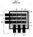
- FIG. 1 illustrates a floor plan of a conventional organic display panel.
- the organic display panel includes a glass substrate 101, an ITO strip 102 formed in a strip form and arrayed in a line on the glass substrate, a supplement electrode 103 formed in a smaller width than the ITO strip on the ITO strip 102, an organic EL layer 104 having a hole transport layer, the emitting layer, and an electron transport layer piled on the ITO strip 102, an insulating film 106 formed between the ITO strip 102 and a bulkhead, an anode strip 105 crossing the ITO strip 102 on the organic EL layer 104 and formed in a band, a bulkhead 107 formed in the band form between the anode strips 105 for separating the neighboring anode strips 105, and a seal-cover 109 coupled to a substrate having the anode strip 105 by using a sealant 108.
- the organic EL display panel is formed in a structure wherein the organic EL layer 104 is inserted between the ITO strip 102 having one higher work function and the anode strip 105 having one lower work function on the glass substrate 101.
- the ITO strip 102 having one higher work function is employed as an anode for injecting the hole and the anode strip 105 having one lower work function is employed as a cathode for injecting the electron.
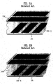
- FIG. 2A to FIG. 2F illustrates a perspective view showing an organic EL display panel in accordance with the related art.
- a transparent ITO strip 102 is formed on the glass substrate 101 for applying the anode.
- an ITO strip 102-A having a short length is also formed between the bulkheads 107 for extracting the anode strip 105 with ease.
- the supplement electrode 103 is formed of such conductive metal as Mo and Cr.
- the sealant 108 on the supplement electrode 103 is not hardened when the sealant 108 is hardened by using UV. Therefore, the width of the supplement electrode 103 at the location where the sealant 108 and the supplement electrode 103 are crossed is set narrower than the ITO strip 102 thereunder.
- the ITO strip 102 further includes the insulating film 106 for insulating the bulkhead 107 from the anode strip 105.
- the insulating film 106 is formed in a blended form of an organic matter, an inorganic matter, and a macromolecule.
- an organic layer 104 is formed on top of the insulating film 106 and the bulkhead 107, and then the anode strip 105 including Mg-Ag compound metal and aluminum or other conductive matter is formed. Finally, the seal-cover 109 is adhered by using the sealant 108.
- FIG. 3 illustrates a floor plan showing an organic EL display panel after the glass substrate and the seal-cover are adhered by using the sealant in accordance with the related art.
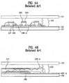
- FIG. 4A illustrates a cross-sectional view of the display panel illustrated in FIG. 3 in accordance with an A direction
- FIG. 4B illustrates a cross-sectional view of the panel illustrated in FIG. 3 in accordance with a B direction.
- the sealant 108 when the sealant 108 is in contact with the bulkhead 107, the sealant 108 is injected along the bulkhead 107 into the emitting cell. Then, the sealant 108-A influences the anode strip and the organic matter, thereby resulting a problem of an inferior emitting cell.
- the present invention is directed to an organic EL (Electroluminescence) display panel that substantially obviates one or more problems due to limitations and disadvantages of the related art.
- An object of the present invention is to provide an organic EL display panel and a manufacturing method of the same for preventing a sealant from being injected along a bulkhead into an emitting cell when a glass substrate and a seal-cover is adhered by using a sealant.
- the organic EL display panel including an emitting cell having an ITO strip, a supplement electrode, an organic EL layer, and an anode strip, and a bulkhead for insulating the emitting cell from the anode strip, being characterized in, the organic EL display panel further including at least one supplement bulkhead for coupling the bulkheads.
- the supplement bulkhead is provided in an area between the emitting cell and the sealant. Desirably, the supplement bulkhead forms a predetermined angle with the bulkhead.
- a method of manufacturing an organic EL display panel includes the steps of forming a supplement electrode in a smaller width than ITO strip, forming an insulating film, forming a bulkhead and at least one supplement bulkhead coupling the bulkheads, forming an organic EL layer and an anode strip, and adhering the seal-cover and the glass substrate by using a sealant.
- the bulkhead and the supplement bulkhead are formed at the same time.
- FIG. 1 illustrates a floor plan of a conventional organic display panel.
- FIG. 2A to FIG. 2F illustrates a perspective view showing an organic EL display panel in accordance with a related art.
- FIG. 3 illustrates a floor plan showing an organic EL display panel after a glass substrate and a seal-cover are adhered by using a sealant in accordance with a related art.
- FIG. 4A illustrates a cross-sectional view of a display panel illustrated in FIG. 3
- FIG. 4B illustrates a cross-sectional view of a panel illustrated in FIG. 3 in accordance with a B direction.
- FIG. 4 illustrates a cross-sectional view of Y direction of an organic display panel in accordance with a related art
- FIG 5A to FIG. 5G illustrate a manufacturing process of an organic EL display panel in accordance with the present invention.
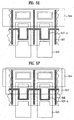
- FIG. 6 illustrates a structure of a supplement bulkhead in accordance with the present invention.
- FIG. 7A to FIG. 7B illustrate various forms of supplement bulkheads in accordance with the present invention.
- FIG. 5A to FIG. 5G illustrate a manufacturing process of an organic EL display panel in accordance with the present invention.
- an ITO strip 512 is formed on a glass substrate 511 for applying an anode.
- an ITO strip 512-A having a short length is formed between bulkheads to be described later at the same time to make it easier to extract an anode strip to be described later.
- a supplement electrode 513 is formed in a smaller width than that of the ITO strip 512 as such a conductive metal as Mo and Cr.
- an insulating film 516 is further formed.
- the insulating film 516 is provided from a predetermined area including a location where a sealant and the supplement electrode 513 are crossed to a portion of the glass substrate 511 around an organic EL display to be described later.
- a bulkhead 517 electrically insulating is provided for insulating between the anode strips to be described later.
- a supplement bulkhead 517-A is further provided for preventing a sealant 518 from being injected along the bulkhead into an emitting cell.
- the supplement bulkhead 517-A is provided at a distance of a from the emitting cell, in a length of b, and inside at a distance of c from an end of the bulkhead 517.
- each of the a, b, c is set larger than 0.
- the supplement bulkhead 517-A is formed in various types of forms.
- the supplement bulkhead 517-A is provided at a predetermined angle (larger than0 and less than 180), not at a right angle.
- the symbol d and d' are an angle between the bulkhead 517 and the supplement bulkhead 517-A.
- the supplement bulkhead 517-A may be formed in many polygonal, circular, and oval forms.
- the sealant is prevented by the bulkhead 517 including more than two supplement bulkheads 517-A.
- the organic EL layer 514 including the hole transport layer, the emitting layer, and the electric transport layer is formed, and then the anode strip 515 including Mg-Ag compound metal, Aluminum or other conductive material is formed.
- the seal-cover 519 is adhered by using the sealant 518 so as to complete the organic El display panel.
- the sealant 518 being injected along the bulkhead is stopped by the supplement bulkhead 517-A.
- the organic EL display panel prevents the sealant 518 from being injected along the bulkhead 517 into the emitting cell by forming the supplement bulkhead 517-A coupling the bulkheads 517 at the end of the bulkhead thereby the inferior device is reduced and the yield is improved.
Landscapes
- Physics & Mathematics (AREA)
- Optics & Photonics (AREA)
- Electroluminescent Light Sources (AREA)
Abstract
Description

Claims (10)
- An organic EL display panel comprising:an emitting cell comprising an ITO strip, a supplement electrode, an organic EL layer, and an anode strip; anda bulkhead for insulating the emitting cell from the anode strip, being characterized in; the organic EL display panel further comprising at least one supplement bulkhead for coupling the bulkheads.
- The organic EL display panel of claim 1, wherein the supplement bulkhead is provided in an area between the emitting cell and the sealant.
- The organic EL display panel of claim 1 or 2, wherein the supplement bulkhead forms a predetermined angle with the bulkhead.
- The organic EL display panel of one of the preceding claims, wherein the supplement bulkhead comprises metal such as Mo and Cr.
- The organic EL display panel of one of the preceding claims, wherein the insulating film is formed around the organic EL layer from a predetermined area including the sealant and the supplement electrode to a portion of the glass substrate.
- The organic EL display panel of one of the preceding claims, wherein the anode strip includes a conductive material such as an alloy of Mg-Ag and aluminum.
- A method of manufacturing an organic EL display panel, comprising the steps of:forming a supplement electrode in a smaller width than ITO strip;forming an insulating film;forming a bulkhead and at least one supplement bulkhead coupling the bulkheads;forming an organic EL layer and an anode strip; andadhering the seal-cover and the glass substrate by using a sealant.
- The organic EL display panel of claim 7, wherein the first step of the process comprises a short ITO strip than the ITO strip between the bulkheads.
- The organic EL display panel of claim 7 or 8, wherein, in the third step of the process, the insulating film is formed around the organic EL layer from a predetermined area including the sealant and the supplement electrode to a portion of the glass substrate.
- The organic EL display panel of one of claims 7 to 9, wherein, in the fourth step of the process, the bulkhead and the supplement bulkhead are formed at the same time.
Applications Claiming Priority (2)
| Application Number | Priority Date | Filing Date | Title |
|---|---|---|---|
| KR2003024103 | 2003-04-16 | ||
| KR10-2003-0024103A KR100499509B1 (en) | 2003-04-16 | 2003-04-16 | Method for Fabricating Polymer Organic Electroluminescence Device |
Publications (2)
| Publication Number | Publication Date |
|---|---|
| EP1469517A2 true EP1469517A2 (en) | 2004-10-20 |
| EP1469517A3 EP1469517A3 (en) | 2006-04-26 |
Family
ID=32906607
Family Applications (1)
| Application Number | Title | Priority Date | Filing Date |
|---|---|---|---|
| EP04008726A Withdrawn EP1469517A3 (en) | 2003-04-16 | 2004-04-13 | Organic electro-luminescence display and manufacturing method threof |
Country Status (5)
| Country | Link |
|---|---|
| US (2) | US7538484B2 (en) |
| EP (1) | EP1469517A3 (en) |
| JP (1) | JP4636305B2 (en) |
| KR (1) | KR100499509B1 (en) |
| CN (1) | CN100578840C (en) |
Families Citing this family (8)
| Publication number | Priority date | Publication date | Assignee | Title |
|---|---|---|---|---|
| KR101032950B1 (en) * | 2004-11-25 | 2011-05-09 | 삼성전자주식회사 | Manufacturing method of organic electroluminescent device |
| JP4795005B2 (en) * | 2004-12-01 | 2011-10-19 | エルジー ディスプレイ カンパニー リミテッド | Organic electroluminescence display device |
| KR100682835B1 (en) * | 2004-12-03 | 2007-02-15 | 엘지전자 주식회사 | Organic electroluminescent device and manufacturing method thereof |
| USD678224S1 (en) * | 2011-02-04 | 2013-03-19 | Panasonic Corporation | Electroluminescence module |
| USD664507S1 (en) * | 2011-02-04 | 2012-07-31 | Panasonic Corporation | Electroluminescence module |
| USD664937S1 (en) * | 2011-02-04 | 2012-08-07 | Panasonic Corporation | Electroluminescence module |
| USD664508S1 (en) * | 2011-02-04 | 2012-07-31 | Panasonic Corporation | Electroluminescence module |
| JP1438220S (en) * | 2011-02-04 | 2015-04-06 |
Family Cites Families (23)
| Publication number | Priority date | Publication date | Assignee | Title |
|---|---|---|---|---|
| FR2541745B1 (en) | 1983-02-28 | 1985-06-21 | Pechiney Aluminium | DEVICE FOR RETAINING A LIQUID PHASE BETWEEN A WALL AND A ROTATING PART THROUGH IT |
| JPS59166224U (en) * | 1983-04-22 | 1984-11-07 | シチズン時計株式会社 | lcd cell |
| JP4142117B2 (en) * | 1995-10-06 | 2008-08-27 | パイオニア株式会社 | Organic electroluminescence display panel and manufacturing method thereof |
| TW420964B (en) * | 1998-02-25 | 2001-02-01 | Toppan Printing Co Ltd | Organic electroluminescence display substrate, method of manufacturing it and organic electroluminescent display element |
| US6603149B2 (en) * | 1998-09-28 | 2003-08-05 | International Business Machines Corporation | Highly efficient OLED device |
| JP4186289B2 (en) * | 1998-12-24 | 2008-11-26 | 凸版印刷株式会社 | Method for producing substrate for organic electroluminescence display element and method for producing organic electroluminescence display element |
| JP2000243555A (en) * | 1999-02-17 | 2000-09-08 | Toyota Motor Corp | Organic EL display |
| JP3736179B2 (en) * | 1999-02-23 | 2006-01-18 | 富士電機ホールディングス株式会社 | Organic thin film light emitting device |
| US6383664B2 (en) | 1999-05-11 | 2002-05-07 | The Dow Chemical Company | Electroluminescent or photocell device having protective packaging |
| JP2001176657A (en) * | 1999-12-16 | 2001-06-29 | Toppan Printing Co Ltd | Substrate for organic electroluminescent display element and organic electroluminescent display element |
| US6624572B1 (en) * | 2000-02-17 | 2003-09-23 | Lg Electronics, Inc. | Organic electroluminescence display panel and method for sealing the same |
| KR100360328B1 (en) * | 2000-02-17 | 2002-11-13 | 엘지전자 주식회사 | Organic Electroluminescence Display Panel |
| JP4478274B2 (en) | 2000-02-17 | 2010-06-09 | 東北パイオニア株式会社 | Organic electroluminescence display panel and manufacturing method thereof |
| JP4004709B2 (en) * | 2000-03-30 | 2007-11-07 | パイオニア株式会社 | Organic electroluminescence display panel and manufacturing method thereof |
| US6838819B2 (en) | 2000-06-19 | 2005-01-04 | Lg Electronics Inc. | Full color organic EL display panel, manufacturing method thereof and driving circuit thereof |
| JP2002008871A (en) * | 2000-06-27 | 2002-01-11 | Tohoku Pioneer Corp | Organic electroluminescence display panel |
| DE10133684A1 (en) * | 2001-07-11 | 2003-02-13 | Osram Opto Semiconductors Gmbh | Organic, colored, electroluminescent display and its manufacture |
| US6656611B2 (en) * | 2001-07-20 | 2003-12-02 | Osram Opto Semiconductors Gmbh | Structure-defining material for OLEDs |
| KR100768182B1 (en) * | 2001-10-26 | 2007-10-17 | 삼성에스디아이 주식회사 | Organic Electroluminescent Device and Manufacturing Method Thereof |
| JP4326799B2 (en) * | 2002-12-27 | 2009-09-09 | 旭テック株式会社 | Cast iron graphite spheroidizing apparatus and cast iron graphite spheroidizing method |
| JP4019944B2 (en) | 2003-01-09 | 2007-12-12 | 株式会社デンソー | Organic EL display device |
| KR100528910B1 (en) * | 2003-01-22 | 2005-11-15 | 삼성에스디아이 주식회사 | Polymer organic light emitting diode |
| KR100843690B1 (en) * | 2006-04-24 | 2008-07-04 | 엘지디스플레이 주식회사 | Light emitting element |
-
2003
- 2003-04-16 KR KR10-2003-0024103A patent/KR100499509B1/en not_active Expired - Fee Related
-
2004
- 2004-04-13 EP EP04008726A patent/EP1469517A3/en not_active Withdrawn
- 2004-04-14 CN CN200410033808A patent/CN100578840C/en not_active Expired - Fee Related
- 2004-04-15 US US10/824,364 patent/US7538484B2/en not_active Expired - Fee Related
- 2004-04-15 JP JP2004120667A patent/JP4636305B2/en not_active Expired - Fee Related
-
2009
- 2009-01-29 US US12/362,228 patent/US8076840B2/en not_active Expired - Fee Related
Also Published As
| Publication number | Publication date |
|---|---|
| US20090200932A1 (en) | 2009-08-13 |
| JP2004319510A (en) | 2004-11-11 |
| US8076840B2 (en) | 2011-12-13 |
| US7538484B2 (en) | 2009-05-26 |
| KR20040090165A (en) | 2004-10-22 |
| EP1469517A3 (en) | 2006-04-26 |
| CN1538790A (en) | 2004-10-20 |
| KR100499509B1 (en) | 2005-07-05 |
| JP4636305B2 (en) | 2011-02-23 |
| US20050007013A1 (en) | 2005-01-13 |
| CN100578840C (en) | 2010-01-06 |
Similar Documents
| Publication | Publication Date | Title |
|---|---|---|
| US6624572B1 (en) | Organic electroluminescence display panel and method for sealing the same | |
| EP0969701B1 (en) | Electroluminescent device | |
| US6917160B2 (en) | Organic electroluminescent display and method of manufacturing the same | |
| US8076840B2 (en) | Organic electro-luminescence display and manufacturing method thereof | |
| KR20080063089A (en) | Organic EL Light Emitting Device and Manufacturing Method Thereof | |
| CN104425761A (en) | White organic light emitting diode and display device using the same | |
| TWI430697B (en) | An organic EL panel, a panel-bonding type light-emitting device, and an organic EL panel | |
| CN1499653A (en) | Organic light emitting diode for display and manufacturing method thereof | |
| CN1366790A (en) | Orgnaic EL display | |
| JP2005157353A (en) | Organic electroluminescent device with low resistance wiring | |
| EP1469518B1 (en) | Organic electroluminescence display panel and method for fabricating the same | |
| CN1638538A (en) | Organic electroluminescent device and method of fabricating the same | |
| KR100528911B1 (en) | Organic electro luminescence display device | |
| US8110979B2 (en) | Inorganic electroluminescence device, display apparatus having the same and method thereof | |
| KR20090029007A (en) | Organic light emitting device and its driving method | |
| EP3098856B1 (en) | Active matrix electroluminescence device and method for fabricating the same | |
| CN1674741B (en) | Organic electro-luminescence device and fabricating method thereof | |
| CN100411222C (en) | Method for manufacturing organic light-emitting display panel and structure | |
| KR100623450B1 (en) | Organic electroluminescent display device and manufacturing method thereof | |
| KR20140088417A (en) | Organic light emitting device | |
| TWI224480B (en) | Method of fabricating organic light emitting diode and structure thereof | |
| US20200194717A1 (en) | Organic light emitting diode display device |
Legal Events
| Date | Code | Title | Description |
|---|---|---|---|
| PUAI | Public reference made under article 153(3) epc to a published international application that has entered the european phase |
Free format text: ORIGINAL CODE: 0009012 |
|
| AK | Designated contracting states |
Kind code of ref document: A2 Designated state(s): AT BE BG CH CY CZ DE DK EE ES FI FR GB GR HU IE IT LI LU MC NL PL PT RO SE SI SK TR |
|
| AX | Request for extension of the european patent |
Extension state: AL HR LT LV MK |
|
| PUAL | Search report despatched |
Free format text: ORIGINAL CODE: 0009013 |
|
| AK | Designated contracting states |
Kind code of ref document: A3 Designated state(s): AT BE BG CH CY CZ DE DK EE ES FI FR GB GR HU IE IT LI LU MC NL PL PT RO SE SI SK TR |
|
| AX | Request for extension of the european patent |
Extension state: AL HR LT LV MK |
|
| 17P | Request for examination filed |
Effective date: 20060902 |
|
| 17Q | First examination report despatched |
Effective date: 20061031 |
|
| AKX | Designation fees paid |
Designated state(s): DE FR GB NL |
|
| STAA | Information on the status of an ep patent application or granted ep patent |
Free format text: STATUS: THE APPLICATION IS DEEMED TO BE WITHDRAWN |
|
| 18D | Application deemed to be withdrawn |
Effective date: 20111129 |