EP1467224A1 - Optische Näherungsschalter - Google Patents
Optische Näherungsschalter Download PDFInfo
- Publication number
- EP1467224A1 EP1467224A1 EP03405233A EP03405233A EP1467224A1 EP 1467224 A1 EP1467224 A1 EP 1467224A1 EP 03405233 A EP03405233 A EP 03405233A EP 03405233 A EP03405233 A EP 03405233A EP 1467224 A1 EP1467224 A1 EP 1467224A1
- Authority
- EP
- European Patent Office
- Prior art keywords
- light
- optical proximity
- proximity detector
- devices
- detecting
- Prior art date
- Legal status (The legal status is an assumption and is not a legal conclusion. Google has not performed a legal analysis and makes no representation as to the accuracy of the status listed.)
- Withdrawn
Links
Images


Classifications
-
- G—PHYSICS
- G01—MEASURING; TESTING
- G01S—RADIO DIRECTION-FINDING; RADIO NAVIGATION; DETERMINING DISTANCE OR VELOCITY BY USE OF RADIO WAVES; LOCATING OR PRESENCE-DETECTING BY USE OF THE REFLECTION OR RERADIATION OF RADIO WAVES; ANALOGOUS ARRANGEMENTS USING OTHER WAVES
- G01S7/00—Details of systems according to groups G01S13/00, G01S15/00, G01S17/00
- G01S7/48—Details of systems according to groups G01S13/00, G01S15/00, G01S17/00 of systems according to group G01S17/00
- G01S7/481—Constructional features, e.g. arrangements of optical elements
- G01S7/4811—Constructional features, e.g. arrangements of optical elements common to transmitter and receiver
-
- G—PHYSICS
- G01—MEASURING; TESTING
- G01S—RADIO DIRECTION-FINDING; RADIO NAVIGATION; DETERMINING DISTANCE OR VELOCITY BY USE OF RADIO WAVES; LOCATING OR PRESENCE-DETECTING BY USE OF THE REFLECTION OR RERADIATION OF RADIO WAVES; ANALOGOUS ARRANGEMENTS USING OTHER WAVES
- G01S17/00—Systems using the reflection or reradiation of electromagnetic waves other than radio waves, e.g. lidar systems
- G01S17/02—Systems using the reflection of electromagnetic waves other than radio waves
- G01S17/04—Systems determining the presence of a target
-
- G—PHYSICS
- G01—MEASURING; TESTING
- G01S—RADIO DIRECTION-FINDING; RADIO NAVIGATION; DETERMINING DISTANCE OR VELOCITY BY USE OF RADIO WAVES; LOCATING OR PRESENCE-DETECTING BY USE OF THE REFLECTION OR RERADIATION OF RADIO WAVES; ANALOGOUS ARRANGEMENTS USING OTHER WAVES
- G01S17/00—Systems using the reflection or reradiation of electromagnetic waves other than radio waves, e.g. lidar systems
- G01S17/87—Combinations of systems using electromagnetic waves other than radio waves
Definitions
- the present invention relates to all sensing and measuring techniques that require a locally resolved detection of the proximity of an object, in order to confirm the presence of the object or to avoid collisions with it. More particularly, it relates to an optical proximity detector according to the preamble of the first claim. Due to the preferably flexible nature of this proximity detector, one can construct "artificial skins" for application to any three-dimensional object, e.g., a car or a robot arm, that requires information about the close-by presence of other objects.
- Touch-sensitive sensors with a deformable front surface are known. However, they require a minimum mechanical deformation or a direct mechanical contact for the detection of the presence of an object. Thus, they cannot detect already the proximity of an object at distances of millimeters or more.
- U.S. Patent No. 5,684,294 describes a proximity and ambient light monitor with a simpler design.
- a light source is modulated with a composite signal
- a photosensor detects a fraction of the light reflected by a close-by object
- an electronic circuit separates the AC component from the detected signal, resulting in reliable proximity detection, also in the presence of ambient light.
- the proximity and ambient light monitor provides for single measurements of ambient light and proximity, as required in the preferred embodiment as a distance monitor for measuring the distance between a headset and a human ear, in a desired target range of 5-25 cm. It does not provide for any local resolution, nor is it flexible.
- U.S. Patent No. 4,564,756 teaches a miniaturized proximity sensor that employs a single light-emitting diode (LED) both as a light source and as a photodetector.
- the LED is forward biased at a fixed voltage, resulting in a certain bias current.
- a disadvantage of this sensor is its reduced sensitivity to reflected light, due to the requirement to measure a small current change in the presence of a relatively large bias current.
- the proximity detector shall be producible at low fabrication costs, and it shall be able to cover large object areas. Ambient light shall not interfere with the measurement process, and the proximity of objects shall be signaled at selectable distance ranges.
- the optical proximity detector comprises a preferably flexible substrate on which a plurality of light-emitting devices and light-detecting devices are arranged. They consist of thin, flexible layers of organic semiconductors and transparent electrodes.
- the light-emitting devices emit continuous or pulsed light, preferably in the visible or near infrared spectral region, through the transparent electrodes.
- An object close to the light-emitting surface of the substrate partially reflects this light, and a fraction of it reaches an adjacent light-detecting device that converts this light into an electrical signal.
- This signal contains information about the proximity of the object, and the information can be extracted with an electronic circuit that is either measuring the amount of detected continuous light or demodulating the detected light pulses. If sufficient reflected light energy is detected, the proximity of an object can be signaled.
- the optical proximity detector comprises a plurality of light-emitting devices for emitting electromagnetic radiation towards an object to be detected, and a plurality of light-detecting devices for detecting electromagnetic radiation emitted by said light-emitting devices and reflected by said object, and for generating an electric signal as a function of said detected radiation. All of said light-emitting devices and light-detecting devices are arranged on a common substrate.
- the substrate of the optical proximity detector is mechanically "flexible" in the sense that it shall be adaptable to the surfaces of three-dimensional objects.
- the flexural strength EI (where E is Young's modulus and I is the geometrical moment of inertia) of the substrate should be smaller than about 10 -2 Nm 2 and may for instance be in the range of about 10 -7 Nm 2 ⁇ EI ⁇ 10 -4 Nm 2 .
- Flexible substrates are preferably used in connection with a special embodiment of the invention in which the light-emitting and light-detecting devices on the substrate are essentially made of organic semiconductor materials.
- the optical proximity detector according to the invention may as well comprise a "rigid" substrate with a flexural strength EI greater than about 10 -2 Nm 2 .
- any substrate may be used for the optical proximity detector according to the invention, from plastic films (such as the well-known Saran Wrap@) to glass-type plates.
- the substrate may be plane or of any other form.
- said light-emitting devices are supplied with drive currents so that each of them emits electromagnetic radiation, and the electric signal generated by at least one light-detecting device adjacent to a light-emitting device supplied with a drive current is read out.
- optical proximity detector according to the invention overcomes the disadvantages of the state of the art in several respects:
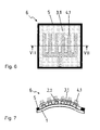
- FIG. 1 A cross section through part of a preferred embodiment of the optical proximity detector 10 according to the invention is shown in Figure 1.
- the detector 10 is based on a preferably flexible substrate 1 made of, e.g., an organic material such as polyester (PET, Mylar®), polyimide (Kapton®), polyamides (Nylon@), polypropylene or polyethylene, of a stainless steel foil, or of other, preferably flexible, materials.
- a preferably flexible substrate 1 made of, e.g., an organic material such as polyester (PET, Mylar®), polyimide (Kapton®), polyamides (Nylon@), polypropylene or polyethylene, of a stainless steel foil, or of other, preferably flexible, materials.
- light-emitting devices 6 and light-detecting devices 8 comprising organic semiconductor layers 3.1, 3.2, respectively, are deposited.
- the light-emitting devices 6 emit light 7 at least into the half-space in which an object 9 shall be detected; the light-detecting devices 8 detect
- the light-emitting device 6 comprises a 10-1000 nm thin layer 3.1 of an organic semiconductor material, sandwiched between a bottom electrode 2.1 and a top electrode 4.1 that are capable of injecting electrons and holes, respectively, into the organic semiconductor 3.1.
- organic semiconductors 3.1 that are suitable for light-emitting devices 6 include PPP - poly (para phenylene), PPV - poly (para phenylene vinylene), Alq 3 - aluminum tris-(8-hydroxyquinoline), tetracene or pentacene.
- Examples of low-work-function electrode materials 2.1 that are capable of injecting electrons include magnesium, calcium and aluminum.
- Examples of high-work-function electrode materials 4.1 that are capable of injecting holes include ITO - indium tin oxide, gold and platinum.
- the light-detecting devices 8 comprises a 10-1000 nm thin layer 3.2 of an organic semiconductor material, sandwiched between a bottom electrode 2.2 and a top electrode 4.2 that are capable of collecting holes and electrons, respectively, into the organic semiconductor 3.2.
- Organic semiconductors 3.2 for high-efficiency light-detecting devices 8 are often polymer blends such as the one described in G. Yu, G. Srdanov, J. Wang, H. Wang, Y. Cao and A. J. Heeger, "Large area, full-color digital image sensors made with semiconducting polymers", Synthetic Metals, Vol. 111-112, pp. 133-137, 2000.
- Examples of low-work-function electrode materials 4.2 that are capable of collecting electrons include magnesium, calcium and aluminum.
- Examples of high-work-function electrode materials 2.2 that are capable of collecting holes include ITO - indium tin oxide, gold and platinum.
- an additional layer (not shown) can be deposited between the organic semiconductor layer 3.1, 3.2 and the electron-injecting/collecting material 2.1 or 4.2.
- Preferred electron-transport materials include PBD - (2-(4-biphenylyle)-5-(4-tert-butyle-phenyle)-1,3,4-oxadiazole and Alq 3 - aluminum tris- (8-hydroxiquinoline).
- an additional layer (not shown) can be deposited between the organic semiconductor layer 3.1, 3.2 and the hole-injecting/collecting material 4.1 or 2.2, such as PEDOT, poly (3,4-ethylenedioxythiophene).
- the electrode material of the light-emitting devices 6 are called “first" top electrode 4.1 or “first” bottom electrode 2.1 and for light-detecting devices 8 “second” top electrode 4.2 or “second” bottom electrode 2.2, or vice versa.
- first organic semiconductor layer 3.1
- second organic semiconductor layer 3.2
- Deposition and patterning of the light-emitting devices 6 and light-detecting devices 8 can be carried out according to fabrication processes well-known in the semiconducting industry, as described for example in S. M. Sze, "Semiconductor Devices - Physics and Technology", 2 nd edition, John Wiley & Sons, Inc., New York, 1992.
- Light-emitting devices 6 and light-detecting devices 8 are preferably placed adjacent to each other, with typical shapes that allow to obtain a good optical fill factor on the substrate 1, as illustrated by means of examples in Figures 2-5.
- a light-emitting device 6 may be allocated to one or several light-detecting devices 8, or vice versa.
- the light-emitting devices 6 and the light-detecting devices 8 are arranged in pairs 11 on the flexible substrate 1.
- Light 7 emitted by a certain light-emitting device 6 and reflected by a near-by object 9 is detected by the light-detecting device 8 belonging to the same pair 11 as said light-emitting device 6. With an arrangement comprising a plurality of such pairs 11, the proximity detection of the object 9 can be locally resolved.
- the optimum size of the light-emitting devices 6 and light-detecting devices 8 depends on the lateral spatial resolution that is desired of the proximity detector 10, and it can vary between a few micrometers up to a few centimeters.
- the detector elements 11 are separated from each other by inter-electrode gaps 20.
- Figure 2 shows an arrangement of square (or rectangular) detector elements 11, each element 11 comprising a central square (or rectangular) light-emitting device 6 and a surrounding light-detecting device 8.
- Figure 3 shows an arrangement of circular detector elements 11, each element 11 comprising a central circular light-emitting device 6 and a surrounding light-detecting device 8.
- Figure 4 shows an arrangement of hexagonal detector elements 11.
- Figure 5 shows an arrangement of square (or rectangular) detector elements 11, each element comprising a square (or rectangular) light-emitting device 6 and an adjacent L-shaped light-detecting device 8.
- Emitted light 7 (cf. Fig. 1) must be able to escape from the organic semiconductor layer 3 into free space, and light reflected by the object 9 must enter the organic semiconductor layer 3 in order to be detected.
- four measures (i)-(iv) may be taken, separately or in combination with each other, for this purpose:
- an optical shielding 5 is provided.
- This shielding 5 consists of optically opaque material that is deposited in such a way between all of the devices 6, 8 fabricated on the flexible substrate 1 that no light can be transmitted laterally.
- the optical shielding 5 is preferably also an electrical insulator which prevents that electrical connections are created between the devices 6, 8.
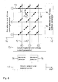
- the light-emitting devices 6 and the light-detecting devices 8 that are arranged on the flexible substrate 1 are preferably provided with a grid of control lines 12, 12', 13, 13', leading to the perimeter of the substrate 1, with which the devices 6, 8 of the optical proximity detector are operated.
- a grid of control lines 12, 12', 13, 13' leading to the perimeter of the substrate 1, with which the devices 6, 8 of the optical proximity detector are operated.
- Such an arrangement of lines 12, 12', 13, 13' and electronic circuits 14, 14', 15-17 for the multiplexed operation of the optical proximity detector 10 is illustrated in Figure 8.
- the light-emitting devices 6 are provided with vertical or column lines 12 connected to their cathodes and horizontal or row lines 13 connected to their anodes.
- the row lines 13 are connected to an electronic circuit 14 for row selection and bias current generation providing the following function: all rows are kept at negative potential except one row that is switched to positive potential.
- the column lines 12 are connected to an electronic circuit 15 for column selection and bias current generation providing the following function: all columns are kept at positive potential except one column that is switched to negative potential.
- the light-emitting device 6 at the cross point of the positive row line 13 and the negative column line 12 will light up, and it is the function of the bias current generator either to stabilize the current through the corresponding light-emitting device 6 or to modulate the current.
- Each light-emitting device 6 can be individually addressed by the row-selector circuit 14 in combination with the column-selector circuit 15; the light-emitting devices 6 can be scanned sequentially or in an arbitrary manner.
- the light-detecting devices 8 are provided with vertical or column lines 12' connected to their anodes and horizontal or row lines 13' connected to their cathodes.
- the horizontal lines 13' are connected to an electronic circuit 14' for row selection and bias voltage generation.
- the optimum bias voltage is such that anodes and cathodes of the light-detecting devices 8 are kept at the same potential.
- different electronic detector circuits 16 are employed at the column lines 12':
- FIG. 12(a) shows a conventional connection of a light-detecting device 8 to a vertical line 12'and a horizontal line 13'.
- the anode of each light-detecting device 8 is connected to its column line 12' via a control transistor 18, e.g., a field-effect transistor (FET), the gate of which is controlled by a control voltage applied to an additional control line 19'.
- FET field-effect transistor
Landscapes
- Engineering & Computer Science (AREA)
- Physics & Mathematics (AREA)
- Computer Networks & Wireless Communication (AREA)
- General Physics & Mathematics (AREA)
- Radar, Positioning & Navigation (AREA)
- Remote Sensing (AREA)
- Electromagnetism (AREA)
- Electroluminescent Light Sources (AREA)
Priority Applications (1)
| Application Number | Priority Date | Filing Date | Title |
|---|---|---|---|
| EP03405233A EP1467224A1 (de) | 2003-04-07 | 2003-04-07 | Optische Näherungsschalter |
Applications Claiming Priority (1)
| Application Number | Priority Date | Filing Date | Title |
|---|---|---|---|
| EP03405233A EP1467224A1 (de) | 2003-04-07 | 2003-04-07 | Optische Näherungsschalter |
Publications (1)
| Publication Number | Publication Date |
|---|---|
| EP1467224A1 true EP1467224A1 (de) | 2004-10-13 |
Family
ID=32865097
Family Applications (1)
| Application Number | Title | Priority Date | Filing Date |
|---|---|---|---|
| EP03405233A Withdrawn EP1467224A1 (de) | 2003-04-07 | 2003-04-07 | Optische Näherungsschalter |
Country Status (1)
| Country | Link |
|---|---|
| EP (1) | EP1467224A1 (de) |
Cited By (33)
| Publication number | Priority date | Publication date | Assignee | Title |
|---|---|---|---|---|
| EP1689291A1 (de) * | 2003-11-18 | 2006-08-16 | Qinetiq Limited | Flexible lichtquellen und detektoren und ihre anwendungen |
| WO2009035324A1 (en) | 2007-09-10 | 2009-03-19 | Nederlandse Organisatie Voor Toegepast-Natuurwetenschappelijk Onderzoek Tno | Optical sensor for measuring a force distribution |
| DE102009042609A1 (de) * | 2009-09-23 | 2011-03-24 | Siemens Aktiengesellschaft | Optischer Sensor, insbesondere Näherungsschalter |
| WO2011038968A1 (de) * | 2009-10-01 | 2011-04-07 | Robert Bosch Gmbh | Sensoreinrichtung und deren verwendung |
| WO2011112931A1 (en) * | 2010-03-12 | 2011-09-15 | The Board Of Trustees Of The University Of Illinois | Waterproof stretchable optoelectronics |
| US8372726B2 (en) | 2008-10-07 | 2013-02-12 | Mc10, Inc. | Methods and applications of non-planar imaging arrays |
| US8389862B2 (en) | 2008-10-07 | 2013-03-05 | Mc10, Inc. | Extremely stretchable electronics |
| US8440546B2 (en) | 2004-06-04 | 2013-05-14 | The Board Of Trustees Of The University Of Illinois | Methods and devices for fabricating and assembling printable semiconductor elements |
| US8529835B2 (en) | 2006-11-03 | 2013-09-10 | Tufts University | Biopolymer sensor and method of manufacturing the same |
| US8536667B2 (en) | 2008-10-07 | 2013-09-17 | Mc10, Inc. | Systems, methods, and devices having stretchable integrated circuitry for sensing and delivering therapy |
| US8574461B2 (en) | 2006-11-03 | 2013-11-05 | Tufts University | Electroactive biopolymer optical and electro-optical devices and method of manufacturing the same |
| US8666471B2 (en) | 2010-03-17 | 2014-03-04 | The Board Of Trustees Of The University Of Illinois | Implantable biomedical devices on bioresorbable substrates |
| US8747886B2 (en) | 2009-02-12 | 2014-06-10 | Tufts University | Nanoimprinting of silk fibroin structures for biomedical and biophotonic applications |
| US8886334B2 (en) | 2008-10-07 | 2014-11-11 | Mc10, Inc. | Systems, methods, and devices using stretchable or flexible electronics for medical applications |
| US8934965B2 (en) | 2011-06-03 | 2015-01-13 | The Board Of Trustees Of The University Of Illinois | Conformable actively multiplexed high-density surface electrode array for brain interfacing |
| US8969784B2 (en) | 2012-05-14 | 2015-03-03 | Avago Technologies General Ip (Singapore) Pte. Ltd. | Optical lens assembly and optical devices thereof |
| US9016875B2 (en) | 2009-07-20 | 2015-04-28 | Tufts University/Trustees Of Tufts College | All-protein implantable, resorbable reflectors |
| US9142787B2 (en) | 2009-08-31 | 2015-09-22 | Tufts University | Silk transistor devices |
| US9159635B2 (en) | 2011-05-27 | 2015-10-13 | Mc10, Inc. | Flexible electronic structure |
| US9171794B2 (en) | 2012-10-09 | 2015-10-27 | Mc10, Inc. | Embedding thin chips in polymer |
| US9289132B2 (en) | 2008-10-07 | 2016-03-22 | Mc10, Inc. | Catheter balloon having stretchable integrated circuitry and sensor array |
| US9513405B2 (en) | 2006-11-03 | 2016-12-06 | Tufts University | Biopolymer photonic crystals and method of manufacturing the same |
| US9554484B2 (en) | 2012-03-30 | 2017-01-24 | The Board Of Trustees Of The University Of Illinois | Appendage mountable electronic devices conformable to surfaces |
| US9599891B2 (en) | 2007-11-05 | 2017-03-21 | Trustees Of Tufts College | Fabrication of silk fibroin photonic structures by nanocontact imprinting |
| US9691873B2 (en) | 2011-12-01 | 2017-06-27 | The Board Of Trustees Of The University Of Illinois | Transient devices designed to undergo programmable transformations |
| US9723122B2 (en) | 2009-10-01 | 2017-08-01 | Mc10, Inc. | Protective cases with integrated electronics |
| US9765934B2 (en) | 2011-05-16 | 2017-09-19 | The Board Of Trustees Of The University Of Illinois | Thermally managed LED arrays assembled by printing |
| US9936574B2 (en) | 2009-12-16 | 2018-04-03 | The Board Of Trustees Of The University Of Illinois | Waterproof stretchable optoelectronics |
| US9969134B2 (en) | 2006-11-03 | 2018-05-15 | Trustees Of Tufts College | Nanopatterned biopolymer optical device and method of manufacturing the same |
| JP2019075557A (ja) * | 2017-10-11 | 2019-05-16 | 三星電子株式会社Samsung Electronics Co.,Ltd. | 光源一体型光センシングシステム、及びそれを含む電子機器 |
| US10441185B2 (en) | 2009-12-16 | 2019-10-15 | The Board Of Trustees Of The University Of Illinois | Flexible and stretchable electronic systems for epidermal electronics |
| US10918298B2 (en) | 2009-12-16 | 2021-02-16 | The Board Of Trustees Of The University Of Illinois | High-speed, high-resolution electrophysiology in-vivo using conformal electronics |
| US10925543B2 (en) | 2015-11-11 | 2021-02-23 | The Board Of Trustees Of The University Of Illinois | Bioresorbable silicon electronics for transient implants |
Citations (5)
| Publication number | Priority date | Publication date | Assignee | Title |
|---|---|---|---|---|
| US5684294A (en) | 1996-10-17 | 1997-11-04 | Northern Telecom Ltd | Proximity and ambient light monitor |
| GB2315594A (en) | 1996-07-22 | 1998-02-04 | Cambridge Display Tech Ltd | Sensing device comprising coplanar light emitter and detectors |
| EP0949696A2 (de) * | 1998-04-08 | 1999-10-13 | Idemitsu Kosan Company Limited | Organische elektrolumineszente Vorrichtung |
| US6023064A (en) * | 1994-12-08 | 2000-02-08 | U.K. Robotics Limited | Object sensing system |
| WO2002091319A2 (en) * | 2001-05-04 | 2002-11-14 | Igt | Light emitting interface displays for a gaming machine |
-
2003
- 2003-04-07 EP EP03405233A patent/EP1467224A1/de not_active Withdrawn
Patent Citations (5)
| Publication number | Priority date | Publication date | Assignee | Title |
|---|---|---|---|---|
| US6023064A (en) * | 1994-12-08 | 2000-02-08 | U.K. Robotics Limited | Object sensing system |
| GB2315594A (en) | 1996-07-22 | 1998-02-04 | Cambridge Display Tech Ltd | Sensing device comprising coplanar light emitter and detectors |
| US5684294A (en) | 1996-10-17 | 1997-11-04 | Northern Telecom Ltd | Proximity and ambient light monitor |
| EP0949696A2 (de) * | 1998-04-08 | 1999-10-13 | Idemitsu Kosan Company Limited | Organische elektrolumineszente Vorrichtung |
| WO2002091319A2 (en) * | 2001-05-04 | 2002-11-14 | Igt | Light emitting interface displays for a gaming machine |
Non-Patent Citations (2)
| Title |
|---|
| LUMELSKY V J ET AL: "Sensitive skin", IEEE SENSORS JOURNAL, JUNE 2001, IEEE, USA, vol. 1, no. 1, pages 41 - 51, XP002254115, ISSN: 1530-437X * |
| LUMELSKY V. J. ET AL.: "Sensitive Skin", IEEE SENSORS JOURNAL, vol. 1, no. 1, June 2001 (2001-06-01), pages 41 - 51 |
Cited By (59)
| Publication number | Priority date | Publication date | Assignee | Title |
|---|---|---|---|---|
| EP1689291A1 (de) * | 2003-11-18 | 2006-08-16 | Qinetiq Limited | Flexible lichtquellen und detektoren und ihre anwendungen |
| US8664699B2 (en) | 2004-06-04 | 2014-03-04 | The Board Of Trustees Of The University Of Illinois | Methods and devices for fabricating and assembling printable semiconductor elements |
| US9761444B2 (en) | 2004-06-04 | 2017-09-12 | The Board Of Trustees Of The University Of Illinois | Methods and devices for fabricating and assembling printable semiconductor elements |
| US9768086B2 (en) | 2004-06-04 | 2017-09-19 | The Board Of Trustees Of The University Of Illinois | Methods and devices for fabricating and assembling printable semiconductor elements |
| US12074213B2 (en) | 2004-06-04 | 2024-08-27 | The Board Of Trustees Of The University Of Illinois | Methods and devices for fabricating and assembling printable semiconductor elements |
| US11088268B2 (en) | 2004-06-04 | 2021-08-10 | The Board Of Trustees Of The University Of Illinois | Methods and devices for fabricating and assembling printable semiconductor elements |
| US10374072B2 (en) | 2004-06-04 | 2019-08-06 | The Board Of Trustees Of The University Of Illinois | Methods and devices for fabricating and assembling printable semiconductor elements |
| US9450043B2 (en) | 2004-06-04 | 2016-09-20 | The Board Of Trustees Of The University Of Illinois | Methods and devices for fabricating and assembling printable semiconductor elements |
| US8440546B2 (en) | 2004-06-04 | 2013-05-14 | The Board Of Trustees Of The University Of Illinois | Methods and devices for fabricating and assembling printable semiconductor elements |
| US9969134B2 (en) | 2006-11-03 | 2018-05-15 | Trustees Of Tufts College | Nanopatterned biopolymer optical device and method of manufacturing the same |
| US8574461B2 (en) | 2006-11-03 | 2013-11-05 | Tufts University | Electroactive biopolymer optical and electro-optical devices and method of manufacturing the same |
| US8529835B2 (en) | 2006-11-03 | 2013-09-10 | Tufts University | Biopolymer sensor and method of manufacturing the same |
| US10280204B2 (en) | 2006-11-03 | 2019-05-07 | Tufts University | Electroactive biopolymer optical and electro-optical devices and method of manufacturing the same |
| US9513405B2 (en) | 2006-11-03 | 2016-12-06 | Tufts University | Biopolymer photonic crystals and method of manufacturing the same |
| US10040834B2 (en) | 2006-11-03 | 2018-08-07 | Tufts University | Biopolymer optofluidic device and method of manufacturing the same |
| US9802374B2 (en) | 2006-11-03 | 2017-10-31 | Tufts University | Biopolymer sensor and method of manufacturing the same |
| JP2010539474A (ja) * | 2007-09-10 | 2010-12-16 | ネーデルランデ オルガニサティー ヴール トゥーヘパストナツールウェテンスハペライク オンデルズーク テーエヌオー | 力分布測定用光学センサ |
| US8749522B2 (en) | 2007-09-10 | 2014-06-10 | Nederlandse Organisatie Voor Toegepast-Natuurwetenschappelijk Onderzoek Tno | Optical sensor for measuring a force distribution |
| WO2009035324A1 (en) | 2007-09-10 | 2009-03-19 | Nederlandse Organisatie Voor Toegepast-Natuurwetenschappelijk Onderzoek Tno | Optical sensor for measuring a force distribution |
| US9599891B2 (en) | 2007-11-05 | 2017-03-21 | Trustees Of Tufts College | Fabrication of silk fibroin photonic structures by nanocontact imprinting |
| US8389862B2 (en) | 2008-10-07 | 2013-03-05 | Mc10, Inc. | Extremely stretchable electronics |
| US9012784B2 (en) | 2008-10-07 | 2015-04-21 | Mc10, Inc. | Extremely stretchable electronics |
| US8372726B2 (en) | 2008-10-07 | 2013-02-12 | Mc10, Inc. | Methods and applications of non-planar imaging arrays |
| US8886334B2 (en) | 2008-10-07 | 2014-11-11 | Mc10, Inc. | Systems, methods, and devices using stretchable or flexible electronics for medical applications |
| US8536667B2 (en) | 2008-10-07 | 2013-09-17 | Mc10, Inc. | Systems, methods, and devices having stretchable integrated circuitry for sensing and delivering therapy |
| US9289132B2 (en) | 2008-10-07 | 2016-03-22 | Mc10, Inc. | Catheter balloon having stretchable integrated circuitry and sensor array |
| US8747886B2 (en) | 2009-02-12 | 2014-06-10 | Tufts University | Nanoimprinting of silk fibroin structures for biomedical and biophotonic applications |
| US9603810B2 (en) | 2009-02-12 | 2017-03-28 | Tufts University | Nanoimprinting of silk fibroin structures for biomedical and biophotonic applications |
| US9016875B2 (en) | 2009-07-20 | 2015-04-28 | Tufts University/Trustees Of Tufts College | All-protein implantable, resorbable reflectors |
| US9142787B2 (en) | 2009-08-31 | 2015-09-22 | Tufts University | Silk transistor devices |
| DE102009042609A1 (de) * | 2009-09-23 | 2011-03-24 | Siemens Aktiengesellschaft | Optischer Sensor, insbesondere Näherungsschalter |
| US8841598B2 (en) | 2009-09-23 | 2014-09-23 | Siemens Aktiengesellschaft | Optical sensor comprising a proximity switch |
| EP2481152B1 (de) * | 2009-09-23 | 2018-07-04 | Siemens Healthcare GmbH | Optischer sensor, insbesondere näherungsschalter |
| WO2011038968A1 (de) * | 2009-10-01 | 2011-04-07 | Robert Bosch Gmbh | Sensoreinrichtung und deren verwendung |
| US9723122B2 (en) | 2009-10-01 | 2017-08-01 | Mc10, Inc. | Protective cases with integrated electronics |
| US10441185B2 (en) | 2009-12-16 | 2019-10-15 | The Board Of Trustees Of The University Of Illinois | Flexible and stretchable electronic systems for epidermal electronics |
| US9936574B2 (en) | 2009-12-16 | 2018-04-03 | The Board Of Trustees Of The University Of Illinois | Waterproof stretchable optoelectronics |
| US10918298B2 (en) | 2009-12-16 | 2021-02-16 | The Board Of Trustees Of The University Of Illinois | High-speed, high-resolution electrophysiology in-vivo using conformal electronics |
| US11057991B2 (en) | 2009-12-16 | 2021-07-06 | The Board Of Trustees Of The University Of Illinois | Waterproof stretchable optoelectronics |
| TWI646988B (zh) * | 2010-03-12 | 2019-01-11 | 美國伊利諾大學理事會 | 生物醫學裝置及其製造方法、流體遞送監視器、監視在管子中流動之流體的方法、近接感測器及感測兩個物件之間的距離的方法 |
| TWI623063B (zh) * | 2010-03-12 | 2018-05-01 | 美國伊利諾大學理事會 | 生物醫學裝置及其製造方法、流體遞送監視器、監視在管子中流動之流體的方法、近接感測器及感測兩個物件之間的距離的方法 |
| EP3695792A1 (de) | 2010-03-12 | 2020-08-19 | The Board of Trustees of the University of Illinois | Wasserfeste dehnbare optoelektronische elemente |
| WO2011112931A1 (en) * | 2010-03-12 | 2011-09-15 | The Board Of Trustees Of The University Of Illinois | Waterproof stretchable optoelectronics |
| US9986924B2 (en) | 2010-03-17 | 2018-06-05 | The Board Of Trustees Of The University Of Illinois | Implantable biomedical devices on bioresorbable substrates |
| US8666471B2 (en) | 2010-03-17 | 2014-03-04 | The Board Of Trustees Of The University Of Illinois | Implantable biomedical devices on bioresorbable substrates |
| US9765934B2 (en) | 2011-05-16 | 2017-09-19 | The Board Of Trustees Of The University Of Illinois | Thermally managed LED arrays assembled by printing |
| US9159635B2 (en) | 2011-05-27 | 2015-10-13 | Mc10, Inc. | Flexible electronic structure |
| US10349860B2 (en) | 2011-06-03 | 2019-07-16 | The Board Of Trustees Of The University Of Illinois | Conformable actively multiplexed high-density surface electrode array for brain interfacing |
| US8934965B2 (en) | 2011-06-03 | 2015-01-13 | The Board Of Trustees Of The University Of Illinois | Conformable actively multiplexed high-density surface electrode array for brain interfacing |
| US9691873B2 (en) | 2011-12-01 | 2017-06-27 | The Board Of Trustees Of The University Of Illinois | Transient devices designed to undergo programmable transformations |
| US10396173B2 (en) | 2011-12-01 | 2019-08-27 | The Board Of Trustees Of The University Of Illinois | Transient devices designed to undergo programmable transformations |
| US10052066B2 (en) | 2012-03-30 | 2018-08-21 | The Board Of Trustees Of The University Of Illinois | Appendage mountable electronic devices conformable to surfaces |
| US9554484B2 (en) | 2012-03-30 | 2017-01-24 | The Board Of Trustees Of The University Of Illinois | Appendage mountable electronic devices conformable to surfaces |
| US10357201B2 (en) | 2012-03-30 | 2019-07-23 | The Board Of Trustees Of The University Of Illinois | Appendage mountable electronic devices conformable to surfaces |
| US8969784B2 (en) | 2012-05-14 | 2015-03-03 | Avago Technologies General Ip (Singapore) Pte. Ltd. | Optical lens assembly and optical devices thereof |
| US9171794B2 (en) | 2012-10-09 | 2015-10-27 | Mc10, Inc. | Embedding thin chips in polymer |
| US10925543B2 (en) | 2015-11-11 | 2021-02-23 | The Board Of Trustees Of The University Of Illinois | Bioresorbable silicon electronics for transient implants |
| US11749775B2 (en) | 2017-10-11 | 2023-09-05 | Samsung Electronics Co., Ltd. | Light source-integrated light sensing system and electronic device including the same |
| JP2019075557A (ja) * | 2017-10-11 | 2019-05-16 | 三星電子株式会社Samsung Electronics Co.,Ltd. | 光源一体型光センシングシステム、及びそれを含む電子機器 |
Similar Documents
| Publication | Publication Date | Title |
|---|---|---|
| EP1467224A1 (de) | Optische Näherungsschalter | |
| CN110603579B (zh) | 图像采集系统 | |
| KR102687203B1 (ko) | 수광화소영역을 포함하는 표시장치 | |
| US10990789B2 (en) | Display apparatus including light-receiving pixel area | |
| US8399821B2 (en) | Light source integrated photoelectric conversion apparatus | |
| US20180231376A1 (en) | Detector for an optical detection of at least one object | |
| JP5093844B2 (ja) | 集積有機発光素子を備えるリフレックスカプラ | |
| US20100220041A1 (en) | Optoelectronic Device | |
| TWI384666B (zh) | Light detection device structure | |
| KR20180085227A (ko) | 광학식 지문센싱 장치 및 이를 포함하는 터치 디바이스 | |
| US20180240843A1 (en) | Print sensor with gallium nitride led | |
| US20220037410A1 (en) | Detection device | |
| US20080031501A1 (en) | Fingerprinting Device | |
| KR102636405B1 (ko) | 수광화소영역을 포함하는 표시장치 | |
| US10461129B2 (en) | Device for detecting electromagnetic radiation consisting of organic materials | |
| WO2022038042A1 (en) | Display and method for manufacturing a display | |
| CN116134620A (zh) | 检测装置 | |
| WO2012164259A1 (en) | Electronic devices | |
| CN113711266A (zh) | 检测装置 | |
| KR20230024851A (ko) | 감지 디바이스 및 전자 디바이스 | |
| WO2022038037A1 (en) | Electronic sensing device and sensing method | |
| WO2000060530A1 (en) | Planar optical image sensor and system for generating an electronic image of a relief object for fingerprint reading | |
| WO2024185478A1 (ja) | 検出装置 | |
| EP3885971B1 (de) | Lichtemitter-/-sensoreinheit, anzeige und verfahren zur herstellung einer anzeige | |
| WO2024135768A1 (ja) | 検出装置 |
Legal Events
| Date | Code | Title | Description |
|---|---|---|---|
| PUAI | Public reference made under article 153(3) epc to a published international application that has entered the european phase |
Free format text: ORIGINAL CODE: 0009012 |
|
| AK | Designated contracting states |
Kind code of ref document: A1 Designated state(s): AT BE BG CH CY CZ DE DK EE ES FI FR GB GR HU IE IT LI LU MC NL PT RO SE SI SK TR |
|
| AX | Request for extension of the european patent |
Extension state: AL LT LV MK |
|
| 17P | Request for examination filed |
Effective date: 20041201 |
|
| AKX | Designation fees paid |
Designated state(s): CH DE FR GB LI |
|
| RAP1 | Party data changed (applicant data changed or rights of an application transferred) |
Owner name: CSEM CENTRE SUISSE D'ELECTRONIQUE ET DE MICROTECHN |
|
| STAA | Information on the status of an ep patent application or granted ep patent |
Free format text: STATUS: THE APPLICATION IS DEEMED TO BE WITHDRAWN |
|
| 18D | Application deemed to be withdrawn |
Effective date: 20161101 |