EP1465244A2 - Integrated circuit package with exposed die surfaces and auxiliary attachment - Google Patents
Integrated circuit package with exposed die surfaces and auxiliary attachment Download PDFInfo
- Publication number
- EP1465244A2 EP1465244A2 EP04251766A EP04251766A EP1465244A2 EP 1465244 A2 EP1465244 A2 EP 1465244A2 EP 04251766 A EP04251766 A EP 04251766A EP 04251766 A EP04251766 A EP 04251766A EP 1465244 A2 EP1465244 A2 EP 1465244A2
- Authority
- EP
- European Patent Office
- Prior art keywords
- die
- integrated circuit
- package
- exposed
- auxiliary component
- Prior art date
- Legal status (The legal status is an assumption and is not a legal conclusion. Google has not performed a legal analysis and makes no representation as to the accuracy of the status listed.)
- Granted
Links
Images


Classifications
-
- G—PHYSICS
- G06—COMPUTING OR CALCULATING; COUNTING
- G06V—IMAGE OR VIDEO RECOGNITION OR UNDERSTANDING
- G06V40/00—Recognition of biometric, human-related or animal-related patterns in image or video data
- G06V40/10—Human or animal bodies, e.g. vehicle occupants or pedestrians; Body parts, e.g. hands
- G06V40/12—Fingerprints or palmprints
- G06V40/13—Sensors therefor
- G06V40/1306—Sensors therefor non-optical, e.g. ultrasonic or capacitive sensing
-
- H—ELECTRICITY
- H10—SEMICONDUCTOR DEVICES; ELECTRIC SOLID-STATE DEVICES NOT OTHERWISE PROVIDED FOR
- H10W—GENERIC PACKAGES, INTERCONNECTIONS, CONNECTORS OR OTHER CONSTRUCTIONAL DETAILS OF DEVICES COVERED BY CLASS H10
- H10W74/00—Encapsulations, e.g. protective coatings
- H10W74/01—Manufacture or treatment
- H10W74/016—Manufacture or treatment using moulds
-
- H—ELECTRICITY
- H10—SEMICONDUCTOR DEVICES; ELECTRIC SOLID-STATE DEVICES NOT OTHERWISE PROVIDED FOR
- H10W—GENERIC PACKAGES, INTERCONNECTIONS, CONNECTORS OR OTHER CONSTRUCTIONAL DETAILS OF DEVICES COVERED BY CLASS H10
- H10W74/00—Encapsulations, e.g. protective coatings
- H10W74/10—Encapsulations, e.g. protective coatings characterised by their shape or disposition
- H10W74/111—Encapsulations, e.g. protective coatings characterised by their shape or disposition the semiconductor body being completely enclosed
-
- H—ELECTRICITY
- H10—SEMICONDUCTOR DEVICES; ELECTRIC SOLID-STATE DEVICES NOT OTHERWISE PROVIDED FOR
- H10W—GENERIC PACKAGES, INTERCONNECTIONS, CONNECTORS OR OTHER CONSTRUCTIONAL DETAILS OF DEVICES COVERED BY CLASS H10
- H10W72/00—Interconnections or connectors in packages
- H10W72/071—Connecting or disconnecting
- H10W72/075—Connecting or disconnecting of bond wires
-
- H—ELECTRICITY
- H10—SEMICONDUCTOR DEVICES; ELECTRIC SOLID-STATE DEVICES NOT OTHERWISE PROVIDED FOR
- H10W—GENERIC PACKAGES, INTERCONNECTIONS, CONNECTORS OR OTHER CONSTRUCTIONAL DETAILS OF DEVICES COVERED BY CLASS H10
- H10W72/00—Interconnections or connectors in packages
- H10W72/071—Connecting or disconnecting
- H10W72/075—Connecting or disconnecting of bond wires
- H10W72/07511—Treating the bonding area before connecting, e.g. by applying flux or cleaning
-
- H—ELECTRICITY
- H10—SEMICONDUCTOR DEVICES; ELECTRIC SOLID-STATE DEVICES NOT OTHERWISE PROVIDED FOR
- H10W—GENERIC PACKAGES, INTERCONNECTIONS, CONNECTORS OR OTHER CONSTRUCTIONAL DETAILS OF DEVICES COVERED BY CLASS H10
- H10W72/00—Interconnections or connectors in packages
- H10W72/20—Bump connectors, e.g. solder bumps or copper pillars; Dummy bumps; Thermal bumps
- H10W72/29—Bond pads specially adapted therefor
-
- H—ELECTRICITY
- H10—SEMICONDUCTOR DEVICES; ELECTRIC SOLID-STATE DEVICES NOT OTHERWISE PROVIDED FOR
- H10W—GENERIC PACKAGES, INTERCONNECTIONS, CONNECTORS OR OTHER CONSTRUCTIONAL DETAILS OF DEVICES COVERED BY CLASS H10
- H10W72/00—Interconnections or connectors in packages
- H10W72/50—Bond wires
- H10W72/531—Shapes of wire connectors
- H10W72/536—Shapes of wire connectors the connected ends being ball-shaped
-
- H—ELECTRICITY
- H10—SEMICONDUCTOR DEVICES; ELECTRIC SOLID-STATE DEVICES NOT OTHERWISE PROVIDED FOR
- H10W—GENERIC PACKAGES, INTERCONNECTIONS, CONNECTORS OR OTHER CONSTRUCTIONAL DETAILS OF DEVICES COVERED BY CLASS H10
- H10W72/00—Interconnections or connectors in packages
- H10W72/50—Bond wires
- H10W72/531—Shapes of wire connectors
- H10W72/5363—Shapes of wire connectors the connected ends being wedge-shaped
-
- H—ELECTRICITY
- H10—SEMICONDUCTOR DEVICES; ELECTRIC SOLID-STATE DEVICES NOT OTHERWISE PROVIDED FOR
- H10W—GENERIC PACKAGES, INTERCONNECTIONS, CONNECTORS OR OTHER CONSTRUCTIONAL DETAILS OF DEVICES COVERED BY CLASS H10
- H10W72/00—Interconnections or connectors in packages
- H10W72/50—Bond wires
- H10W72/541—Dispositions of bond wires
- H10W72/5434—Dispositions of bond wires the connected ends being on auxiliary connecting means on bond pads, e.g. on other bond wires
-
- H—ELECTRICITY
- H10—SEMICONDUCTOR DEVICES; ELECTRIC SOLID-STATE DEVICES NOT OTHERWISE PROVIDED FOR
- H10W—GENERIC PACKAGES, INTERCONNECTIONS, CONNECTORS OR OTHER CONSTRUCTIONAL DETAILS OF DEVICES COVERED BY CLASS H10
- H10W72/00—Interconnections or connectors in packages
- H10W72/90—Bond pads, in general
- H10W72/951—Materials of bond pads
-
- H—ELECTRICITY
- H10—SEMICONDUCTOR DEVICES; ELECTRIC SOLID-STATE DEVICES NOT OTHERWISE PROVIDED FOR
- H10W—GENERIC PACKAGES, INTERCONNECTIONS, CONNECTORS OR OTHER CONSTRUCTIONAL DETAILS OF DEVICES COVERED BY CLASS H10
- H10W74/00—Encapsulations, e.g. protective coatings
-
- H—ELECTRICITY
- H10—SEMICONDUCTOR DEVICES; ELECTRIC SOLID-STATE DEVICES NOT OTHERWISE PROVIDED FOR
- H10W—GENERIC PACKAGES, INTERCONNECTIONS, CONNECTORS OR OTHER CONSTRUCTIONAL DETAILS OF DEVICES COVERED BY CLASS H10
- H10W74/00—Encapsulations, e.g. protective coatings
- H10W74/10—Encapsulations, e.g. protective coatings characterised by their shape or disposition
-
- H—ELECTRICITY
- H10—SEMICONDUCTOR DEVICES; ELECTRIC SOLID-STATE DEVICES NOT OTHERWISE PROVIDED FOR
- H10W—GENERIC PACKAGES, INTERCONNECTIONS, CONNECTORS OR OTHER CONSTRUCTIONAL DETAILS OF DEVICES COVERED BY CLASS H10
- H10W90/00—Package configurations
- H10W90/701—Package configurations characterised by the relative positions of pads or connectors relative to package parts
- H10W90/721—Package configurations characterised by the relative positions of pads or connectors relative to package parts of bump connectors
- H10W90/722—Package configurations characterised by the relative positions of pads or connectors relative to package parts of bump connectors between stacked chips
-
- H—ELECTRICITY
- H10—SEMICONDUCTOR DEVICES; ELECTRIC SOLID-STATE DEVICES NOT OTHERWISE PROVIDED FOR
- H10W—GENERIC PACKAGES, INTERCONNECTIONS, CONNECTORS OR OTHER CONSTRUCTIONAL DETAILS OF DEVICES COVERED BY CLASS H10
- H10W90/00—Package configurations
- H10W90/701—Package configurations characterised by the relative positions of pads or connectors relative to package parts
- H10W90/751—Package configurations characterised by the relative positions of pads or connectors relative to package parts of bond wires
- H10W90/754—Package configurations characterised by the relative positions of pads or connectors relative to package parts of bond wires between a chip and a stacked insulating package substrate, interposer or RDL
Definitions
- the present invention is generally directed to integrated circuit (IC) packages and, more specifically, to an IC device having exposed upper and lower IC die surfaces and an auxiliary attachment mounted on one or both of the upper and lower IC die surfaces.
- IC integrated circuit
- SoC system-on-a-chip
- an IC sensor chip used in a fingerprint reader is a Touch-chipTM device (produced by STMicroelectronics, Inc.) that uses a sensor array to read a fingerprint. In order to work properly, the sensor array must be at least partially exposed in order to receive the finger of a user.
- Other types of IC packages that expose the surface of the integrated circuit are chemical and pressure sensors.
- Optical sensors may be covered by a lens element. Light sensitive elements on the surface of the IC die are left exposed in order to detect light. More generally, it is useful in many applications to leave at least a portion of the surface of an IC die exposed so that test points on the IC die may be probed.
- IC die surface it may be useful to leave a portion of the IC die surface exposed so that an end-user of the IC device may incorporate the IC package into a larger system by forming electrical connections to points on the surface of the IC die selected by the end-user, rather than the manufacturer of the IC package.
- the packaging is usually accomplished using some kind of molding process. However, this process is made more difficult by the need to prevent molding flash from forming on the IC sensor and by the need to compensate for variation in die thickness and die tilt.
- the exposed IC sensor surface is brittle and must be handled carefully to prevent it from shattering during the manufacturing process and in the field.
- these sensors are generally integrated into a hand-held device, such as a mobile phone to check fingerprints, a portable glucose meter to check the composition of body fluids, or a web-cam to take a picture.
- the packaging of these sensors has to be very efficient, to make the sensor very adaptable for integration into a hand-held system using a conventional surface mount (soldering) process.
- the smallest possible package is the silicon sensor itself, without the packaging. However, this is not compatible with the surface mounting process.
- Standard packages such as Dual-in-Line package (DIP) or Quad Flat Pack (QPF), increase the mounting areas because of their leads.
- Other packages, such as BGA add an excessive amount of additional thickness to the sensor.
- an integrated circuit (IC) device comprising: 1) an integrated circuit (IC) die having a first surface, a second surface opposite the first surface, and sidewalls extending between the first surface and the second surface; 2) an integrated circuit (IC) package for supporting the IC die, wherein the IC package is attached to at least one of the sidewalls of the IC die such that at least a portion of the IC die first surface and at least a portion of the IC die second surface are exposed; and 3) at least one auxiliary component attached to at least one of the exposed portion of the IC die first surface and the exposed portion of the IC die second surface.
- IC integrated circuit
- the at least one auxiliary component comprises a first auxiliary component having an exposed circuit connection point on a first surface of the first auxiliary component that is attached to at an exposed circuit connection point on the IC die first surface.
- the at least one auxiliary component comprises a second auxiliary component having an exposed circuit connection point on a first surface of the second auxiliary component that is attached to at an exposed circuit connection point on the IC die second surface.
- the at least one auxiliary component is removably attached to the at least one of the exposed portion of the IC die first surface and the exposed portion of the IC die second surface.
- a controller may comprise a data processor and an associated memory that stores instructions that may be executed by the data processor. It should be noted that the functionality associated with any particular controller may be centralized or distributed, whether locally or remotely. Definitions for certain words and phrases are provided throughout this patent document, those of ordinary skill in the art should understand that in many, if not most instances, such definitions apply to prior, as well as future uses of such defined words and phrases.
- FIGURES 1 through 11 discussed below, and the various embodiments used to describe the principles of the present invention in this patent document are by way of illustration only and should not be construed in any way to limit the scope of the invention. Those skilled in the art will understand that the principles of the present invention may be implemented in any suitably arranged integrated circuit device.
- FIGURES 1-11 are not to scale.
- FIGURES 1-11 are primarily intended to show the relative positions of objects.
- the terms “upper surface” and “lower surface” are used for convenience with respect to the device positions shown in FIGURES 1-11.
- the terms “upper surface” and “lower surface” should not be construed as absolute terms so as to limit the scope of the present invention.
- the devices shown in FIGURE 1-11 may be inverted or tilted on one side, thereby altering the meaning of upper surface and lower surface.
- first surface and “second surface” may be used to distinguish between opposing sides of an IC die, and IC package, or another device.
- an auxiliary component may be attached not only to an integrated circuit die containing active components, but may also be attached to an entirely passive electrical component, such as a sensor. Therefore, for the purposes of defining the scope of the claims of the present application, terms such as "integrated circuit,” “integrated circuit device,” “integrated circuit die,” “integrated circuit package” and the like are defined to include not only conventional integrated circuits, but also any electrical component upon which an auxiliary attachment component may be mounted.
- FIGURE 1A is a cross-sectional view of an apparatus for fabricating integrated circuit (IC) device 190 upon which an auxiliary attachment component according to the principles of the present invention may be mounted.
- IC device 190 comprises integrated circuit (IC) package 150, which supports and protects integrated circuit (IC) die 105.
- IC die 105 has exposed upper and lower surfaces according to the principles of the present invention.
- Conventional molding techniques may be used to fabricate IC package 150.
- IC die 105 is temporarily mounted on carrier 110 using a low tack die attach compound or a suitable adhesive. Electrical connections, generally designated as item 115 in FIGURE 1A, are added between contacts on the surface of IC die 105 and the surface of carrier 110. Electrical connections 115 are discussed below in greater detail.
- Carrier 110 may be made from a variety of materials, including paper, polymer film, metal on printed circuit board (PCB), or the like. These materials may be coated with a low tack adhesive or film to facilitate temporary joining of the die and/or metal pads 320 illustrated in FIGURE 3. Much of the surface area of carrier 110 exhibits low adhesion to the molding compound used to make the body of IC package 150 and to the die attach compound.
- PCB metal on printed circuit board
- the body of IC package 150 is made by means of mold block 125, movable insert block 130 and spring 135.
- the lower surfaces of mold block 125 and movable block 130 are separated from the upper surfaces of IC die 105 and carrier 110 by soft film 120, which provides a layer of cushioning protection.
- Soft film 120 may initially be sealed against the lower surfaces of mold block 125 and movable block 130 by means of vacuum pressure.
- soft film 120 is in place on the lower surfaces of mold block 125 and movable block 130, mold block 125 and movable block 130 are pressed down against IC die 105 and carrier 110, thereby forming cavity 140.
- Carrier 110 is supported on its lower surface 110 by a bottom mold block (not shown) or other supporting surface (not shown).
- Soft film 120 forms a seal against the surfaces of IC die 105 and carrier 110, preventing the molding compound from leaking out of cavity 140 or from contacting the portion of the upper surface of IC die 105 that is to be left exposed.
- FIGURE 1B is a cross-sectional view of finished integrated circuit (IC) device 190, fabricated by the apparatus and method described above in FIGURE 1A. Electrical connections 115 within IC package 150 are omitted for the purpose of simplicity in explaining FIGURE 1B.
- IC integrated circuit
- FIGURE 1B illustrates, upper surface 105a and lower surface 105b of IC die 105 are now exposed.
- the molding compound that forms IC package 150 bonds to side surface 105c of IC die 105 and to the outer periphery (i.e., peripheral portion) of upper surface 105a of IC die 105.
- Lower surface 150b of IC package 150 lies in substantially the same plane as lower surface 105b of IC die 105.
- Inner sidewall 150c, outer sidewall 150d, and upper surface 150a of IC package 150 form a tub-like structure around upper surface 105a of IC die 105.
- FIGURE 1C is a side view of finished integrated circuit (IC) devices 190A and 190B mounted on printed circuit board (PCB) 199.
- the reduced package thickness gives IC devices 190A and 190B a reduced profile.
- the package thickness may be reduced to the height of connection 115 to meet a low profile requirement. Additionally, the direct contact between lower surface 105b and the surface of PCB 199 provides superior heat dissipation and grounding.
- FIGURE 2A is a bottom view of finished integrated circuit (IC) device 190 fabricated by the apparatus illustrated in FIGURE 1A above.
- Lower surfaces 200 of electrical connections 115 are visible at various points on lower surface 150b of IC package 150. All of lower surface 105b of IC die 105 is exposed.
- FIGURE 2B is a top view of finished integrated circuit (IC) device 190 fabricated by the apparatus illustrated in FIGURE 1A above. Outer sidewall 150d, inner sidewall 150c, and upper. surface 150a of IC package 150 are visible. Only a portion of upper surface 105a of IC die 105 is exposed.
- IC integrated circuit
- IC device 190 As, for example, an optical sensor if upper surface 105a or lower surface 105b contains light sensitive elements.
- IC device 190 may be used as a touch sensor if a touch array is disposed on upper surface 105a of IC die 105.
- test points on upper surface 105a and lower surface 105b of IC die 105 now may be probed, or an end-user may connect additional wire leads to points on upper surface 105a and lower surface 105b of IC die 105.
- a heat sink and/or a metal ground plane device may be attached directly to lower surface 105b of IC die 105.
- IC devices e.g., 190A, 190B
- PCB printed circuit board
- FIGURE 3 is an enlarged cross-sectional view of exemplary electrical connection 115 in integrated circuit (IC) package 150 in FIGURE 1B according to one embodiment of the present invention.
- the enlarged view extends from boundary A1 to boundary A2 in FIGURE 1B.
- Carrier 110 is still in place.
- Electrical connection 115 may use any conventional wire bonding technique to create a connection between a contact point on upper surface 105a of IC die 105 and an external contact pad on the lower surface 105b of IC package 150.
- electrical connection 115 may use a stitch and ball technique to form metal ball 305, metal ball 310, and wire 315, to connect to pre-positioned metal pad 320.
- Metal pad 320 is temporarily affixed to carrier 110 by any known technique, including an applique applied to film, selective plating, and the like. When the mold compound is injected, the mold compound surrounds metal ball 305, metal ball 310, and wire 315 and locks them in placed when the mold compound hardens.
- metal pad 320 may either remain in place in IC package 150 when carrier 110 is removed or may be pulled out of IC package 150 when carrier 110 is removed. These two different configurations may be selected by controlling the relative strengths of the mechanical, chemical or metallurgical joining forces between:
- the relative adhesion strength between these interfaces may be controlled by varying the wirebonding parameters (e.g., force, energy, and time), and by varying the type and amount of plating on metal pad 320, as is generally known in the art.
- wirebonding parameters e.g., force, energy, and time
- FIGURE 5 is an enlarged cross-sectional view of exemplary electrical connection 115 within integrated circuit (IC) package 150 according to still another embodiment of the present invention.
- IC integrated circuit
- FIGURE 6 is an enlarged cross-sectional view of an exemplary electrical connection in the integrated circuit (IC) package illustrated in FIGURE 1B according to still another embodiment of the present invention.
- FIGURE 6 differs from FIGURE 3 in that the shape of metal pad 320 has been modified and metal ball 310 has been omitted. Metal ball 310 is not strictly required, so wire 315 is bonded directly to the upper surface of metal pad 620. Metal pad 320 has been replaced by metal pad 620, which has a trapezoidal cross-sectional area. The trapezoidal cross-sectional area makes it easier for metal pad 620 to be pulled out of IC package 150 by carrier 110, if so desired.
- FIGURE 7 is an enlarged cross-sectional view of an exemplary electrical connection in the integrated circuit (IC) package illustrated in FIGURE 1B according to still another embodiment of the present invention.
- FIGURE 7 differs from FIGURE 6 in that metal pad 720 has been inverted.
- Metal pad 720 has a trapezoidal cross-sectional area similar to metal pad 320. However, since the wider base of the trapezoid is now within IC package 150, the hardened molding compound prevents metal pad 720 from being pulled out when carrier 110 is removed.
- FIGURE 8 is an enlarged cross-sectional view of exemplary electrical connection 115 within integrated circuit (IC) package 150 according to still another embodiment of the present invention.
- intermediate substrate (or interposer) 805 is used to form electrical connections.
- Carrier 110 holds intermediate substrate 805 in place while wire 315 is jointed to contact pad 810 and during the molding process. After carrier 110 is removed, the lower surface of intermediate substrate 805 is exposed, including contact pad 815.
- the lower surface of intermediate substrate 805 lies in substantially the same plane as lower surface 105b of IC die 105.
- Intermediate substrate 805 may be any one of several standard packaging designs, including organic laminate (PC board), polyimide tape, or ceramic. Internally, intermediate substrate 805 contains conductive paths (typical metal) on one or more conduction layers that connect contact pad 810 and contact pad 815 by through hole, metal vias, and the like. Contact pad 815 may receive a solder ball as explained above in FIGURE 4.
- PC board organic laminate
- polyimide tape polyimide tape
- ceramic ceramic
- conductive paths typically metal
- Contact pad 815 may receive a solder ball as explained above in FIGURE 4.
- the functionality and versatility of integrated circuit device 190 may be improved by mounting or attaching auxiliary components directly on exposed upper surface 105a or exposed lower surface 105b, or both, of IC die 105.
- a second integrated circuit such as a flip chip, may be attached to upper surface 105a (or lower surface 105b) by an array of solder balls.
- another sensor element e.g., capacitive chemical, micro-channel, and the like
- two integrated circuits may be stacked one on top of the other and electrical connections may be made directly between contact points on the exposed surfaces of each integrated circuit.
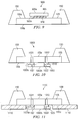
- FIGURE 9 is a cross-sectional view of integrated circuit device 900, which comprises IC die 105 and IC package 150 with auxiliary component 905 mounted on upper surface 105a of IC die 105 according to an exemplary embodiment of the present invention.
- Auxiliary component 905 comprises upper surface 905a and lower surface 905b.
- auxiliary component 905 may be, for example, an integrated circuit die having exposed test points on upper surface 905a and exposed circuit connection points on lower surface 905b.
- auxiliary component 905 may be a sensor element (e.g., capacitive chemical, micro-channel, etc.).
- Auxiliary component 905 is attached to IC die 105 by means of solder balls 910.
- Each solder ball 910 connects an exposed circuit connection point on lower surface 905b of auxiliary component 905 to a corresponding exposed circuit connection point on upper surface 105a of IC die 105.
- solder used in the form of solder balls
- other means of connection are also possible.
- FIGURE 10 is a cross-sectional view of integrated circuit device 1000, which comprises IC die 105 and IC package 150 with auxiliary component 1005 mounted on lower surface 105b of IC die 105 according to an exemplary embodiment of the present invention.
- Auxiliary component 1005 comprises upper surface 1005a and lower surface 1005b.
- auxiliary component 1005 may be, for example, an integrated circuit die having exposed test points on lower surface 1005b and exposed circuit connection points on upper surface 1005b.
- auxiliary component 1005 may be a sensor element (e.g., capacitive, chemical, micro-channel, etc.).
- IC die 105 has a plurality of vias, such as exemplary vias 1031 and 1032, passing through the silicon of IC die 105.
- auxiliary component 1005 has a plurality of vias, such as exemplary vias 1021 and 1022, passing through the body (silicon or other material) of auxiliary component 1005.
- Auxiliary component 1005 is attached to IC die 105 by means of raised metal contact pad 1010. Each metal contact pad 1010 connects an exposed circuit connection point on upper surface 1005a of auxiliary component 1005 to a corresponding exposed circuit connection point on lower surface 105b of IC die 105.
- auxiliary component 905 and auxiliary component 1005 may both be attached to opposite sides of IC die 105 at the same time. Also, the means of attachment may readily be modified so that either or both of auxiliary component 905 and auxiliary component 1005 may be removably attached, rather than permanently attached, to IC die 105.
- FIGURE 11 is a cross-sectional view of integrated circuit assembly 1100, which comprises IC die 105, IC package 150, and auxiliary component 1005 as illustrated in FIGURE 10, mounted on printed circuit board (PCB) 1110.
- An opening in printed circuit board 1110 is made to provide access to auxiliary component 1005 mounted on the lower surface of integrated circuit die 105.
- the lower surface of printed circuit board 1110 can be made in the same plane as the lower surface of auxiliary component 1005 in order to maintain a planar surface.
- an auxiliary component may be attached not only to an integrated circuit die containing active components, but may also be attached to an entirely passive electrical component, such as a sensor.
- the auxiliary component may be an active integrated circuit, a pre-packaged IC (such as a Quad Flat No-lead package), or a passive component, such as a resistor or a capacitor array.
- integrated circuit die 105 may be a sensor array and the auxiliary component may be an active integrated circuit.
Landscapes
- Engineering & Computer Science (AREA)
- Human Computer Interaction (AREA)
- Physics & Mathematics (AREA)
- General Physics & Mathematics (AREA)
- Multimedia (AREA)
- Theoretical Computer Science (AREA)
- Structures Or Materials For Encapsulating Or Coating Semiconductor Devices Or Solid State Devices (AREA)
- Credit Cards Or The Like (AREA)
Abstract
Description
Claims (15)
- An integrated circuit (IC) device comprising:an integrated circuit (IC) die having a first surface, a second surface opposite said first surface, and sidewalls extending between said first surface and said second surface;an integrated circuit (IC) package for supporting said IC die, wherein said IC package is attached to at least one of said sidewalls of said IC die such that at least a portion of said IC die first surface and at least a portion of said IC die second surface are exposed; andat least one auxiliary component attached to at least one of said exposed portion of said IC die first surface and said exposed portion of said IC die second surface.
- An electrical assembly comprising:a printed circuit board having a plurality of integrated circuit (IC) devices disposed on a first surface of said printed circuit board, at least one of said IC devices comprising:an integrated circuit (IC) die having a first surface, a second surface opposite said first surface, and sidewalls extending between said first surface and said second surface;an integrated circuit (IC) package for supporting said IC die, wherein said IC package is attached to at least one of said sidewalls of said IC die such that at least a portion of said IC die first surface and at least a portion of said IC die second surface are exposed; andat least one auxiliary component attached to at least one of said exposed portion of said IC die first surface and said exposed portion of said IC die second surface.
- The device or electrical assembly as set forth in any preceding Claim wherein said IC package encases at least one electrical connection extending between a contact pad on said peripheral portion of said IC die first surface and a contact pad disposed on said IC package second surface.
- The device or electrical assembly as set forth in Claim 3 wherein an exposed surface of said contact pad disposed on said IC package second surface lies in substantially the same plane as IC die second surface.
- The device or electrical assembly as set forth in Claim 3or 4 wherein an exposed surface of said contact pad disposed on said IC package second surface is recessed in an indentation in said IC package second surface.
- An integrated circuit (IC) device comprising:an integrated circuit (IC) die having a first surface, a second surface opposite said first surface, and sidewalls extending between said first surface and said second surface;an intermediate substrate having a first surface, a second surface opposite said first surface, and sidewalls extending between said first surface and said second surface, wherein said intermediate substrate second surface lies in substantially the same plane as said IC die second surface;an integrated circuit (IC) package for supporting said IC die and said intermediate substrate, wherein said IC package is attached to at least one IC die sidewall and at least one intermediate substrate sidewall, such that at least a portion of said IC die first surface and at least a portion of said IC die second surface are exposed and at least a portion of said intermediate substrate second surface is exposed; andat least one auxiliary component attached to at least one of said exposed portion of said IC die first surface and said exposed portion of said IC die second surface.
- The integrated circuit (IC) device or assembly as set forth in any preceding Claim wherein said IC package has a first surface and a second surface opposite said IC package first surface, and wherein said IC package second surface lies in substantially the same plane as said IC die second surface.
- The integrated circuit (IC) device or assembly as set forth in Claim 7 wherein a first portion of said IC package is attached to and covers at least part of a peripheral portion of said IC die first surface.
- The integrated circuit (IC) device as set forth in Claim 8 wherein said IC package encases at least one electrical connection extending between a contact pad on said peripheral portion of said IC die first surface and a contact pad disposed on said intermediate substrate second surface.
- The integrated circuit (IC) device as set forth in Claim 6 or any claim appended thereto wherein an exposed surface of said contact pad disposed on said intermediate substrate second surface lies in substantially the same plane as IC die second surface.
- The integrated circuit (IC) device as set forth in Claim 6 or any claims appended thereto wherein an exposed surface of said contact pad disposed on said intermediate substrate second surface is recessed in an indentation in said IC die second surface.
- The integrated circuit (IC) device or assembly as set forth in any preceding Claim wherein substantially all of said IC die second surface is exposed.
- The integrated circuit (IC) device or assembly as set forth in any preceding Claim wherein said at least one auxiliary component comprises a first auxiliary component having an exposed circuit connection point on a first surface of said first auxiliary component that is attached to at an exposed circuit connection point on said IC die first surface.
- The integrated circuit (IC) device or assembly as set forth in any preceding Claim said at least one auxiliary component comprises a second auxiliary component having an exposed circuit connection point on a first surface of said second auxiliary component that is attached to at an exposed circuit connection point on said IC die second surface.
- The integrated circuit (IC) device or assembly as set forth in any preceding Claim wherein said at least one auxiliary component is removably attached to said at least one of said exposed portion of said IC die first surface and said exposed portion of said IC die second surface.
Applications Claiming Priority (2)
| Application Number | Priority Date | Filing Date | Title |
|---|---|---|---|
| US400207 | 2003-03-27 | ||
| US10/400,207 US7109574B2 (en) | 2002-07-26 | 2003-03-27 | Integrated circuit package with exposed die surfaces and auxiliary attachment |
Publications (3)
| Publication Number | Publication Date |
|---|---|
| EP1465244A2 true EP1465244A2 (en) | 2004-10-06 |
| EP1465244A3 EP1465244A3 (en) | 2004-12-01 |
| EP1465244B1 EP1465244B1 (en) | 2013-12-04 |
Family
ID=32850543
Family Applications (1)
| Application Number | Title | Priority Date | Filing Date |
|---|---|---|---|
| EP04251766.4A Expired - Lifetime EP1465244B1 (en) | 2003-03-27 | 2004-03-26 | Integrated circuit package with exposed die surfaces and auxiliary attachment |
Country Status (3)
| Country | Link |
|---|---|
| US (1) | US7109574B2 (en) |
| EP (1) | EP1465244B1 (en) |
| JP (1) | JP4926380B2 (en) |
Cited By (2)
| Publication number | Priority date | Publication date | Assignee | Title |
|---|---|---|---|---|
| EP2154713A1 (en) * | 2008-08-11 | 2010-02-17 | Sensirion AG | Method for manufacturing a sensor device with a stress relief layer |
| EP2490250A1 (en) * | 2011-02-18 | 2012-08-22 | Robert Bosch GmbH | Mould module with sensor element |
Families Citing this family (35)
| Publication number | Priority date | Publication date | Assignee | Title |
|---|---|---|---|---|
| US6998721B2 (en) * | 2002-11-08 | 2006-02-14 | Stmicroelectronics, Inc. | Stacking and encapsulation of multiple interconnected integrated circuits |
| US20050093135A1 (en) * | 2003-10-31 | 2005-05-05 | Wei-Chi Liu | Thermal dissipating element of a chip |
| KR101172527B1 (en) * | 2005-03-31 | 2012-08-10 | 스태츠 칩팩, 엘티디. | Semiconductor stacked package assembly having exposed substrate surfaces on upper and lower sides |
| US7364945B2 (en) | 2005-03-31 | 2008-04-29 | Stats Chippac Ltd. | Method of mounting an integrated circuit package in an encapsulant cavity |
| US7354800B2 (en) * | 2005-04-29 | 2008-04-08 | Stats Chippac Ltd. | Method of fabricating a stacked integrated circuit package system |
| US7288757B2 (en) | 2005-09-01 | 2007-10-30 | Micron Technology, Inc. | Microelectronic imaging devices and associated methods for attaching transmissive elements |
| US7768125B2 (en) | 2006-01-04 | 2010-08-03 | Stats Chippac Ltd. | Multi-chip package system |
| US7456088B2 (en) | 2006-01-04 | 2008-11-25 | Stats Chippac Ltd. | Integrated circuit package system including stacked die |
| US7750482B2 (en) | 2006-02-09 | 2010-07-06 | Stats Chippac Ltd. | Integrated circuit package system including zero fillet resin |
| US7435619B2 (en) * | 2006-02-14 | 2008-10-14 | Stats Chippac Ltd. | Method of fabricating a 3-D package stacking system |
| US8704349B2 (en) | 2006-02-14 | 2014-04-22 | Stats Chippac Ltd. | Integrated circuit package system with exposed interconnects |
| JP4972968B2 (en) * | 2006-03-16 | 2012-07-11 | 富士通株式会社 | Semiconductor device and manufacturing method thereof |
| US7501697B2 (en) * | 2006-03-17 | 2009-03-10 | Stats Chippac Ltd. | Integrated circuit package system |
| US20070216033A1 (en) * | 2006-03-20 | 2007-09-20 | Corisis David J | Carrierless chip package for integrated circuit devices, and methods of making same |
| DE102006030581B3 (en) * | 2006-07-03 | 2008-02-21 | Infineon Technologies Ag | Method for producing a component |
| TWI313943B (en) * | 2006-10-24 | 2009-08-21 | Chipmos Technologies Inc | Light emitting chip package and manufacturing thereof |
| SG147330A1 (en) | 2007-04-19 | 2008-11-28 | Micron Technology Inc | Semiconductor workpiece carriers and methods for processing semiconductor workpieces |
| US8124451B2 (en) | 2007-09-21 | 2012-02-28 | Stats Chippac Ltd. | Integrated circuit packaging system with interposer |
| US8258015B2 (en) * | 2008-02-22 | 2012-09-04 | Stats Chippac Ltd. | Integrated circuit package system with penetrable film adhesive |
| US8304869B2 (en) * | 2008-08-01 | 2012-11-06 | Stats Chippac Ltd. | Fan-in interposer on lead frame for an integrated circuit package on package system |
| EP2192825A1 (en) * | 2008-11-26 | 2010-06-02 | Osram Gesellschaft mit Beschränkter Haftung | An injection tool for encapsulating electronic circuits with light sources, and related encapsulation process |
| EP2224218B1 (en) * | 2009-02-25 | 2018-11-28 | Sensirion Automotive Solutions AG | A sensor in a moulded package and a method for manufacturing the same |
| US8350381B2 (en) * | 2010-04-01 | 2013-01-08 | Infineon Technologies Ag | Device and method for manufacturing a device |
| US8273607B2 (en) * | 2010-06-18 | 2012-09-25 | Stats Chippac Ltd. | Integrated circuit packaging system with encapsulation and underfill and method of manufacture thereof |
| US8737080B2 (en) | 2011-01-14 | 2014-05-27 | Qualcomm Incorporated | Modular surface mount package for a system on a chip |
| EP2573804A1 (en) * | 2011-09-21 | 2013-03-27 | Nxp B.V. | Integrated circuit with sensor and manufacturing method thereof |
| EP2709143A1 (en) * | 2012-09-18 | 2014-03-19 | Gemalto SA | Moulding method for manufacturing an electronic package |
| US9269597B2 (en) * | 2013-01-23 | 2016-02-23 | Microchip Technology Incorporated | Open cavity plastic package |
| CN104051367A (en) * | 2014-07-01 | 2014-09-17 | 苏州晶方半导体科技股份有限公司 | Packaging structure and packaging method for fingerprint recognition chip |
| JP6231459B2 (en) * | 2014-10-29 | 2017-11-15 | アオイ電子株式会社 | Manufacturing method of semiconductor device |
| US20160360622A1 (en) * | 2015-06-02 | 2016-12-08 | Microchip Technology Incorporated | Integrated Circuit With Sensor Printed In Situ |
| KR20170082358A (en) * | 2016-01-06 | 2017-07-14 | 하나 마이크론(주) | Device for track pad semiconductor package of smart phone and method for manufacturing the same |
| TWI672779B (en) * | 2016-12-28 | 2019-09-21 | 曦威科技股份有限公司 | Fingerprint identification device, mobile device using the same and method for manufacturing fingerprint identification device |
| CN112549431B (en) * | 2020-11-13 | 2023-07-21 | 深圳先进技术研究院 | A method for preparing a nested structure used in a liquid generating device |
| CN112571718B (en) * | 2020-11-13 | 2023-06-20 | 深圳先进技术研究院 | A preparation method of a nested structure of a microchannel array plate and a droplet generating device |
Family Cites Families (22)
| Publication number | Priority date | Publication date | Assignee | Title |
|---|---|---|---|---|
| US5604376A (en) * | 1994-06-30 | 1997-02-18 | Digital Equipment Corporation | Paddleless molded plastic semiconductor chip package |
| JP3207738B2 (en) * | 1996-01-15 | 2001-09-10 | 株式会社東芝 | Resin-sealed semiconductor device and method of manufacturing the same |
| JP4024335B2 (en) * | 1996-01-26 | 2007-12-19 | ハリス コーポレイション | Integrated circuit device having an opening exposing die of integrated circuit and manufacturing method thereof |
| US5891753A (en) * | 1997-01-24 | 1999-04-06 | Micron Technology, Inc. | Method and apparatus for packaging flip chip bare die on printed circuit boards |
| GB9725571D0 (en) * | 1997-12-04 | 1998-02-04 | Philips Electronics Nv | Electronic apparatus comprising fingerprint sensing devices |
| US6091082A (en) * | 1998-02-17 | 2000-07-18 | Stmicroelectronics, Inc. | Electrostatic discharge protection for integrated circuit sensor passivation |
| US6117797A (en) * | 1998-09-03 | 2000-09-12 | Micron Technology, Inc. | Attachment method for heat sinks and devices involving removal of misplaced encapsulant |
| US6429530B1 (en) * | 1998-11-02 | 2002-08-06 | International Business Machines Corporation | Miniaturized chip scale ball grid array semiconductor package |
| US6242932B1 (en) * | 1999-02-19 | 2001-06-05 | Micron Technology, Inc. | Interposer for semiconductor components having contact balls |
| EP1041628A3 (en) * | 1999-03-29 | 2008-05-28 | Interuniversitair Microelektronica Centrum Vzw | An image sensor ball grid array package and the fabrication thereof |
| JP2001056204A (en) * | 1999-08-19 | 2001-02-27 | Sony Corp | Capacitive fingerprint sensor |
| JP2001196505A (en) * | 1999-11-05 | 2001-07-19 | Sony Corp | Semiconductor chip surface exposed type resin-encapsulated semiconductor package |
| JP2001185657A (en) * | 1999-12-10 | 2001-07-06 | Amkor Technology Korea Inc | Semiconductor package and manufacturing method thereof |
| JP2001185651A (en) * | 1999-12-27 | 2001-07-06 | Matsushita Electronics Industry Corp | Semiconductor device and method of manufacturing the same |
| JP2001332573A (en) * | 2000-05-22 | 2001-11-30 | Sony Corp | Resin sealing mold, method of manufacturing semiconductor device, and semiconductor device |
| US6342406B1 (en) * | 2000-11-15 | 2002-01-29 | Amkor Technology, Inc. | Flip chip on glass image sensor package fabrication method |
| JP4422323B2 (en) * | 2000-12-15 | 2010-02-24 | 株式会社ルネサステクノロジ | Semiconductor device |
| JP2002261194A (en) * | 2001-02-28 | 2002-09-13 | Mitsumi Electric Co Ltd | Semiconductor device |
| JP2002261232A (en) * | 2001-03-01 | 2002-09-13 | Hitachi Ltd | Semiconductor device |
| JP4418120B2 (en) * | 2001-03-12 | 2010-02-17 | グローリー株式会社 | Fingerprint sensor, fingerprint collation device, and method of manufacturing fingerprint sensor |
| JP3650596B2 (en) * | 2001-09-03 | 2005-05-18 | 新光電気工業株式会社 | Manufacturing method of semiconductor device |
| US6534859B1 (en) * | 2002-04-05 | 2003-03-18 | St. Assembly Test Services Ltd. | Semiconductor package having heat sink attached to pre-molded cavities and method for creating the package |
-
2003
- 2003-03-27 US US10/400,207 patent/US7109574B2/en not_active Expired - Lifetime
-
2004
- 2004-03-26 JP JP2004093393A patent/JP4926380B2/en not_active Expired - Lifetime
- 2004-03-26 EP EP04251766.4A patent/EP1465244B1/en not_active Expired - Lifetime
Cited By (4)
| Publication number | Priority date | Publication date | Assignee | Title |
|---|---|---|---|---|
| EP2154713A1 (en) * | 2008-08-11 | 2010-02-17 | Sensirion AG | Method for manufacturing a sensor device with a stress relief layer |
| EP2154714A3 (en) * | 2008-08-11 | 2010-03-24 | Sensirion AG | Temperature sensor with buffer layer |
| US7901971B2 (en) | 2008-08-11 | 2011-03-08 | Sensirion Ag | Method for manufacturing a sensor device with a stress relief layer |
| EP2490250A1 (en) * | 2011-02-18 | 2012-08-22 | Robert Bosch GmbH | Mould module with sensor element |
Also Published As
| Publication number | Publication date |
|---|---|
| EP1465244A3 (en) | 2004-12-01 |
| JP2004297071A (en) | 2004-10-21 |
| US20040017000A1 (en) | 2004-01-29 |
| EP1465244B1 (en) | 2013-12-04 |
| JP4926380B2 (en) | 2012-05-09 |
| US7109574B2 (en) | 2006-09-19 |
Similar Documents
| Publication | Publication Date | Title |
|---|---|---|
| US7109574B2 (en) | Integrated circuit package with exposed die surfaces and auxiliary attachment | |
| US7989938B2 (en) | Semiconductor device for fingerprint recognition | |
| EP1811566B1 (en) | Three-dimensional Multi-Chips and tri-axial sensors and methods of manufacuring the same | |
| US6900531B2 (en) | Image sensor device | |
| TW536522B (en) | Hermetic MEMS package with interlocking layers | |
| US20030002265A1 (en) | Mems package with flexible circuit interconnect | |
| US7319598B2 (en) | Electronic component with a housing package | |
| US20080157298A1 (en) | Stress Mitigation in Packaged Microchips | |
| EP2948979B1 (en) | Open cavity plastic package | |
| US6888238B1 (en) | Low warpage flip chip package solution-channel heat spreader | |
| US6700190B2 (en) | Integrated circuit device with exposed upper and lower die surfaces | |
| US20090079052A1 (en) | Semiconductor package, apparatus and method for manufacturing the semiconductor package, and electronic device equipped with the semiconductor package | |
| CN101337652A (en) | Packaging of sensor element contact surfaces and packaging method thereof | |
| US20080009096A1 (en) | Package-on-package and method of fabricating the same | |
| US20100078804A1 (en) | Apparatus with Side Mounted Microchip | |
| EP2884242B1 (en) | Sensor Package And Manufacturing Method | |
| US20080164619A1 (en) | Semiconductor chip package and method of manufacturing the same | |
| JPH04370957A (en) | Multichip package | |
| KR100663549B1 (en) | Semiconductor package and manufacturing method | |
| KR20080068299A (en) | Semiconductor module and manufacturing method | |
| JP2006129448A (en) | Communication module | |
| KR20090122771A (en) | Semiconductor package and manufacturing method thereof | |
| US12198995B2 (en) | Covers for semiconductor package components | |
| TWI399974B (en) | Camera module assembly method | |
| CN1998078A (en) | Single row bonding pad structure of integrated circuit chip |
Legal Events
| Date | Code | Title | Description |
|---|---|---|---|
| PUAI | Public reference made under article 153(3) epc to a published international application that has entered the european phase |
Free format text: ORIGINAL CODE: 0009012 |
|
| AK | Designated contracting states |
Kind code of ref document: A2 Designated state(s): AT BE BG CH CY CZ DE DK EE ES FI FR GB GR HU IE IT LI LU MC NL PL PT RO SE SI SK TR |
|
| AX | Request for extension of the european patent |
Extension state: AL HR LT LV MK |
|
| PUAL | Search report despatched |
Free format text: ORIGINAL CODE: 0009013 |
|
| AK | Designated contracting states |
Kind code of ref document: A3 Designated state(s): AT BE BG CH CY CZ DE DK EE ES FI FR GB GR HU IE IT LI LU MC NL PL PT RO SE SI SK TR |
|
| AX | Request for extension of the european patent |
Extension state: AL HR LT LV MK |
|
| RIC1 | Information provided on ipc code assigned before grant |
Ipc: 7H 01L 23/31 B Ipc: 7H 01L 21/56 A Ipc: 7G 06K 9/20 B Ipc: 7G 06T 1/00 B |
|
| 17P | Request for examination filed |
Effective date: 20050520 |
|
| AKX | Designation fees paid |
Designated state(s): DE FR GB IT |
|
| RAP1 | Party data changed (applicant data changed or rights of an application transferred) |
Owner name: STMICROELECTRONICS, INC. |
|
| RIC1 | Information provided on ipc code assigned before grant |
Ipc: G06T 1/00 20060101ALI20130705BHEP Ipc: G06K 9/00 20060101ALI20130705BHEP Ipc: G06K 9/20 20060101ALI20130705BHEP Ipc: H01L 23/00 20060101ALI20130705BHEP Ipc: H01L 21/56 20060101AFI20130705BHEP Ipc: H01L 23/31 20060101ALI20130705BHEP |
|
| GRAP | Despatch of communication of intention to grant a patent |
Free format text: ORIGINAL CODE: EPIDOSNIGR1 |
|
| INTG | Intention to grant announced |
Effective date: 20130813 |
|
| INTG | Intention to grant announced |
Effective date: 20130821 |
|
| GRAS | Grant fee paid |
Free format text: ORIGINAL CODE: EPIDOSNIGR3 |
|
| GRAA | (expected) grant |
Free format text: ORIGINAL CODE: 0009210 |
|
| AK | Designated contracting states |
Kind code of ref document: B1 Designated state(s): DE FR GB IT |
|
| REG | Reference to a national code |
Ref country code: GB Ref legal event code: FG4D |
|
| REG | Reference to a national code |
Ref country code: DE Ref legal event code: R096 Ref document number: 602004043923 Country of ref document: DE Effective date: 20140130 |
|
| REG | Reference to a national code |
Ref country code: DE Ref legal event code: R097 Ref document number: 602004043923 Country of ref document: DE |
|
| PLBE | No opposition filed within time limit |
Free format text: ORIGINAL CODE: 0009261 |
|
| STAA | Information on the status of an ep patent application or granted ep patent |
Free format text: STATUS: NO OPPOSITION FILED WITHIN TIME LIMIT |
|
| 26N | No opposition filed |
Effective date: 20140905 |
|
| GBPC | Gb: european patent ceased through non-payment of renewal fee |
Effective date: 20140326 |
|
| REG | Reference to a national code |
Ref country code: DE Ref legal event code: R097 Ref document number: 602004043923 Country of ref document: DE Effective date: 20140905 |
|
| PG25 | Lapsed in a contracting state [announced via postgrant information from national office to epo] |
Ref country code: GB Free format text: LAPSE BECAUSE OF NON-PAYMENT OF DUE FEES Effective date: 20140326 |
|
| PG25 | Lapsed in a contracting state [announced via postgrant information from national office to epo] |
Ref country code: IT Free format text: LAPSE BECAUSE OF FAILURE TO SUBMIT A TRANSLATION OF THE DESCRIPTION OR TO PAY THE FEE WITHIN THE PRESCRIBED TIME-LIMIT Effective date: 20131204 |
|
| REG | Reference to a national code |
Ref country code: FR Ref legal event code: PLFP Year of fee payment: 13 |
|
| REG | Reference to a national code |
Ref country code: FR Ref legal event code: PLFP Year of fee payment: 14 |
|
| REG | Reference to a national code |
Ref country code: FR Ref legal event code: PLFP Year of fee payment: 15 |
|
| REG | Reference to a national code |
Ref country code: DE Ref legal event code: R082 Ref document number: 602004043923 Country of ref document: DE Representative=s name: PAGE, WHITE & FARRER GERMANY LLP, DE |
|
| PGFP | Annual fee paid to national office [announced via postgrant information from national office to epo] |
Ref country code: FR Payment date: 20230222 Year of fee payment: 20 |
|
| PGFP | Annual fee paid to national office [announced via postgrant information from national office to epo] |
Ref country code: DE Payment date: 20230221 Year of fee payment: 20 |
|
| REG | Reference to a national code |
Ref country code: DE Ref legal event code: R071 Ref document number: 602004043923 Country of ref document: DE |