EP1465086A2 - Integrated circuit design system and method using preprocessor which changes hardware description in accordance with configuration - Google Patents
Integrated circuit design system and method using preprocessor which changes hardware description in accordance with configuration Download PDFInfo
- Publication number
- EP1465086A2 EP1465086A2 EP03013454A EP03013454A EP1465086A2 EP 1465086 A2 EP1465086 A2 EP 1465086A2 EP 03013454 A EP03013454 A EP 03013454A EP 03013454 A EP03013454 A EP 03013454A EP 1465086 A2 EP1465086 A2 EP 1465086A2
- Authority
- EP
- European Patent Office
- Prior art keywords
- description
- circuit
- file
- flip
- flop
- Prior art date
- Legal status (The legal status is an assumption and is not a legal conclusion. Google has not performed a legal analysis and makes no representation as to the accuracy of the status listed.)
- Withdrawn
Links
Images






Classifications
-
- G—PHYSICS
- G06—COMPUTING OR CALCULATING; COUNTING
- G06F—ELECTRIC DIGITAL DATA PROCESSING
- G06F30/00—Computer-aided design [CAD]
- G06F30/30—Circuit design
Definitions
- the present invention relates to a preprocessor which is used to automate operation of changing a hardware description in accordance with a configuration.
- the present invention also relates to an integrated circuit design system using the preprocessor and an integrated circuit design method by the system.
- the present invention is particularly suitable for a system which automatically creates IP and software IP in accordance with user's designation, which creates a circuit description file which can designate synchronous/asynchronous reset of a flip-flop or change the cluster combination of a gated clock.
- an integrated circuit design system is designed to have an arrangement as shown in FIG. 1.
- a computer system used to design such an integrated circuit and a method thereof are described in, e.g., U.S. Patent No. 5,987,239 issued to Graham Kirsch, "COMPUTER SYSTEM AND METHOD FOR BUILDING A HARDWARE DESCRIPTION LANGUAGE REPRESENTATION OF CONTROL LOGIC FOR A COMPLEX DIGITAL SYSTEM", Nov. 16, 1999.
- a circuit description file 11 which is described by a user using an existing language (Verilog-HDL: Verilog-Hardware Description Language or VHDL: Very high speed integrated circuits Hardware Description Language) and a logic synthesis control script file 12 (script file which controls a logic synthesis program) are logically synthesized by a logic synthesis program 14 of a processor (logic synthesis tool or computer) 13.
- the logic synthesis program 14 executes processing for converting the circuit description file 11 into a circuit description file using a "cell" serving as a basic unit of a circuit to create a netlist 15.
- the netlist 15 is processed by a layout wiring program (a program which lays out cells and wirings) 16 to determine the layout of the cells and wirings so that the circuit of a chip (semiconductor integrated circuit) 17 is designed.
- a tool which automatically inserts a circuit for gated clock formation already exists (e.g., Marcus Blüml et al., "A Workbench for Generation of Component Models", 0-8186-4350-1/93 1993 IEEE, pp. 466-471).
- this tool cannot meet a particular requirement to, e.g., combine designated clusters and is not necessarily satisfactory.
- a preprocessor which processes a first circuit description file containing a first hardware description language and a second hardware description language on the basis of a preprocessor control file, and converts at least a portion described by the first hardware description language in the first circuit description file into the second hardware description language to create and output a second circuit description file.
- a circuit description file (second circuit description file) capable of changing the synchronous/ asynchronous designation of a flip-flop or the cluster combination of gated clock can be created without intervening manual operation.
- the manual operation time can be shortened, bugs can be prevented, and no time is required for verification operation.
- an integrated circuit design system comprising a preprocessor which processes a first circuit description file containing a description of a flip-flop described by a first hardware description language on the basis of a preprocessor control file, creates a second circuit description file by converting at least the description of the flip-flop into a second hardware description language, and creates a logic synthesis control script file for a gated clock circuit, and a logic synthesis tool which subjects the second circuit description file logical synthesizes using logic synthesis control script file created by the preprocessor and converts the files into a circuit description file using a cell as a basic unit of a circuit to create a netlist and determines a layout of cells and wirings in an integrated circuit on the basis of the netlist.
- the preprocessor creates a circuit description file (second circuit description file) capable of changing the synchronous/asynchronous designation of a flip-flop or the cluster combination of gated clock.
- An integrated circuit can be designed while automating processing that is conventionally executed by manual operation. Accordingly, the operation time can be shortened, bugs due to manual operation can be prevented, and no time is required for verification operation. Hence, the development period of integrated circuits can be shortened, and the cost for design can also be reduced.
- an integrated circuit design method comprising steps of inputting, to a preprocessor, a circuit description file containing a first hardware description language and a second hardware description language and a preprocessor control file which controls operation of the preprocessor and converting at least a portion described by the first hardware description language in the circuit description file into the second hardware description language, logically synthesizing a circuit description file output from the preprocessor using a logic synthesis control script file for a gated clock circuit and a logic synthesis control script file for circuits other than the gated clock circuit by a logic synthesis tool to convert the files into a circuit description file using a cell as a basic unit of a circuit and create a netlist, and determining the layout of the cells and wirings on the basis of the netlist to design a circuit of a chip.
- an integrated circuit can be designed while automating processing that is conventionally executed by manual operation. Accordingly, the operation time can be shortened, bugs due to manual operation can be prevented, and no time is required for verification operation. As a result, the development period of integrated circuits can be shortened, and the cost for design can be reduced.
- FIG. 2 is a functional block diagram for explaining a preprocessor and integrated circuit design system according to the embodiment of the present invention, which shows the schematic arrangement of the entire system.
- a circuit description file 21 described by a user and a preprocessor control file 22 (a description file which controls the operation of the preprocessor) that is also described by the user are input to a preprocessor 23. Processing for the circuit description file 21 is executed on the basis of the control data of the preprocessor control file 22.
- the circuit description file 21 contains different hardware description languages (to be referred to as a description language A and description language B herein).
- the circuit description file 21 also has pieces of information (a) to (f) described.
- the description language A in the circuit description file 21 is converted into the existing description language B (Verilog-HDL or VHDL) by the preprocessor 23 to generate a circuit description file 24.
- a logic synthesis program 25 generates a logic synthesis control script file (for gated clock circuit) 26 to be used for gated clock formation.
- a logic synthesis script file 28 which is prepared in advance for control of circuits other than gated clocks is input to a logic synthesis tool (computer) 27.
- a logic synthesis program 25 processing for converting the circuit description file 24 into a circuit description file using a cell as a basic unit of a circuit is executed. At this time, how to lay out cells and wirings is not determined yet.
- a netlist (a circuit description using cells output from the logic synthesis program) 29 is created by the logic synthesis program 25.
- the netlist 29 is processed by a layout wiring program (a program which lays out cells and wirings) 30 so the layout of cells and wirings is determined.
- a layout wiring program a program which lays out cells and wirings
- the circuit of a chip (semiconductor integrated circuit) 31 is designed.
- FIGS. 3 to 8 are flow charts showing the operation of the preprocessor 23 in the integrated circuit design system shown in FIG. 2.
- FIG. 3 is a flow chart showing the schematic operation of the preprocessor in the system shown in FIG. 2.
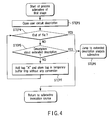
- FIG. 4 is a flow chart showing the process subroutine.
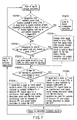
- FIG. 5 is a flow chart showing the extended description analysis subroutine.
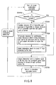
- FIG. 6 is a flow chart showing the process subroutine of the second stage.
- FIG. 7 is a flow chart showing the process subroutine of a tag B.
- FIG. 8 is a flow chart showing the cluster combination subroutine.
- the flow advances to the process subroutine of the first stage shown in FIG. 4 (STEP2).
- the circuit description file 21 by the user is opened (STEP3), and it is determined whether the file is ended (STEP4). If NO in STEP4, it is determined whether the file has a description about an extended description (STEP5). If YES in STEP5, the flow jumps to the extended description analysis subroutine (STEP6). If NO in STEP5, a tag "A" is added and stored in a temporary buffer tmp without any conversion (STEP7). Then, the flow returns to the determination operation in STEP4. The operation in STEP4 to STEP7 is repeated until it is determined that the file is ended. If YES in STEP4, the flow returns to the subroutine invocation source (STEP2).
- the extended description subroutine it is determined whether it is an extended description about a flip-flop (STEP8), as shown in FIG. 5. If YES in STEP8, pieces of information are stored in the variables of a structure FF by syntax analysis of the extended circuit description (STEP9). If NO in STEP8, error processing is executed, and the program is ended (STEP10).
- the name of the flip-flop is stored in Name.
- the number of bits of the flip-flop is stored in BitNum.
- the cluster number is stored in ClusterNo.
- the pointer to the name of control signal group of the flip-flop is stored in CtrlNamePtr * .
- a value which should be substituted when the number of control signals of the flip-flop becomes 1 or information of the pointer to the signal group is stored in ValPtr*.
- the tag "B” is added to the pointer of the entity of the structure FF and stored in the temporary buffer tmp (STEP11).
- the flow jumps to the process subroutine of the second stage (STEP12).
- the process subroutine of the second stage it is determined first whether the temporary buffer tmp is ended (STEP13), as shown in FIG. 6. If NO in STEP13, the tag and stored information are acquired from the temporary buffer tmp (STEP14). It is determined whether the tag is the tag "B" (STEP15). If NO in STEP15, the stored information is directly output to an output file OUT (STEP16). The flow returns to STEP13 to repeat the same processing as described above. If YES in STEP13, the flow returns to the subroutine invocation source (STEP12). On the other hand, if YES in STEP15, the flow jumps to the process subroutine of the tag "B" (STEP17).
- the clock signal stored in the array CTRL is changed such that a signal name after passing through a gated clock control circuit is used as a clock signal for a flip-flop.
- a Verilog description for the control circuit is output to the output file OUT (STEP21). If NO in STEP20, the clock signal stored in the array CTRL is used as a clock signal for a flip-flop (STEP22).
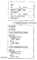
- FIG. 9 shows an input file and output file when the synchronous/asynchronous reset designation of a flip-flop is changed by the preprocessor shown in FIGS. 3 to 8.
- FIG. 9 shows output results of a conversion program A (Program A) when synchronous reset/asynchronous reset is set as the reset scheme of the flip-flop.
- ⁇ / and “/>” are markers.
- the description of a portion sandwiched between “ ⁇ /” and “/>” is a conversion object.
- clk clock designates the name (clock in this example) of a clock signal in the hardware description after conversion
- delay designates the delay value (2 in this example) of simulation in the hardware description after conversion.
- program A means the conversion program A of the preprocessor 23, option-SYNC designates to output, to program A, a hardware description which initializes the flip-flop by a synchronous reset scheme, and option-ASYNC designates to output, to program A, a hardware description which initializes the flip-flop by an asynchronous reset scheme.
- a processing result by the conversion program A is output in accordance with the synchronous/ asynchronous reset designation of the flip-flop.
- a circuit description file which can freely change the synchronous/asynchronous designation of a flip-flop can be created by the preprocessor 23.
- two descriptions about reset of the flip-flop i.e., a description with "synchronous reset” and a description with "asynchronous reset” can be obtained by executing the conversion program A twice.
- the description with "synchronous reset” and description with “asynchronous reset” can be obtained in a shorter time as compared to the case wherein the two descriptions are manually generated.
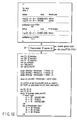
- FIG. 10 shows an example of an input file and output file of the preprocessor (conversion program A) 23 when the gated clock function is used without any grouping designation (when the cluster combination function is not used).
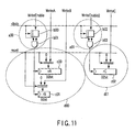
- FIG. 11 shows an example of a circuit formed from the output file shown in FIG. 10. Referring to FIG. 11, a00 and a01 represent circuits which stop (gating) a clock signal, b00 and b02 represent latches, b01 and b03 represent AND circuits, c00, c01, and c02 represent flip-flops, and d00 and d01 represent clusters.
- FIG. 12 shows an example of an input file and output file of the preprocessor (conversion program A) when the gated clock function is used with a grouping designation (when the cluster combination function is used).
- FIG. 13 shows an example of a circuit formed from the output file shown in FIG. 12. The signal enable gate-clock which instructs the gated clock function and a signal grouping ⁇ FF00, FF01 ⁇ which instructs the cluster combination function are input to the preprocessor 23.
- a00 represents a circuit which stops (gating) a clock signal
- b00 represents a latch
- b01 represents an AND circuit
- c00, c01, and c02 represent flip-flops
- d00 represents a cluster.
- the hardware description of a flip-flop is made in a format that does not specify whether the flip-flop is with synchronous reset or a flip-flop with an asynchronous reset.
- the description about the flip-flop is made using the first hardware description language in a file (first circuit description file) described using an existing hardware description language (second hardware description language).
- first circuit description file first circuit description file
- second hardware description language second hardware description language
- the description part about the flip-flop is converted into the existing hardware description language and output.
- a flip-flop description of synchronous reset scheme can be output in accordance with an argument supplied to the conversion program A.
- a flip-flop description of asynchronous reset scheme can also be output.
- a designation to use a gated clock as the clock of the flip-flop can be designated for the conversion program A.
- a description with clock gating of the flip-flop is created.
- a clock can be shared by the descriptions X and Y, and gated clock formation can be executed for the shared clock (cluster combination).
- a circuit description file which can change the synchronous/asynchronous designation of a flip-flop and the cluster combination of a gated clock can be created by the preprocessor 23. For this reason, the development period can be shortened, and the cost can be reduced. In manual operation, correction must be performed because of bugs, and function verification operation must be executed every time a circuit is corrected. With the automation, the verification operation is unnecessary. The development period can be shortened, and the cost can be reduced even from this viewpoint.
- circuit description file 21 and preprocessor control file 22 have been described as separate files for the descriptive convenience. However, the files may be integrated into one file, as a matter of course.
- a preprocessor which can create a circuit description file capable of changing the synchronous/asynchronous designation of a flip-flop and the cluster combination of gated clock can be obtained.
Landscapes
- Engineering & Computer Science (AREA)
- Computer Hardware Design (AREA)
- Physics & Mathematics (AREA)
- Theoretical Computer Science (AREA)
- Evolutionary Computation (AREA)
- Geometry (AREA)
- General Engineering & Computer Science (AREA)
- General Physics & Mathematics (AREA)
- Design And Manufacture Of Integrated Circuits (AREA)
Abstract
Description
Claims (20)
- A preprocessor which changes a hardware description in accordance with a configuration, characterized in that
a first circuit description file (21) containing a first hardware description language and a second hardware description language is processed on the basis of a preprocessor control file (22), and at least a portion described by the first hardware description language in the first circuit description file (21) is converted into the second hardware description language to create and output a second circuit description file (24). - A preprocessor according to claim 1, characterized in that a logic synthesis control script file (26) for a gated clock circuit is further created and output on the basis of the preprocessor control file (22) and the first circuit description file (21).
- A preprocessor according to claim 1, characterized in that the second hardware description language includes one of Verilog-HDL and VHDL.
- A preprocessor according to claim 1, characterized in that the processing of the first circuit description file (21) is processing of extracting the first hardware description language from the first circuit description file (21), converting the first hardware description language into the second hardware description language, and outputting the second circuit description file without converting a portion described by the second hardware description language in the first circuit description file (21).
- A preprocessor according to claim 1, characterized in that the first circuit description file (21) includes a description about a flip-flop, which is described by the first hardware description language, and information corresponding to a circuit obtained by forming a gated clock of the description about the flip-flop is converted into the second hardware description language and output.
- A preprocessor according to claim 5, characterized in that the description about the flip-flop, which is made by the first hardware description language, is made without specifying a reset scheme of the flip-flop, and whether the flip-flop should use a synchronous reset scheme or an asynchronous reset scheme is designated in converting at least the portion described by the first hardware description language in the first circuit description file (21) into the second hardware description language.
- A preprocessor according to claim 5, characterized in that in the description about the flip-flop, one cluster number is assigned to one flip-flop description.
- A preprocessor according to claim 5, characterized in that the second circuit description file (24) is obtained by converting descriptions of flip-flops indicated by a plurality of cluster numbers into a description of a flip-flop to be driven by one gated clock signal.
- An integrated circuit design system having a logic synthesis tool which determines a layout of cells and wirings in an integrated circuit on the basis of a netlist, characterized by comprising:wherein the second circuit description file (24) to logical synthesizes using logic synthesis control script file (26) created by the preprocessor (23) and converted into a circuit description file using a cell as a basic unit of a circuit to create a netlist (29) and determine the layout of the cells and wirings in the integrated circuit.a preprocessor (23) which processes a first circuit description file (21) containing a description of a flip-flop described by a first hardware description language on the basis of a preprocessor control file (22), creates a second circuit description file (24) by converting at least the description of the flip-flop into a second hardware description language, and creates a logic synthesis control script file (26) for a gated clock circuit,
- A system according to claim 9, characterized in that the netlist (29) is created by logically synthesizing, in addition to the second circuit description file (24) and logic synthesis control script file (26), a logic synthesis control script file (28) for control other than a gated clock.
- A system according to claim 9, characterized in that information for gated clock formation of the flip-flop is created by logic synthesis by a logic synthesis tool (27).
- A system according to claim 9, characterized in that the description about the flip-flop, which is made by the first hardware description language, is made without specifying a reset scheme of the flip-flop, and whether the flip-flop should use a synchronous reset scheme or an asynchronous reset scheme is designated in converting at least the portion described by the first hardware description language in the first circuit description file into the second hardware description language.
- A system according to claim 9, characterized in that in the description about the flip-flop, one cluster number is assigned to one flip-flop description.
- A system according to claim 9, characterized in that the second circuit description file (24) is obtained by converting descriptions of flip-flops indicated by a plurality of cluster numbers into a description of a flip-flop to be driven by one gated clock signal.
- An integrated circuit design method which processes a netlist by a layout wiring program to determine a layout of cells and wirings in an integrated circuit, characterized by comprising steps of:inputting, to a preprocessor (23), a circuit description file (21) containing a first hardware description language and a second hardware.description language and a preprocessor control file which controls operation of the preprocessor and converting at least a portion described by the first hardware description language in the circuit description file (21) into the second hardware description language;logically synthesizing a circuit description file (24) output from the preprocessor (23) using a logic synthesis control script file (26) for a gated clock circuit and a logic synthesis control script file (28) for circuits other than the gated clock circuit by a logic synthesis tool (27) to convert the files into a circuit description file using a cell as a basic unit of a circuit and create a netlist (29); anddetermining the layout of the cells and the wirings on the basis of the netlist (29) to design a circuit of a chip.
- A method according to claim 15, characterized in that the circuit description file (21) includes a description about a flip-flop, which is made by the first hardware description language, and a synchronous/ asynchronous designation and cluster combination of a gated clock are changed by the preprocessor (23).
- A method according to claim 16, characterized in that the preprocessor control file (22) contains at least one of pieces of information representing a name of a reset signal, a name of a clock signal, a flip-flop reset scheme, whether a gated clock is to be formed, if the gated clock is to be formed, whether a description of clock gating is to be created by the preprocessor (23), whether the description is to be output in a description format that can be automatically recognized by an automatic gated clock formation function of a logic synthesis program (25), and information about clusters to be regarded as one.
- A method according to claim 15, characterized in that the step of converting at least the portion described by the first hardware description language in the circuit description file (21) into the second hardware description language comprises steps of
loading and interpreting the preprocessor control file (22) and storing the interpreted information in the preprocessor (23) (STEP1),
determining whether the information stored in the preprocessor (23) is related to an extended description (STEP5), and if the information is related to the extended description, analyzing the extended description (STEP8, STEP9, STEP11),
determining a tag when it is determined that the information is not related to the extended description (STEP14, STEP15, STEP16),
determining a cluster combination designation when it is determined that the tag is a predetermined tag (STEP27, STEP28, STEP29, STEP30),
designating whether the flip-flop should use synchronous reset or asynchronous reset (STEP23) and creating a circuit description corresponding to the flip-flop of synchronous reset (STEP25) or a circuit description corresponding to the flip-flop of asynchronous reset (STEP24), and
creating information necessary for cluster combination when the cluster combination designation is present (STEP27, STEP28). - A method according to claim 18, characterized in that the step of analyzing the extended description comprises steps of
determining whether the extended description is an extended description about the flip-flop (STEP8),
storing information in each variable of a structure flip-flop when it is determined in the determination step that the extended description is the extended description about the flip-flop (STEP9), and
adding a tag to a pointer to an entity of the structure flip-flop and storing the tag in a temporary buffer (STEP11). - A method according to claim 18, characterized in that the step of determining the tag comprises steps of
acquiring the tag and stored information from the temporary buffer (STEP14), and
determining whether the tag is the predetermined tag (STEP15), and when the tag is not the predetermined tag, directly outputting the stored information to an output file (STEP16).
Applications Claiming Priority (2)
| Application Number | Priority Date | Filing Date | Title |
|---|---|---|---|
| JP2003096687A JP3923920B2 (en) | 2003-03-31 | 2003-03-31 | Integrated circuit design system and integrated circuit design method |
| JP2003096687 | 2003-03-31 |
Publications (2)
| Publication Number | Publication Date |
|---|---|
| EP1465086A2 true EP1465086A2 (en) | 2004-10-06 |
| EP1465086A3 EP1465086A3 (en) | 2005-05-18 |
Family
ID=32844651
Family Applications (1)
| Application Number | Title | Priority Date | Filing Date |
|---|---|---|---|
| EP03013454A Withdrawn EP1465086A3 (en) | 2003-03-31 | 2003-06-24 | Integrated circuit design system and method using preprocessor which changes hardware description in accordance with configuration |
Country Status (4)
| Country | Link |
|---|---|
| US (1) | US6990641B2 (en) |
| EP (1) | EP1465086A3 (en) |
| JP (1) | JP3923920B2 (en) |
| TW (1) | TWI279698B (en) |
Families Citing this family (11)
| Publication number | Priority date | Publication date | Assignee | Title |
|---|---|---|---|---|
| EP2030135A2 (en) | 2006-05-22 | 2009-03-04 | Coherent Logix Incorporated | Designing an asic based on execution of a software program on a processing system |
| US8065640B1 (en) * | 2006-06-02 | 2011-11-22 | Cadence Design Systems, Inc. | Systems and methods for reduced test case generation |
| US8127113B1 (en) * | 2006-12-01 | 2012-02-28 | Synopsys, Inc. | Generating hardware accelerators and processor offloads |
| JP4955484B2 (en) * | 2007-08-24 | 2012-06-20 | ルネサスエレクトロニクス株式会社 | Circuit design apparatus, circuit design method, and circuit design program |
| EP2628090B1 (en) | 2010-10-15 | 2018-05-30 | Coherent Logix Incorporated | Disabling communication in a multiprocessor system |
| TW201301135A (en) * | 2011-06-16 | 2013-01-01 | Hon Hai Prec Ind Co Ltd | System and method for converting component data |
| US8954307B1 (en) * | 2011-10-10 | 2015-02-10 | Cadence Design Systems, Inc. | Chained programming language preprocessors for circuit simulation |
| CN102693340B (en) * | 2012-05-19 | 2014-04-09 | 孙凌宇 | Large scale integrated circuit partitioning method on basis of multilevel partitioning method and weighted hypergraph |
| CN103870342B (en) * | 2014-04-06 | 2016-12-07 | 冷明 | Task core value calculating method based on node attribute function in cloud computing environment |
| US9685957B2 (en) * | 2014-04-09 | 2017-06-20 | Altera Corporation | System reset controller replacing individual asynchronous resets |
| KR101629141B1 (en) * | 2015-02-17 | 2016-06-10 | 인하대학교 산학협력단 | Method and Apparatus for Convert SPICE Netlist to FPGA Synthesizable Verilog Code |
Family Cites Families (4)
| Publication number | Priority date | Publication date | Assignee | Title |
|---|---|---|---|---|
| US5987239A (en) * | 1996-12-13 | 1999-11-16 | Lsi Logic Corporation | Computer system and method for building a hardware description language representation of control logic for a complex digital system |
| US6836877B1 (en) * | 1998-02-20 | 2004-12-28 | Lsi Logic Corporation | Automatic synthesis script generation for synopsys design compiler |
| US6658630B1 (en) * | 2000-11-09 | 2003-12-02 | Lsi Logic Corporation | Method to translate UDPs using gate primitives |
| EP1379977A1 (en) * | 2001-04-11 | 2004-01-14 | Mentor Graphics Corporation | Hdl preprocessor |
-
2003
- 2003-03-31 JP JP2003096687A patent/JP3923920B2/en not_active Expired - Fee Related
- 2003-06-24 EP EP03013454A patent/EP1465086A3/en not_active Withdrawn
- 2003-06-25 US US10/602,618 patent/US6990641B2/en not_active Expired - Fee Related
-
2004
- 2004-03-30 TW TW093108707A patent/TWI279698B/en not_active IP Right Cessation
Also Published As
| Publication number | Publication date |
|---|---|
| EP1465086A3 (en) | 2005-05-18 |
| TW200424888A (en) | 2004-11-16 |
| JP2004303022A (en) | 2004-10-28 |
| US20040194038A1 (en) | 2004-09-30 |
| TWI279698B (en) | 2007-04-21 |
| JP3923920B2 (en) | 2007-06-06 |
| US6990641B2 (en) | 2006-01-24 |
Similar Documents
| Publication | Publication Date | Title |
|---|---|---|
| US6760898B1 (en) | Method and system for inserting probe points in FPGA-based system-on-chip (SoC) | |
| US6996796B2 (en) | Method and system for creating a customized support package for an FPGA-based system-on-chip (SoC) | |
| US6134705A (en) | Generation of sub-netlists for use in incremental compilation | |
| US8606558B1 (en) | Apparatus and methods for importing hardware design and generating circuit interfaces | |
| Walters | Computer-aided prototyping for ASIC-based systems | |
| US20030005396A1 (en) | Phase and generator based SOC design and/or verification | |
| JP2002526908A (en) | Block-based design method | |
| US20080098336A1 (en) | Compiler and logic circuit design method | |
| US6990641B2 (en) | Integrated circuit design system and method using preprocessor which changes hardware description in accordance with configuration | |
| US12229482B2 (en) | Recovery of a hierarchical functional representation of an integrated circuit | |
| CN113569524A (en) | Method for extracting clock tree based on comprehensive netlist in chip design and application | |
| US10437946B1 (en) | Using implemented core sources for simulation | |
| US6993740B1 (en) | Methods and arrangements for automatically interconnecting cores in systems-on-chip | |
| US6654941B1 (en) | Bus I/O placement guidance | |
| JP2000315222A (en) | Database for designing integrated circuit device and designing method for integrated circuit device | |
| US20050197824A1 (en) | Object-oriented design method for the time-effective and cost-effective development of production-grade embedded systems based on a standardized system architecture | |
| JPH06274568A (en) | How to expand hierarchical figure data | |
| EP1958103A1 (en) | Timing constraint merging in hierarchical soc designs | |
| CN120930565A (en) | Design information generation method and device of intellectual property core, electronic equipment and medium | |
| US6732342B2 (en) | Placing gates in an integrated circuit based upon drive strength | |
| US6453448B1 (en) | Functional level configuration of input-output test circuitry | |
| JP2926048B2 (en) | Apparatus and method for estimating performance of integrated circuit | |
| Safieddine et al. | Methodology for separation of design concerns using conservative RTL Flipflop inference | |
| US20080244492A1 (en) | Apparatus and method for designing system, and computer readable medium | |
| JP3499673B2 (en) | Printed circuit board design system |
Legal Events
| Date | Code | Title | Description |
|---|---|---|---|
| PUAI | Public reference made under article 153(3) epc to a published international application that has entered the european phase |
Free format text: ORIGINAL CODE: 0009012 |
|
| 17P | Request for examination filed |
Effective date: 20030624 |
|
| AK | Designated contracting states |
Kind code of ref document: A2 Designated state(s): AT BE BG CH CY CZ DE DK EE ES FI FR GB GR HU IE IT LI LU MC NL PT RO SE SI SK TR |
|
| AX | Request for extension of the european patent |
Extension state: AL LT LV MK |
|
| PUAL | Search report despatched |
Free format text: ORIGINAL CODE: 0009013 |
|
| AK | Designated contracting states |
Kind code of ref document: A3 Designated state(s): AT BE BG CH CY CZ DE DK EE ES FI FR GB GR HU IE IT LI LU MC NL PT RO SE SI SK TR |
|
| AX | Request for extension of the european patent |
Extension state: AL LT LV MK |
|
| AKX | Designation fees paid |
Designated state(s): DE FR GB |
|
| STAA | Information on the status of an ep patent application or granted ep patent |
Free format text: STATUS: THE APPLICATION IS DEEMED TO BE WITHDRAWN |
|
| 18D | Application deemed to be withdrawn |
Effective date: 20060321 |