EP1460839A1 - Imaging device - Google Patents
Imaging device Download PDFInfo
- Publication number
- EP1460839A1 EP1460839A1 EP02786068A EP02786068A EP1460839A1 EP 1460839 A1 EP1460839 A1 EP 1460839A1 EP 02786068 A EP02786068 A EP 02786068A EP 02786068 A EP02786068 A EP 02786068A EP 1460839 A1 EP1460839 A1 EP 1460839A1
- Authority
- EP
- European Patent Office
- Prior art keywords
- photosensitive
- photosensitive portions
- electric currents
- image
- luminous
- Prior art date
- Legal status (The legal status is an assumption and is not a legal conclusion. Google has not performed a legal analysis and makes no representation as to the accuracy of the status listed.)
- Withdrawn
Links
Images






Classifications
-
- H—ELECTRICITY
- H04—ELECTRIC COMMUNICATION TECHNIQUE
- H04N—PICTORIAL COMMUNICATION, e.g. TELEVISION
- H04N25/00—Circuitry of solid-state image sensors [SSIS]; Control thereof
- H04N25/70—SSIS architectures; Circuits associated therewith
- H04N25/76—Addressed sensors, e.g. MOS or CMOS sensors
-
- H—ELECTRICITY
- H04—ELECTRIC COMMUNICATION TECHNIQUE
- H04N—PICTORIAL COMMUNICATION, e.g. TELEVISION
- H04N23/00—Cameras or camera modules comprising electronic image sensors; Control thereof
- H04N23/70—Circuitry for compensating brightness variation in the scene
- H04N23/71—Circuitry for evaluating the brightness variation
-
- H—ELECTRICITY
- H04—ELECTRIC COMMUNICATION TECHNIQUE
- H04N—PICTORIAL COMMUNICATION, e.g. TELEVISION
- H04N25/00—Circuitry of solid-state image sensors [SSIS]; Control thereof
-
- H—ELECTRICITY
- H04—ELECTRIC COMMUNICATION TECHNIQUE
- H04N—PICTORIAL COMMUNICATION, e.g. TELEVISION
- H04N25/00—Circuitry of solid-state image sensors [SSIS]; Control thereof
- H04N25/47—Image sensors with pixel address output; Event-driven image sensors; Selection of pixels to be read out based on image data
-
- H—ELECTRICITY
- H04—ELECTRIC COMMUNICATION TECHNIQUE
- H04N—PICTORIAL COMMUNICATION, e.g. TELEVISION
- H04N25/00—Circuitry of solid-state image sensors [SSIS]; Control thereof
- H04N25/70—SSIS architectures; Circuits associated therewith
- H04N25/702—SSIS architectures characterised by non-identical, non-equidistant or non-planar pixel layout
-
- H—ELECTRICITY
- H04—ELECTRIC COMMUNICATION TECHNIQUE
- H04N—PICTORIAL COMMUNICATION, e.g. TELEVISION
- H04N25/00—Circuitry of solid-state image sensors [SSIS]; Control thereof
- H04N25/70—SSIS architectures; Circuits associated therewith
- H04N25/76—Addressed sensors, e.g. MOS or CMOS sensors
- H04N25/77—Pixel circuitry, e.g. memories, A/D converters, pixel amplifiers, shared circuits or shared components
Definitions
- a wire for leading the outputs from the first photosensitive portions to the image detecting element and a wire for leading the outputs from the second photosensitive portions to the luminous profile detecting element are disposed so as to extend between the pixels.
- each of the wires will not prevent light from being incident to the first photosensitive portions and the second photosensitive portions, thus suppressing a detection sensitivity reduction.
- the electric currents from the photosensitive portions on one side are transmitted in the first direction, and the electric currents from the photosensitive portions on the other side are transmitted in the second direction, so that both of the luminous profile in the first direction and the luminous profile in the second direction are obtained independently.
- fast detection of the two-dimensional positions of the incident light becomes possible with an extremely simple structure that a plurality of photosensitive portions are arranged in one pixel.
- a wire for electrically connecting the photosensitive portions on one side, amongst the plurality of photosensitive portions contained in the second photosensitive portions, to each other across the plurality of pixels arrayed in the first direction is disposed so as to extend in the first direction between the pixels
- a wire for electrically connecting the photosensitive portions on one side, amongst the plurality of photosensitive portions contained in the second photosensitive portions, to each other across the plurality of pixels arrayed in the second direction is disposed so as to extend in the second direction between the pixels.
- the luminous profile detecting element contains a first image position specifying element for specifying pixel positions having predetermined luminous or more in the detected luminous profile in the first direction; and a second image position specifying element for specifying pixel positions having predetermined luminous or more in the detected luminous profile in the second direction, and wherein the image detecting element detects an image containing the respective pixel positions specified by the first pixel position specifying element and the second pixel position specifying element.
- an image containing an area having predetermined luminous or more can be obtained at extremely high speed.
- the imaging device of this invention is applicable to a moving body tracking sensor or the like.
- Fig. 4 is a schematic block diagram showing a first luminous profile detecting signal processing circuit included in the imaging device according to the present embodiment.
- Fig. 5 is a schematic block diagram showing a second luminous profile detecting signal processing circuit included in the imaging device according to the present embodiment.
- Fig. 6C is a graph showing changes over time of a signal outputted from the first luminous profile detecting shift register.
- Fig. 7E is a graph showing changes over time of a voltage outputted from the second luminous profile detecting signal processing circuit.
- Fig. 12A is a diagram showing the operation of the modification example of the imaging device shown in Fig. 11.
- One of the pixels is configured by disposing a first photosensitive portion 12 mn and a second photosensitive portion 13 mn adjacent to each other within the same plane.
- the photosensitive portion 12 mn and 13 mn respectively output electric currents in accordance with intensities of light that is incident to each of the photosensitive portions.
- the second photosensitive portion 13 mn contains a plurality of (two in this embodiment) photosensitive portions 14 mn and 15 mn which are disposed so as to be adjacent to each other within the same plane.
- Fig. 4 is a schematic block diagram showing the first luminous profile detecting signal processing circuit
- Fig. 5 is a schematic block diagram showing the second luminous profile detecting signal processing circuit.
- the second integrating circuit 33 When the switch 36 is in the "ON” state, the second integrating circuit 33 discharges electricity to reset the capacitor 35. On the other hand, when the switch 36 is in the "OFF” state, the second integrating circuit 33 accumulates the electric charges in the capacitor 35. These electric charges have been inputted to the input terminal from the groups of photosensitive portions 15 mn on the other side that are electrically connected across the plurality of pixels 11 11 to 11 M1 , 11 12 to 11 M2 ,..., and 11 1N to 11 MN arrayed in the second direction. Thereafter, the second integrating circuit 33 outputs voltages V out corresponding to the above-mentioned accumulated electric charges.
- the first photosensitive portion 12 mn outputs the electric current corresponding to the intensity of incident light
- the image detecting signal processing circuit 50 contains the first image detecting shift register 51, the second image detecting shift register 53, and the second integrating circuit 54. Accordingly, the image (pixel data) can be obtained with an extremely simple structure.
- the signal SW (V In ) is applied to the gate of the transistor 83, and the signal shift (V In ) is applied to the gate of the transistor 84, whereby the cathode voltage variation of the photodiode 61 described above is output as an image signal through the transistor 83, the transistor 82 and the transistor 84.
- the image containing the area having the predetermined luminous or more can be detected at an extremely high speed.
- the imaging device 1 is applicable to a moving body tracking sensor or the like.
- a grid-shaped resistive element such as a ohmic electrode or the like may be disposed on the back side of the semiconductor substrate 40 on which the photosensitive region 10 is formed, and a change in resistance based on light incidence may be detected to obtain the luminous profile (light incident position) in the first direction and second direction.
Landscapes
- Engineering & Computer Science (AREA)
- Multimedia (AREA)
- Signal Processing (AREA)
- Transforming Light Signals Into Electric Signals (AREA)
- Solid State Image Pick-Up Elements (AREA)
- Length Measuring Devices By Optical Means (AREA)
- Image Processing (AREA)
- Studio Devices (AREA)
- Image Analysis (AREA)
- Photometry And Measurement Of Optical Pulse Characteristics (AREA)
Abstract
Description
- This invention relates to an imaging device.
- It has been hitherto conventional to detect an image by using a solid-state imaging device such as a CMOS type image sensor or the like to.
- However, it has been hitherto impossible to detect both an image based on image-pickup and two-dimensional positions where light is incident.
- The present invention is accomplished in light of the foregoing circumstances; an object of the invention is to provide an imaging device which can detect both an image and two-dimensional positions where light is incident.
- An imaging device according to the present invention which has a photosensitive region containing two-dimensionally arrayed pixels, wherein one pixel is configured by a first photosensitive portion and a second photosensitive portion which output corresponding to the intensity of light incident thereto, and the imaging device comprises an image detecting element for reading an output from the first photosensitive portion and detecting an image on the basis of the output concerned; and a luminous profile detecting element for reading out an output from the second photosensitive portion and detecting luminous profiles in a first direction and a second direction in the two-dimensional array on the basis of the output concerned.
- In the imaging device according to the present invention, light incident on one pixel is detected by each of the first photosensitive portion and the second photosensitive portion that configure the pixel concerned, and the output corresponding to the light intensity is gained for every photosensitive portion. The image detecting element reads out the output from the first photosensitive portion and detects an image on the basis of the output concerned. Furthermore, the luminous profile detecting element reads out the output from the second photosensitive portion and detects the luminous profiles in the first direction and the second direction in the two-dimensional array on the basis of the output concerned. As described above, since one pixel is configured by the first photosensitive portion and the second photosensitive portion, it is possible to detect both an image and two-dimensional positions where light is incident.
- Furthermore, it is preferable that a wire for leading the outputs from the first photosensitive portions to the image detecting element and a wire for leading the outputs from the second photosensitive portions to the luminous profile detecting element are disposed so as to extend between the pixels. In the case of the above construction; each of the wires will not prevent light from being incident to the first photosensitive portions and the second photosensitive portions, thus suppressing a detection sensitivity reduction.
- Still furthermore, it is preferable that the second photosensitive portion contains a plurality of photosensitive portions which are arranged so as to be adjacent to one another on the same plane, the photosensitive portions on one side, amongst the plurality of photosensitive portions contained in the second photosensitive portions, are electrically connected to each other across the plurality of pixels arrayed in the first direction in the two-dimensional array; and the photosensitive portions on the other side, amongst the plurality of photosensitive portions contained in the second photosensitive portions, are electrically connected to each other across the plurality of pixels arrayed in the first direction in the two-dimensional array. In the case of the above construction, light incident to second photosensitive portion is detected by each of the photosensitive portions contained in the second photosensitive portion concerned, and electric current corresponding to the light intensity sensed by each photosensitive portion is outputted. Since the photosensitive portions on one side are electrically connected to each other across the plurality of pixels arrayed in the first direction in the two-dimensional array, electric currents from the photosensitive portions on one side are thereafter transmitted to the first direction. Furthermore, since the photosensitive portions on the other side are electrically connected to each other across the plurality of pixels arrayed in the second direction in the two-dimensional array, electric currents from the photosensitive portions on the other side are thereafter transmitted to the second direction. As described above, the electric currents from the photosensitive portions on one side are transmitted in the first direction, and the electric currents from the photosensitive portions on the other side are transmitted in the second direction, so that both of the luminous profile in the first direction and the luminous profile in the second direction are obtained independently. As a result, fast detection of the two-dimensional positions of the incident light becomes possible with an extremely simple structure that a plurality of photosensitive portions are arranged in one pixel.
- Furthermore, it is preferable that a wire for electrically connecting the photosensitive portions on one side, amongst the plurality of photosensitive portions contained in the second photosensitive portions, to each other across the plurality of pixels arrayed in the first direction, is disposed so as to extend in the first direction between the pixels, and a wire for electrically connecting the photosensitive portions on one side, amongst the plurality of photosensitive portions contained in the second photosensitive portions, to each other across the plurality of pixels arrayed in the second direction is disposed so as to extend in the second direction between the pixels. In the case of the above construction, each of the wires will not prevent light from being incident to the photosensitive portions, thus suppressing a detection sensitivity reduction.
- Still furthermore, it is preferable that the second photosensitive portion outputs an electric current corresponding to the intensity of incident light, and the luminous profile detecting element comprises: a first luminous profile detecting shift register for sequentially reading electric currents in the second direction, the electric currents being from groups of the photosensitive portions on one side which are electrically connected across the plurality of pixels arrayed in the first direction; a second luminous profile detecting shift register for sequentially reading electric currents in the first direction, the electric currents being from groups of the photosensitive portions on one side which are electrically connected across the plurality of pixels arrayed in the second direction; a first integrating circuit for sequentially receiving the electric currents from each of the groups of photosensitive portions on one side, the electric currents being sequentially read by the first luminous profile detecting shift register, and converts the electric currents into voltages; and a second integrating circuit for sequentially receiving the electric currents from each of the groups of photosensitive portions on the other side, the electric currents being sequentially read by the second luminous profile detecting shift register, and converts the electric currents into voltages. In the case of this construction, the luminous profile in the first direction and the luminous profile in the second direction can be obtained with an extremely simple structure.
- Furthermore, it is preferable that the first photosensitive portion outputs an electric current corresponding to the intensity of incident light, and the image detector comprises a first image detecting shift register for sequentially reading electric currents from the first photosensitive portions in the second direction; and a second image detecting shift register for sequentially reading electric currents in the second direction, the electric currents being sequentially read by first image detecting shift register. In the case of this construction, the image can be obtained with an extremely simple structure.
- Still furthermore, it is preferable that the luminous profile detecting element contains a first image position specifying element for specifying pixel positions having predetermined luminous or more in the detected luminous profile in the first direction; and a second image position specifying element for specifying pixel positions having predetermined luminous or more in the detected luminous profile in the second direction, and wherein the image detecting element detects an image containing the respective pixel positions specified by the first pixel position specifying element and the second pixel position specifying element. In the case of the above construction, an image containing an area having predetermined luminous or more can be obtained at extremely high speed. Furthermore the imaging device of this invention is applicable to a moving body tracking sensor or the like.
- Fig. 1 is a conceptual schematic diagram showing a configuration of an imaging device according to the present embodiment.
- Fig. 2 is an enlarged plan view showing an example of a photosensitive region included in the imaging device according to the present embodiment.
- Fig. 3 is a schematic block diagram showing a photosensitive region included in the imaging device according to the present embodiment.
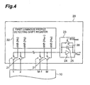
- Fig. 4 is a schematic block diagram showing a first luminous profile detecting signal processing circuit included in the imaging device according to the present embodiment.
- Fig. 5 is a schematic block diagram showing a second luminous profile detecting signal processing circuit included in the imaging device according to the present embodiment.
- Fig. 6A is a graph showing changes over time of a signal outputted from a first luminous profile detecting shift register.
- Fig. 6B is a graph showing changes over time of a signal outputted from the first luminous profile detecting shift register.
- Fig. 6C is a graph showing changes over time of a signal outputted from the first luminous profile detecting shift register.
- Fig. 6D is a graph showing changes over time of a reset signal inputted to a first integrating circuit.
- Fig. 6E is a graph showing changes over time of a voltage outputted from the first luminous profile detecting signal processing circuit.
- Fig. 7A is a graph showing changes over time of a signal outputted from a second luminous profile detecting shift register.
- Fig. 7B is a graph showing changes over time of a signal outputted from the second luminous profile detecting shift register.
- Fig. 7C is a graph showing changes over time of a signal outputted from the second luminous profile detecting shift register.
- Fig. 7D is a graph showing changes over time of a reset signal inputted to a second integrating circuit.
- Fig. 7E is a graph showing changes over time of a voltage outputted from the second luminous profile detecting signal processing circuit.
- Fig. 8 is a schematic block diagram showing an image detecting element included in the imaging device according to the present embodiment.
- Fig. 9A is a graph showing changes over time of a signal outputted from a first image detecting shift register.
- Fig. 9B is a graph showing changes over time of a signal outputted from the first image detecting shift register.
- Fig. 9C is a graph showing changes over time of a signal outputted from a second image detecting shift register.
- Fig. 9D is a graph showing changes over time of a signal outputted from the second image detecting shift register.
- Fig. 9E is a graph showing changes over time of a reset signal inputted to a third integrating circuit.
- Fig. 9F is a graph showing changes over time of a voltage outputted from the third integrating circuit.
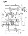
- Fig. 10 is a schematic block diagram showing a modification example of the imaging device according to the present embodiment.
- Fig. 11 is a schematic block diagram showing a modification example of the imaging device according to the present embodiment.
- Fig. 12A is a diagram showing the operation of the modification example of the imaging device shown in Fig. 11.
- Fig. 12B is a diagram showing the operation of the modification example of the imaging device shown in Fig. 11.
- An imaging device according to the present invention will be described with reference to the drawings. In the descriptions that follow, the same constituents or such constituents that have the same functions will be denoted with the same reference numbers, and thus duplicated description is omitted. Hereinafter, parameters M and N are respectively taken as integers of two or greater. In addition, unless otherwise particularly stated, a parameter m is taken as any integer of one or greater but not exceeding M and a parameter n is taken as any integer of one or grater but not exceeding N.
- Fig. 1 is a conceptual schematic diagram showing a configuration of an imaging device according to the present embodiment. As shown in Fig. 1, the
imaging device 1 of this embodiment includes aphotosensitive region 10, a first luminous profile detectingsignal processing circuit 20, a second luminous profile detectingsignal processing circuit 30, and an image detectingsignal processing circuit 50. Here, the first luminous profile detectingsignal processing circuit 20 and the second luminous profile detectingsignal processing circuit 30 constitute a luminous profile detecting element. - In the
photosensitive region 10,pixels 11mn are two-dimensionally arrayed in M rows and N columns. - One of the pixels is configured by disposing a first
photosensitive portion 12mn and a second photosensitive portion 13mn adjacent to each other within the same plane. Thephotosensitive portion 12mn and 13mn respectively output electric currents in accordance with intensities of light that is incident to each of the photosensitive portions. Furthermore, the second photosensitive portion 13mn contains a plurality of (two in this embodiment)photosensitive portions - Across the plurality of
pixels 1111 to 111N, 1121 to 112N,..., and 11M1 to 11MN that are arrayed in a first direction in the two-dimensional array, thephotosensitive portions 14mn on one side (for example, photosensitive portions on oneside 1411 to 141N) among the plurality ofphotosensitive portions photosensitive portions 15mn on the other side (for example, photosensitive portions on theother side 1511 to 151N) among the plurality ofphotosensitive portions - Here, the configuration of the
photosensitive region 10 will be described based on Figs. 2 and 3. Fig. 2 is an enlarged plan view showing an example of a photosensitive region included in the imaging device. Fig. 3 is a schematic block diagram showing a photosensitive region included in the imaging device. - In Fig. 2, depiction of an insulating layer, a protection layer, etc., is omitted.
- The
photosensitive region 10 includes asemiconductor substrate 40 made of P-type (first conductive type) semiconductor, and N-type (second conductive type)semiconductor regions semiconductor substrate 40. - In this way, the first
photosensitive portion 12mn includes thesemiconductor substrate 40 and the second conductivetype semiconductor region 41, thereby constituting aphotodiode 61. Thephotosensitive portions 14mn on one side contained in the second photosensitive portion 13mn includes thesemiconductor substrate 40 and the second conductivetype semiconductor region 42, thereby constituting aphotodiode 62. Thephotosensitive portions 15mn on the other side contained in the second photosensitive portion 13mn includes thesemiconductor substrate 40 and the second conductivetype semiconductor region 43, thereby constituting aphotodiode 63. The firstphotosensitive portion 12mn is constructed as a passive pixel sensor (PPS: Passive Pixel Sensor). - As shown in Fig. 2, each of the second conductive
type semiconductor regions regions semiconductor substrate 40 serves as a ground potential. Thephotosensitive region 10 may also be configured by including a semiconductor substrate made of N-type semiconductor, and P-type semiconductor regions formed on a surface of the semiconductor substrate. - A
first wire 45 is electrically connected to theregions 41 via through-holes (not shown) formed in an insulating layer (not shown). Furthermore,MOS gates 46 made of polysilicon are equipped, and asecond wire 47 is electrically connected to theMOS gates 46. Theregion 41 and theMOS gate 46 constitute a switch element 64 (Field Effect Transistor: FET). The drain of theswitch element 64 corresponds to a large area portion of theregion 41, and the source thereof is connected to thefirst wire 45. - A
third wire 48 is electrically connected to theregions 42 via through-holes (not shown) formed in the insulating layer (not shown). Afourth wire 49 is electrically connected to theregions 43 via through-holes (not shown) formed in the insulating layer (not shown). The insulating layer is made of SiO2, SiN or the like. The first wire 44 to thefourth wire 49 are made of metal such as Al. - The
first wire 45 is for electrically connecting theregions 41 on one side in each of thepixels 11mn in the first direction, and is disposed so as to extend in the first direction among thepixels 11mn. Thesecond wire 47 is for electrically connect theMOS gates 46 in the second direction, and is disposed so as to extend in the second direction among thepixels 11mn. - The
third wire 48 is for electrically connecting theregions 42 in each of thepixels 11mn in the first direction, and is disposed so as to extend in the first direction among thepixels 11mn. Since theregions 42 in each of thepixels 11mn are electrically connected by thethird wire 48 in this way, thephotosensitive portions 14mn on one side (for example, photosensitive portions on oneside 1411 to 141N) are electrically connected to each other, across the plurality ofpixels 1111 to 111N, 1121 to 112N,..., and 11M1 to 11MN that are arrayed in the first direction in the two-dimensional array. Accordingly, a long photosensitive portion extending in the first direction is configured in thephotosensitive region 10. The long photosensitive portions extending in the first direction are formed in M columns. - The
forth wire 49 is for electrically connecting theregions 43 in each of thepixel 11mn in the second direction, and is disposed so as to extend in the second direction among thepixels 11mn. Since theregions 43 in each of thepixels 11mn are electrically connected by theforth wire 49 in this way, thephotosensitive portions 15mn on the other side (for example, photosensitive portions on oneside 1511 to 15M1) are electrically connected to each other, across the plurality ofpixels 1111 to 11M1, 1112 to 11M2,..., and 111N to 11MN that are arrayed in the second direction in the two-dimensional array. Accordingly, a long photosensitive portion extending in the second direction is configured in thephotosensitive region 10. The long photosensitive portions extending in the second direction is formed in N rows. - Furthermore, in the
photosensitive region 10, M columns of the long photosensitive portions extending in the first direction and N rows of the long photosensitive portions extending in the second direction described above are formed on the same plane. - As is apparent from Fig. 2, the
second wire 47 and thefourth wire 49 are connected to each other among thepixels 11 arrayed in the right-and-left direction in Fig. 3, and thefirst wire 45 and thethird wire 48 are connected to each other among thepixels 11 arrayed in the up-and-down direction in Fig. 3. - Shapes of the
regions - Hereinafter, configurations of the first luminous profile detecting
signal processing circuit 20 and the second luminous profile detectingsignal processing circuit 30 will be described based on Figs. 4 and 5. Fig. 4 is a schematic block diagram showing the first luminous profile detecting signal processing circuit, and Fig. 5 is a schematic block diagram showing the second luminous profile detecting signal processing circuit. - The first luminous profile detecting
signal processing circuit 20 outputs a voltage Hout that indicates a luminous profile in the second direction of incident light to thephotosensitive region 10. The second luminous profile detectingsignal processing circuit 30 outputs a voltage Vout that indicates a luminous profile in the first direction of incident light to thephotosensitive region 10. - The first luminous profile detecting
signal processing circuit 20 outputs a voltage Hout indicating the luminous profile in the second direction of light incident to thephotosensitive region 10. The second luminous profile detectingsignal processing circuit 30 outputs a voltage Vout indicating the luminous profile in the first direction of light incident to thephotosensitive region 10. - As shown in Fig. 4, the first luminous profile detecting
signal processing circuit 20 includes first switches 21, a first luminous profile detectingshift register 22, and a first integratingcircuit 23. The first switches 21 are provided corresponding to each relevant group ofphotosensitive portions 14mn on one side (M columns of long photosensitive portions configured of the second conductivetype semiconductor regions 42, extending in the first direction). Thesephotosensitive portions 14mn are electrically connected across the plurality ofpixels 1111 to 111N, 1121 to 112N,..., and 11M1 to 11MN arrayed in the first direction. The first luminous profile detectingshift register 22 sequentially reads electric currents in the second direction. The electric currents are from the group ofphotosensitive portions 14mn on one side that are electrically connected across the plurality ofpixels 1111 to 111N, 1121 to 112N,..., and 11M1 to 11MN arrayed in the first direction. The first integratingcircuit 23 sequentially receives the electric currents, which are from each group ofphotosensitive portions 14mn on one side and are sequentially connected by the first luminous profile detectingshift register 22. Then, the first integratingcircuit 23 converts the electric current into voltage and outputs the voltage. - The first switches 21 are controlled by a signals shift (Hm) outputted from the first luminous profile detecting
shift register 22, and then are sequentially closed. Electric charges are accumulated in the group ofphotosensitive portions 14mn on one side that are electrically connected across the plurality ofpixels 1111 to 111N, 1121 to 112N,..., and 11M1 to 11MN arrayed in the first direction. By closing thefirst switches 21, the above accumulated electric charges are changed into electric currents, which are then outputted to the first integratingcircuit 23 through thethird wires 48 and the first switches 21. Operations of the first luminous profile detectingshift register 22 are controlled by signals outputted from a control circuit (not shown), thus closing thefirst switches 21 sequentially. - The first integrating
circuit 23 includes anamplifier 24, acapacitor 25, and aswitch 26. Theamplifier 24 is inputted the electric currents from the groups ofphotosensitive portions 14mn on one side that are electrically connected across the plurality ofpixels 1111 to 111N, 1121 to 112N,..., and 11M1 to 11MN arrayed in the first direction, and amplifies electric charges of the inputted electric currents. In thecapacitor 25, one terminal thereof is connected to an input terminal of theamplifier 24, and the other terminal thereof is connected to an output terminal of theamplifier 24. In theswitch 26, one terminal thereof is connected to the input terminal of theamplifier 24, and the other terminal thereof is connected to the output terminal of theamplifier 24. Theswitch 26 is turned to an "ON" state when a reset signal ΦHreset outputted from the control circuit is significant, and is turned to an "OFF" state when the reset signal ΦHreset is insignificant. - When the
switch 26 is in the "ON" state, the first integratingcircuit 23 discharges electricity to reset thecapacitor 25. On the other hand, when theswitch 26 is in the "OFF" state, the first integratingcircuit 23 accumulates the electric charges in thecapacitor 25. These electric charges have been inputted to the input terminal from the groups ofphotosensitive portions 14mn on one side that are electrically connected across the plurality ofpixels 1111 to 111N, 1121 to 112N,..., and 11M1 to 11MN arrayed in the first direction. Thereafter, the first integratingcircuit 23 outputs voltages Hout corresponding to the above-mentioned accumulated electric charges. - As shown in Fig. 5, the second luminous profile detecting
signal processing circuit 30 includes second switches 31, a second luminous profile detectingshift register 32, and a second integratingcircuit 33. The second switches 31 are provided corresponding to each relevant group ofphotosensitive portions 15mn on the other side (N rows of long photosensitive portions configured of the second conductivetype semiconductor regions 43, extending in the second direction). Thesephotosensitive portions 15mn are electrically connected across the plurality ofpixels 1111 to 11M1, 1112 to 11M2,..., and 111N to 11MN arrayed in the second direction. The second luminous profile detectingshift register 32 sequentially reads electric currents in the first direction. The electric currents are from the groups ofphotosensitive portions 15mn on the other side that are electrically connected across the plurality ofpixels 1111 to 11M1, 1112 to 11M2,..., and 111N to 11MN arrayed in the second direction. The second integratingcircuit 33 is sequentially inputted of the electric currents, which are from each group ofphotosensitive portions 15mn on the other side and are sequentially connected by the second luminous profile detectingshift register 32. Then, the second integratingcircuit 33 converts the electric currents into voltages and outputs the voltages. - The second switches 31 are controlled by a signals shift (Vn) outputted from the second luminous profile detecting
shift register 32, and then are sequentially closed. Electric charges are accumulated in the groups ofphotosensitive portions 15mn on the other side that are electrically connected across the plurality ofpixels 1111 to 11M1, 1112 to 11M2,..., and 111N to 11MN arrayed in the second direction. By closing the second switches 31, the above accumulated electric charges are changed into electric currents, which are then inputted to the second integratingcircuit 33 through theforth wires 49 and the second switches 31. Operations of the second luminous profile detectingshift register 32 are controlled by signals outputted from a control circuit (not shown), thus closing thesecond switches 31 sequentially. - The second integrating
circuit 33 includes anamplifier 34, acapacitor 35, and aswitch 36. Theamplifier 34 is inputted the electric currents from the groups ofphotosensitive portions 15mn on the other side that are electrically connected across the plurality ofpixels 1111 to 11M1, 1112 to 11M2,..., and 111N to 11MN arrayed in the second direction, and amplifies electric charges of the inputted electric currents. In thecapacitor 35, one terminal thereof is connected to an input terminal of theamplifier 34, and the other terminal thereof is connected to an output terminal of theamplifier 34. In theswitch 36, one terminal thereof is connected to the input terminal of theamplifier 34, and the other terminal thereof is connected to the output terminal of theamplifier 34. Theswitch 36 is turned to an "ON" state when a reset signal ΦVreset outputted from the control circuit is significant, and is turned to an "OFF" state when the reset signal ΦVreset is insignificant. - When the
switch 36 is in the "ON" state, the second integratingcircuit 33 discharges electricity to reset thecapacitor 35. On the other hand, when theswitch 36 is in the "OFF" state, the second integratingcircuit 33 accumulates the electric charges in thecapacitor 35. These electric charges have been inputted to the input terminal from the groups ofphotosensitive portions 15mn on the other side that are electrically connected across the plurality ofpixels 1111 to 11M1, 1112 to 11M2,..., and 111N to 11MN arrayed in the second direction. Thereafter, the second integratingcircuit 33 outputs voltages Vout corresponding to the above-mentioned accumulated electric charges. - Hereinafter, operations of the first luminous profile detecting
signal processing circuit 20 and the second luminous profile detectingsignal processing circuit 30 will be described based on Figs. 6A to 6E and Figs. 7A to 7E. Figs. 6A to 6E are timing charts for explaining the operations of the first luminous profile detecting signal processing circuit. Figs. 7A to 7E are timing charts for explaining the operations of the second luminous profile detecting signal processing circuit. - As shown in Fig. 6A and Fig. 6B, after the start signal is inputted to the first luminous profile detecting
shift register 22 from the control circuit, signals shift (Hm), each having a predetermined pulse width, are sequentially outputted. When the first luminous profile detectingshift register 22 outputs the shift (Hm) to each of the correspondingfirst switches 21, thefirst switches 21 are sequentially closed. Thereafter, the electric charges accumulated in the corresponding group ofphotosensitive portions 14mn on one side are turned into electric currents and are sequentially inputted to the first integratingcircuits 23. - As shown in Fig. 6D, the reset signal ΦHreset is inputted to the first integrating
circuit 23 from the control circuit. While the reset signal ΦHreset is in an "OFF" state, the electric charges accumulated in the corresponding group ofphotosensitive portions 14mn on one side are accumulated in thecapacitor 25. Then, as shown in Fig. 6E, voltages Hout corresponding to amounts of the accumulated electric charges are sequentially outputted from the first integratingcircuit 23. When the reset signal ΦHreset is in an "ON" state, the first integratingcircuit 23 closes theswitch 26 and reset thecapacitor 25. - In this way, the first luminous profile detecting
signal processing circuit 20 sequentially outputs the voltages Hout as time-series data of each of the corresponding groups ofphotosensitive portions 14mn on one side. The voltages Hout correspond to the electric charges (electric currents) accumulated in the groups ofphotosensitive portions 14mn on one side that are electrically connected across the plurality ofpixels 1111 to 111N, 1121 to 112N,..., and 11M1 to 11MN arrayed in the first direction. The time-series data indicates a luminous profile in the second direction. - As shown in Fig. 7A and Fig. 7B, After the start signal is inputted to the second luminous profile detecting
shift register 32 from the control circuit, signals shifts (Vn), each having a predetermined pulse width, are sequentially outputted. When the second luminous profile detectingshift register 32 outputs the shift (Vn) to each of the correspondingsecond switches 31, thesecond switches 31 are sequentially closed. Thereafter, the electric charges accumulated in the corresponding group ofphotosensitive portions 15mn on one side are turned into electric currents and are sequentially inputted to the second integratingcircuits 33. - As shown in Fig. 7D, the reset signal ΦVreset is inputted to the second integrating
circuit 33 from the control circuit. While the reset signal ΦVreset is in an "OFF" state, the electric charges accumulated in the corresponding group ofphotosensitive portions 15mn on the other side are accumulated in thecapacitor 35. Then, as shown in Fig. 7E, voltages Vout corresponding to amounts of the accumulated electric charges are sequentially outputted from the second integratingcircuit 33. When the reset signal ΦVreset is in an "ON" state, the second integratingcircuit 33 closes theswitch 36 and reset thecapacitor 35. - In this way, the second luminous profile detecting
signal processing circuit 30 sequentially outputs the voltages Vout as time-series data of each of the corresponding groups ofphotosensitive portions 15mn on the other side. The voltages Vout correspond to the electric charges (electric currents) accumulated in the groups ofphotosensitive portions 15mn on the other side that are electrically connected across the plurality ofpixels 1111 to 11M1, 1112 to 11M2,..., and 111N to 11MN arrayed in the first direction. The time-series data indicates a luminous profile in the second direction. - Hereinafter, configurations of the image detecting
signal processing circuit 50 will be described based on Figs. 8. Fig. 8 is a schematic block diagram showing a image detecting element. The image detectingsignal processing circuit 50 outputs a voltage IMout indicating pixel data (image) corresponding to incident light to thephotosensitive region 10. - The image detecting
signal processing circuit 50 includes a first image detectingshift register 51,third switches 52, a second image detectingshift register 53, and a third integratingcircuit 54. The first image detectingshift register 51 sequentially reads electric currents from each firstphotosensitive portion 12mn in the first direction. The third switches 52 are provided corresponding to thepixels 11mn arrayed in the second direction. The second image detectingshift register 53 sequentially reads the electric currents, which are sequentially read in the first direction by the first image detectingshift register 51, in the second direction. The third integratingcircuit 54 sequentially receive the electric currents, which are from each firstphotosensitive portion 12mn and are sequentially connected by the second image detectingshift register 53. Then, The third integratingcircuits 54 converts the electric current into voltage and outputs the voltage. - Operations of the first image detecting
shift register 51 are controlled by signals outputted from the control circuit (not shown) to read the electric current from each firstphotosensitive portion 12mn, and outputs a signal shift (VIn) to each MOS gate 46 (switch element 64). The first image detectingshift register 51 is connected through thesecond wire 47 to the MOS gates 46 (switch elements 64) of the firstphotosensitive portions 12mn arrayed in the second direction so that the signal shift (VIN) can be simultaneously output to theMOS gates 46. - The third switches 52 are controlled by a signals shift (HIm) outputted from the second image detecting
shift register 53, and then are sequentially closed. Electric charges are accumulated in the firstphotosensitive portion 12mn corresponding to the MOS gate 46 (switch element 64) closed by the signal shift (VIn) from the first image detectingshift register 51.
By closing thethird switches 52, the above accumulated electric charges are changed into electric currents, which are then outputted to the third integratingcircuit 54 through thefirst wires 45 and the third switches 52. Operations of the second image detectingshift register 53 are controlled by signals outputted from a control circuit (not shown), thus closing thethird switches 52 sequentially. - The third integrating
circuit 54 includes anamplifier 55, acapacitor 56, and aswitch 57. Theamplifier 55 is inputted the electric currents from each firstphotosensitive portion 12mn, and amplifies electric charges of the inputted electric currents. In thecapacitor 56, one terminal thereof is connected to an input terminal of theamplifier 55, and the other terminal thereof is connected to an output terminal of theamplifier 55. In theswitch 57, one terminal thereof is connected to the input terminal of theamplifier 55, and the other terminal thereof is connected to the output terminal of theamplifier 55. Theswitch 57 is turned to an "ON" state when a reset signal ΦIMreset outputted from the control circuit is significant, and is turned to an "OFF" state when the reset signal ΦIMreset is insignificant. - When the
switch 57 is in the "ON" state, the third integratingcircuit 54 discharges electricity to reset thecapacitor 56. On the other hand, when theswitch 57 is in the "OFF" state, the third integratingcircuit 54 accumulates the electric charges in thecapacitor 56. These electric charges have been inputted to the input terminal from each firstphotosensitive portion 12mn. Thereafter, the third integratingcircuit 54 outputs voltages IMout corresponding to the above-mentioned accumulated electric charges. - Hereinafter, operations of the image detecting
signal processing circuit 50 will be described based on Figs. 9A to 9F. Figs. 9A to 9F are timing charts for explaining the operations of the image detecting signal processing circuit. - As shown in Fig. 9A and Fig. 9B, after the start signal is inputted to the first image detecting
shift register 51 from the control circuit, signals shifts (VIn), each having a predetermined pulse width, are sequentially outputted. When the first image detectingshift register 51 outputs the shift (VIn) to each of the correspondingMOS gates 46, theMOS gates 46 are sequentially closed. - As shown in Fig. 9C and Fig. 9D, when the start signal is inputted from the control circuit to the second image detecting
shift register 53 under the above state, signals shift (HIm) each having a predetermined pulse width, are sequentially outputted. When the second image detectingshift register 53 outputs the shift (HIn) to each of the correspondingthird switches 52, thethird switches 52 are sequentially closed. Thereafter, the electric charges accumulated in the corresponding firstphotosensitive portions 12mn are turned into electric currents and are sequentially inputted to the third integratingcircuit 54. - As shown in Fig. 9E, the reset signal ΦIMreset is inputted to the third integrating
circuit 54 from the control circuit. While the reset signal ΦIMreset is in an "OFF" state, the electric charges accumulated in the corresponding firstphotosensitive portion 12mn are accumulated in thecapacitor 56. Then, as shown in Fig. 9F, voltages IMout corresponding to amounts of the accumulated electric charges are sequentially outputted from the third integratingcircuit 54. When the reset signal ΦIMreset is in an "ON" state, the third integratingcircuit 54 closes theswitch 57 and reset thecapacitor 56. - In this way, the image detecting
signal processing circuit 50 sequentially outputs the voltages IMout, corresponding to the electric charges (electric currents) accumulated in the firstphotosensitive portion 12mn, as time-series data of each of the corresponding firstphotosensitive portion 12mn. The time-series data indicates pixel data (image). - The first luminous profile detecting
signal processing circuit 20, the second luminous profile detectingsignal processing circuit 30 and the image detectingsignal processing circuit 50 may be operated simultaneously or individually in a time-series order. - As described above, in the
imaging device 1 of this embodiment, light incident on onepixel 11mn is detected by each of the firstphotosensitive portion 12mn and the second photosensitive portion 13mn that configure thepixel 11mn concerned, and the output corresponding to the light intensity is gained for everyphotosensitive portion 12mn and 13mn. The image detectingsignal processing circuit 50 reads out the output from the firstphotosensitive portion 12mn and detects an image on the basis of the output concerned. Furthermore, the luminous profile detecting element (the first luminous profile detectingsignal processing circuit 20 and the second luminous profile detecting signal processing circuit 30) reads out the output from the second photosensitive portion 13mn, and detects the luminous profiles in the first direction and the second direction in the two-dimensional array on the basis of the output concerned. Since one pixel is configured by the firstphotosensitive portion 12mn and the second photosensitive portion 13mn, it is possible to detect both the image and two-dimensional positions to where light is incident. - Furthermore, in the
imaging device 1 of this embodiment, thefirst wire 45 and thesecond wire 47 for leading the outputs from the firstphotosensitive portions 12mn to the image detectingsignal processing circuit 50, and thethird wire 48 and thefourth wire 49 for leading the outputs from the second photosensitive portions 13mn to the luminous profile detecting element (the first luminous profile detectingsignal processing circuit 20 and the second luminous profile detecting signal processing circuit 30) are disposed so as to extend between thepixels 11mn. Accordingly, each of thewires photosensitive portions 12mn and the second photosensitive portions 13mn, thus suppressing a detection sensitivity reduction. - Still furthermore, in the
imaging device 1 of this embodiment, the second photosensitive portion 13mn contains a plurality ofphotosensitive portions photosensitive portions 14mn on one side, amongst the plurality ofphotosensitive portions pixels 1111 to 111N, 1121 to 112N, ..., 11M1 to 11MN arrayed in the first direction in the two-dimensional array; and thephotosensitive portions 15mn on the other side, amongst the plurality ofphotosensitive portions pixels 1111 to 11M1, 1112 to 11M2, ..., 111N to 11MN arrayed in the first direction in the two-dimensional array. Accordingly, light incident to second photosensitive portion 13mn is detected by each of thephotosensitive portions photosensitive portion photosensitive portions 14mn on one side are electrically connected to each other across the plurality ofpixels 1111 to 111N, 1121 to 112N, ..., 11M1 to 11MN arrayed in the first direction in the two-dimensional array, electric currents from thephotosensitive portions 14mn on one side are thereafter transmitted to the first direction. Furthermore, since thephotosensitive portions 15mn on the other side are electrically connected to each other across the plurality ofpixels 1111 to 11M1, 1112 to 11M2, ..., 111N to 11MN arrayed in the second direction in the two-dimensional array, electric currents from thephotosensitive portions 15mn on the other side are thereafter transmitted to the second direction. As described above, the electric currents from thephotosensitive portions 14mn on one side are transmitted in the first direction, and the electric currents from thephotosensitive portions 15mn on the other side are transmitted in the second direction, so that both of the luminous profile in the first direction and the luminous profile in the second direction are obtained independently. As a result, fast detection of the two-dimensional positions of the incident light becomes possible with an extremely simple structure that a plurality ofphotosensitive portions - Furthermore, in the
imaging device 1 of this embodiment, it is preferable that thethird wire 48 is disposed so as to extend in the first direction between thepixels 11mn, and thefourth wire 49 is disposed so as to extend in the second direction between thepixels 11mn. In the case of the above construction, each of thewires photosensitive portions 12mn and 13mn, thus suppressing a detection sensitivity reduction. - Still furthermore, in the
imaging device 1 of this embodiment, the second photosensitive portion 13mn outputs the electric current corresponding to the intensity of incident light, and the luminous profile detecting element (the first luminous profile detectingsignal processing circuit 20, the second luminous profile detecting signal processing circuit 30) contain the first luminous profile detectingshift register 22, the second luminous profile detectingshift register 32, the first integratingcircuit 23, and the second integratingcircuit 33. Accordingly, the luminous profile in the first direction and the luminous profile in the second direction can be obtained with an extremely simple structure. - Still furthermore, in the
imaging device 1 of this embodiment, the firstphotosensitive portion 12mn outputs the electric current corresponding to the intensity of incident light, and the image detectingsignal processing circuit 50 contains the first image detectingshift register 51, the second image detectingshift register 53, and the second integratingcircuit 54. Accordingly, the image (pixel data) can be obtained with an extremely simple structure. - Next, a modification example of the imaging device according to the above embodiment will be described based on Fig. 10. Fig. 10 is a schematic block diagram showing a modification example of the imaging device according to the above embodiment. The modification example differs from the above embodiment in that the first
photosensitive portion 12mn is constructed as an active pixel sensor (PPS: Active Pixel Sensor). In Fig. 10, it is illustrated as 2x2 pixels. In Fig. 10, respective wires extending from the same positions ofrespective pixels - Respective drains of field effect transistors (FET) 81 and 82 are connected to a power supply voltage, and a source of the
transistor 81 and a gate of thetransistor 82 are connected to a drain of afield effect transistor 83. A source of thetransistor 83 is connected to a cathode of thephotodiode 61. Furthermore, a source of thetransistor 82 is connected through a drain and a source of atransistor 84 to athird switch element 52. A reset signal Reset (VIn) is supplied from the first image detectingshift register 51 to a gate of thetransistor 81, and a signal SW (VIn) from the first image detectingshift register 51 to a gate of thetransistor 83. Furthermore, a signal shift (VIn) is supplied from the first image detectingshift register 51 to thetransistor 84. - Operations of the active pixel sensor will be described. First, the reset signal Reset (VIn) is applied to the gate of the
transistor 81 to turn on thetransistor 81, and the cathodic potential of thephotodiode 61 is set to the power supply potential (reset) via the drain and the source of thetransistor 81. At this time, thetransistor 83 is turned on, and thetransistor 84 is turned off. Subsequently, the reset signal Reset (VIn) to the gate of thetransistor 81 is quenched, and thus thetransistor 81 is turned off, whereby the cathodic potential of thephotodiode 61 is kept to the power supply potential. Under this state, light is irradiated to thephotodiode 61, thephotodiode 61 photoelectrically converts the incident light, and the charges Q proportional to the irradiation light amount (intensity x time) are accumulated in thephotodiode 61, so that the cathodic potential of thephotodiode 61 suffers voltage variation of Q/C (here, C represents the capacitance of the photodiode 61). - Thereafter, the signal SW (VIn) is applied to the gate of the
transistor 83, and the signal shift (VIn) is applied to the gate of thetransistor 84, whereby the cathode voltage variation of thephotodiode 61 described above is output as an image signal through thetransistor 83, thetransistor 82 and thetransistor 84. - In this way, even when the first
photosensitive portion 12mn is constructed by the active pixel sensor, it is possible to detect both the image and two-dimensional positions to where light is incident. - Next, another modification example of the imaging device according to the above embodiment will be described based on Fig. 11. Fig. 11 is a schematic block diagram showing a modification example of the imaging device according to the above embodiment.
- In the modification shown in Fig. 11, the second luminous profile detecting signal processing circuit 30 (the luminous profile detecting element) includes a first pixel
position specifying portion 91 for specifying pixel positions of a predetermined luminous or more in the luminous profile in the first direction.
The output from eachsecond switch 31 is connected to the first pixelposition specifying portion 91 so that the electric currents from the group ofphotosensitive portions 15mn on the other side are inputted to the first pixelposition specifying portion 91. Thephotosensitive portions 15mn on the other side are electrically connected to each other, across the plurality ofpixels 1111 to 11M1, 1112 to 11M2,..., and 111N to 11MN that are arrayed in the second direction. - The first pixel
position specifying portion 91 specifies the pixel positions of the predetermined luminous or more on the basis of the inputted outputs, and outputs the information on the specified pixel positions as pixel information (channel information) to the first image detectingshift register 51. The pixel information contains pixel positions located around the pixel positions thus specified. The first image detectingshift register 51 sequentially outputs the shift (VIn) to only theMOS gates 46 corresponding to the pixel positions in the pixel information concerned on the basis of the pixel information fed from the first pixelposition specifying portion 91, whereby only theMOS gates 46 corresponding to the pixel positions in the pixel information are sequentially closed. - The first luminous profile detecting signal processing circuit 20 (the luminous profile detecting element) includes a second pixel
position specifying portion 92 for specifying pixel positions of a predetermined luminous or more in the luminous profile in the second direction. The output from eachfirst switch 21 is connected to the second pixelposition specifying portion 92 so that the electric currents from the group ofphotosensitive portions 14mn on one side are inputted to the second pixelposition specifying portion 92. Thephotosensitive portions 14mn on one side are electrically connected to each other, across the plurality ofpixels 1111 to 111N, 1121 to 112N,..., and 11M1 to 11MN that are arrayed in the first direction. - The second pixel
position specifying portion 92 specifies the pixel positions of the predetermined luminous or more on the basis of the inputted outputs, and outputs the information on the specified pixel positions as pixel information (channel information) to the second image detectingshift register 53. The pixel information contains pixel positions located around the specified pixel positions. The second image detectingshift register 53 sequentially outputs the shift (HIm) to only thethird switch elements 52 corresponding to the pixel positions in the pixel information. Accordingly, only thethird switch elements 52 corresponding to the pixel positions in the pixel information are sequentially closed, and the charges accumulated in the firstphotosensitive portions 12mn corresponding to the pixel positions concerned are sequentially output as electric current through an image read-out circuit 93 and thethird switch elements 52 to an A/D converting circuit 94. The outputs of the first luminous profile detectingsignal processing circuit 20 and the second luminous profile detectingsignal processing circuit 30 are fed to A/D converting circuits - Accordingly, as shown in Fig. 12A and Fig. 12B, an image I2 (O x P pixels: M≥O, N≥P) of a predetermined area in which the luminous is equal to the predetermined luminous or more can be achieved for an image I1 (M x N pixels) detected in the overall
photosensitive region 10. For example, under a condition where M=N=512, O=P=64 and the reading speed is set to 1µsec/pixel, when the image I1 is read out, the frame rate is equal to 3.8 (fps), and when theimage 12 is read out, the frame rate is equal to 244 (fps). In this way, it is possible to read image at high speed. In Fig. 12A, a characteristic A indicates the luminous profile in the second direction which is obtained by the first luminous profile detectingsignal processing circuit 20, and a characteristic B indicates the luminous profile in the first direction which is obtained by the second luminous profile detectingsignal processing circuit 30. - As described above, in the modification shown in Fig. 11, the image containing the area having the predetermined luminous or more can be detected at an extremely high speed. Furthermore, the
imaging device 1 is applicable to a moving body tracking sensor or the like. - The present invention is not limited to the above embodiments. For example, in place of the arrangement where the second photosensitive portions 13mn are disposed so as to be adjacent to the first
photosensitive portions 12mn on the same plane, a grid-shaped resistive element such as a ohmic electrode or the like may be disposed on the back side of thesemiconductor substrate 40 on which thephotosensitive region 10 is formed, and a change in resistance based on light incidence may be detected to obtain the luminous profile (light incident position) in the first direction and second direction. - The imaging device of the present invention can be applied for a moving body tracking device.
Claims (7)
- An imaging device having a photosensitive region containing two-dimensionally arranged pixels,
wherein one pixel is configured by a first photosensitive portion and a second photosensitive portion which output corresponding to the intensity of light incident thereto, and
the imaging device comprises an image detecting element for reading an output from the first photosensitive portion and detecting an image on the basis of the output concerned; and
a luminous profile detecting element for reading out an output from the second photosensitive portion and detecting luminous profiles in a first direction and a second direction in the two-dimensional array on the basis of the output concerned. - The imaging device according to Claim 1,
wherein a wire for leading the outputs from the first photosensitive portions to the image detecting element and a wire for leading the outputs from the second photosensitive portions to the luminous profile detecting element are disposed so as to extend between the pixels. - The imaging device according to Claim 1,
wherein the second photosensitive portion contains a plurality of photosensitive portions which are arranged so as to be adjacent to one another on the same plane,
the photosensitive portions on one side, amongst the plurality of photosensitive portions contained in the second photosensitive portions, are electrically connected to each other across the plurality of pixels arrayed in the first direction in the two-dimensional array; and
the photosensitive portions on the other side, amongst the plurality of photosensitive portions contained in the second photosensitive portions, are electrically connected to each other across the plurality of pixels arrayed in the first direction in the two-dimensional array. - The imaging device according to Claim 3,
wherein a wire is provided for electrically connecting the photosensitive portions on one side, amongst the plurality of photosensitive portions contained in the second photosensitive portions, to each other across the plurality of pixels arrayed in the first direction, the wire is disposed so as to extend in the first direction between the pixels, and
a wire is provided for electrically connecting the photosensitive portions on one side, amongst the plurality of photosensitive portions contained in the second photosensitive portions, to each other across the plurality of pixels arrayed in the second direction, the wire is disposed so as to extend in the second direction between the pixels. - The imaging device according to Claim 3,
wherein the second photosensitive portion outputs an electric current corresponding to the intensity of incident light, and
the luminous profile detecting element comprises: a first luminous profile detecting shift register for sequentially reading electric currents in the second direction, the electric currents being from groups of the photosensitive portions on one side which are electrically connected across the plurality of pixels arrayed in the first direction;
a second luminous profile detecting shift register for sequentially reading electric currents in the first direction, the electric currents being from groups of the photosensitive portions on one side which are electrically connected across the plurality of pixels arrayed in the second direction;
a first integrating circuit for sequentially receiving the electric currents from each of the groups of photosensitive portions on one side, the electric currents being sequentially read by the first luminous profile detecting shift register, and converts the electric currents into voltages; and
a second integrating circuit for sequentially receiving the electric currents from each of the groups of photosensitive portions on the other side, the electric currents being sequentially read by the second luminous profile detecting shift register, and converts the electric currents into voltages. - The imaging device according to Claim 1,
wherein the first photosensitive portion outputs an electric current corresponding to the intensity of incident light, and
the image detector comprises a first image detecting shift register for sequentially reading electric currents from the first photosensitive portions in the second direction; and
a second image detecting shift register for sequentially reading electric currents in the second direction, the electric currents being sequentially read by first image detecting shift register. - The imaging device according to Claim 1,
wherein the luminous profile detecting element contains a first image position specifying element for specifying pixel positions having predetermined luminous or more in the detected luminous profile in the first direction; and
a second image position specifying element for specifying pixel positions having predetermined luminous or more in the detected luminous profile in the second direction, and
wherein the image detecting element detects an image containing the respective pixel positions specified by the first pixel position specifying element and the second pixel position specifying element.
Applications Claiming Priority (3)
| Application Number | Priority Date | Filing Date | Title |
|---|---|---|---|
| JP2001389567 | 2001-12-21 | ||
| JP2001389567A JP3965049B2 (en) | 2001-12-21 | 2001-12-21 | Imaging device |
| PCT/JP2002/012887 WO2003055201A1 (en) | 2001-12-21 | 2002-12-10 | Imaging device |
Publications (2)
| Publication Number | Publication Date |
|---|---|
| EP1460839A1 true EP1460839A1 (en) | 2004-09-22 |
| EP1460839A4 EP1460839A4 (en) | 2006-03-15 |
Family
ID=19188273
Family Applications (1)
| Application Number | Title | Priority Date | Filing Date |
|---|---|---|---|
| EP02786068A Withdrawn EP1460839A4 (en) | 2001-12-21 | 2002-12-10 | IMAGING DEVICE |
Country Status (8)
| Country | Link |
|---|---|
| US (1) | US7245317B2 (en) |
| EP (1) | EP1460839A4 (en) |
| JP (1) | JP3965049B2 (en) |
| KR (1) | KR100876729B1 (en) |
| CN (1) | CN100512392C (en) |
| AU (1) | AU2002354122A1 (en) |
| TW (1) | TWI248215B (en) |
| WO (1) | WO2003055201A1 (en) |
Cited By (5)
| Publication number | Priority date | Publication date | Assignee | Title |
|---|---|---|---|---|
| EP1713258A3 (en) * | 2005-04-11 | 2008-02-20 | Canon Kabushiki Kaisha | Focus detection |
| EP1845713A4 (en) * | 2005-02-03 | 2009-07-08 | Hamamatsu Photonics Kk | SEMICONDUCTOR IMAGE RECOVERING DEVICE |
| EP1775944A4 (en) * | 2004-06-24 | 2009-09-16 | Hamamatsu Photonics Kk | Distortion detection system and distortion detection method |
| US7800038B2 (en) * | 2004-02-02 | 2010-09-21 | Hamamatsu Photonis K.K. | Photodetector device |
| EP1883036A4 (en) * | 2005-04-28 | 2011-12-28 | Hamamatsu Photonics Kk | DEVICE FOR READING SEMICONDUCTOR IMAGES |
Families Citing this family (13)
| Publication number | Priority date | Publication date | Assignee | Title |
|---|---|---|---|---|
| US7329851B2 (en) | 2003-01-22 | 2008-02-12 | Hamamatsu Photonics K.K. | Photodetector having a photosensitive region and two-dimensional pixel arrangement |
| JP2004264332A (en) * | 2003-01-24 | 2004-09-24 | Hamamatsu Photonics Kk | Multiple image forming position shift detecting device, image density detecting device, and multiple image forming device |
| JP2004264034A (en) * | 2003-01-24 | 2004-09-24 | Hamamatsu Photonics Kk | Photodetector |
| JP4099413B2 (en) | 2003-03-20 | 2008-06-11 | 浜松ホトニクス株式会社 | Photodetector |
| JP2004289709A (en) * | 2003-03-25 | 2004-10-14 | Toshiba Corp | Imaging device and imaging method |
| JP4391315B2 (en) | 2004-05-10 | 2009-12-24 | 浜松ホトニクス株式会社 | Imaging system and imaging method |
| JP4503481B2 (en) * | 2005-04-05 | 2010-07-14 | 浜松ホトニクス株式会社 | Solid-state imaging device |
| US7282685B2 (en) * | 2005-04-14 | 2007-10-16 | Micron Technology, Inc. | Multi-point correlated sampling for image sensors |
| JP4696877B2 (en) * | 2005-11-29 | 2011-06-08 | ヤマハ株式会社 | Solid-state imaging device |
| AT504582B1 (en) * | 2006-11-23 | 2008-12-15 | Arc Austrian Res Centers Gmbh | METHOD FOR GENERATING AN IMAGE IN ELECTRONIC FORM, PICTURE ELEMENT FOR AN IMAGE SENSOR FOR GENERATING AN IMAGE AND PICTOR SENSOR |
| JP4922776B2 (en) * | 2007-01-30 | 2012-04-25 | 富士フイルム株式会社 | Imaging apparatus and imaging method |
| CN104243843B (en) * | 2014-09-30 | 2017-11-03 | 北京智谷睿拓技术服务有限公司 | Pickup light shines compensation method, compensation device and user equipment |
| JP7060413B2 (en) | 2018-03-08 | 2022-04-26 | 浜松ホトニクス株式会社 | Photodetector and photodetection method |
Family Cites Families (31)
| Publication number | Priority date | Publication date | Assignee | Title |
|---|---|---|---|---|
| JPH04151129A (en) | 1990-04-20 | 1992-05-25 | Olympus Optical Co Ltd | Light measuring instrument of camera with tracking device |
| JP2974809B2 (en) | 1991-03-05 | 1999-11-10 | オリンパス光学工業株式会社 | Solid-state imaging device |
| JPH065832A (en) * | 1992-06-19 | 1994-01-14 | Fujitsu Ltd | Apparatus and method for position detection |
| JP3441761B2 (en) * | 1993-05-28 | 2003-09-02 | キヤノン株式会社 | Image sensor |
| US5406070A (en) * | 1993-12-16 | 1995-04-11 | International Business Machines Corporation | Method and apparatus for scanning an object and correcting image data using concurrently generated illumination data |
| JP2731115B2 (en) * | 1994-07-14 | 1998-03-25 | シャープ株式会社 | Split type light receiving element |
| KR960028217A (en) * | 1994-12-22 | 1996-07-22 | 엘리 웨이스 | Motion Detection Camera System and Method |
| JPH08292998A (en) * | 1995-04-20 | 1996-11-05 | Mitsubishi Electric Corp | Image detecting device and image detecting method |
| WO1997007630A1 (en) * | 1995-08-11 | 1997-02-27 | Kabushiki Kaisha Toshiba | Mos image pickup device |
| KR100279295B1 (en) * | 1998-06-02 | 2001-02-01 | 윤종용 | Active pixel sensor |
| US6956605B1 (en) * | 1998-08-05 | 2005-10-18 | Canon Kabushiki Kaisha | Image pickup apparatus |
| JP4812940B2 (en) * | 1998-10-30 | 2011-11-09 | 浜松ホトニクス株式会社 | Solid-state imaging device array |
| WO2000045592A1 (en) | 1999-01-29 | 2000-08-03 | Hamamatsu Photonics K.K. | Photodetector device |
| JP3449468B2 (en) | 1999-05-06 | 2003-09-22 | 日本電気株式会社 | Solid-state imaging device and driving method thereof |
| US6867806B1 (en) * | 1999-11-04 | 2005-03-15 | Taiwan Advanced Sensors Corporation | Interlace overlap pixel design for high sensitivity CMOS image sensors |
| JP4424796B2 (en) * | 1999-11-18 | 2010-03-03 | 浜松ホトニクス株式会社 | Photodetector |
| EP1102323B1 (en) * | 1999-11-19 | 2012-08-15 | CSEM Centre Suisse d'Electronique et de Microtechnique SA - Recherche et Développement | Method for detecting electromagnetic radiation using an optoelectronic sensor |
| JP2001177144A (en) * | 1999-12-20 | 2001-06-29 | Hamamatsu Photonics Kk | Optical position detector |
| JP4500434B2 (en) * | 2000-11-28 | 2010-07-14 | キヤノン株式会社 | Imaging apparatus, imaging system, and imaging method |
| JP2003204488A (en) * | 2001-10-30 | 2003-07-18 | Mitsubishi Electric Corp | Imaging device and mobile terminal including imaging device |
| AU2002349455A1 (en) * | 2001-12-05 | 2003-06-17 | Hamamatsu Photonics K.K. | Light detection device, imaging device and distant image acquisition device |
| US7030356B2 (en) * | 2001-12-14 | 2006-04-18 | California Institute Of Technology | CMOS imager for pointing and tracking applications |
| FR2839363B1 (en) * | 2002-05-06 | 2004-07-16 | Mbdam | METHOD FOR EXTRACTING AN ILLUMINATED AREA FROM A PHOTOCAPTER MATRIX OF A LIGHT DETECTION DEVICE AND LIGHT DETECTION DEVICE USING THE SAME |
| US6891143B2 (en) * | 2002-10-30 | 2005-05-10 | Microsoft Corporation | Photo-sensor array with pixel-level signal comparison |
| US7329851B2 (en) * | 2003-01-22 | 2008-02-12 | Hamamatsu Photonics K.K. | Photodetector having a photosensitive region and two-dimensional pixel arrangement |
| JP2004264034A (en) * | 2003-01-24 | 2004-09-24 | Hamamatsu Photonics Kk | Photodetector |
| JP4099413B2 (en) * | 2003-03-20 | 2008-06-11 | 浜松ホトニクス株式会社 | Photodetector |
| US6919549B2 (en) * | 2003-04-11 | 2005-07-19 | Canesta, Inc. | Method and system to differentially enhance sensor dynamic range |
| JP4277984B2 (en) | 2003-06-04 | 2009-06-10 | 横浜ゴム株式会社 | Pneumatic tire and its dismantling method |
| US7105793B2 (en) * | 2003-07-02 | 2006-09-12 | Micron Technology, Inc. | CMOS pixels for ALC and CDS and methods of forming the same |
| US7081608B2 (en) * | 2003-10-15 | 2006-07-25 | Micron Technology, Inc. | Pixel with differential readout |
-
2001
- 2001-12-21 JP JP2001389567A patent/JP3965049B2/en not_active Expired - Fee Related
-
2002
- 2002-12-10 US US10/499,209 patent/US7245317B2/en not_active Expired - Lifetime
- 2002-12-10 CN CNB028250656A patent/CN100512392C/en not_active Expired - Fee Related
- 2002-12-10 AU AU2002354122A patent/AU2002354122A1/en not_active Abandoned
- 2002-12-10 WO PCT/JP2002/012887 patent/WO2003055201A1/en not_active Ceased
- 2002-12-10 KR KR1020047009520A patent/KR100876729B1/en not_active Expired - Fee Related
- 2002-12-10 EP EP02786068A patent/EP1460839A4/en not_active Withdrawn
- 2002-12-18 TW TW091136492A patent/TWI248215B/en not_active IP Right Cessation
Cited By (8)
| Publication number | Priority date | Publication date | Assignee | Title |
|---|---|---|---|---|
| US7800038B2 (en) * | 2004-02-02 | 2010-09-21 | Hamamatsu Photonis K.K. | Photodetector device |
| EP1775944A4 (en) * | 2004-06-24 | 2009-09-16 | Hamamatsu Photonics Kk | Distortion detection system and distortion detection method |
| US8272747B2 (en) | 2004-06-24 | 2012-09-25 | Hamamatsu Photonics K.K. | Distortion detection system and distortion detection method |
| EP1845713A4 (en) * | 2005-02-03 | 2009-07-08 | Hamamatsu Photonics Kk | SEMICONDUCTOR IMAGE RECOVERING DEVICE |
| US8125552B2 (en) | 2005-02-03 | 2012-02-28 | Hamamatsu Photonics K.K. | Solid-state image pickup device with adjustable image readout area |
| EP1713258A3 (en) * | 2005-04-11 | 2008-02-20 | Canon Kabushiki Kaisha | Focus detection |
| US7620312B2 (en) | 2005-04-11 | 2009-11-17 | Canon Kabushiki Kaisha | Focus detection apparatus and signal processing method for focus detection |
| EP1883036A4 (en) * | 2005-04-28 | 2011-12-28 | Hamamatsu Photonics Kk | DEVICE FOR READING SEMICONDUCTOR IMAGES |
Also Published As
| Publication number | Publication date |
|---|---|
| KR20040065291A (en) | 2004-07-21 |
| TW200301569A (en) | 2003-07-01 |
| JP3965049B2 (en) | 2007-08-22 |
| WO2003055201A1 (en) | 2003-07-03 |
| US20050041124A1 (en) | 2005-02-24 |
| CN100512392C (en) | 2009-07-08 |
| US7245317B2 (en) | 2007-07-17 |
| CN1605189A (en) | 2005-04-06 |
| JP2003189181A (en) | 2003-07-04 |
| EP1460839A4 (en) | 2006-03-15 |
| AU2002354122A1 (en) | 2003-07-09 |
| TWI248215B (en) | 2006-01-21 |
| KR100876729B1 (en) | 2008-12-31 |
Similar Documents
| Publication | Publication Date | Title |
|---|---|---|
| US7245317B2 (en) | Imaging device having a luminous profile detecting element | |
| EP1453098B1 (en) | Light detection device, imaging device and distant image acquisition device | |
| US5436476A (en) | CCD image sensor with active transistor pixel | |
| EP2041958B1 (en) | Ccd with improved substrate voltage setting circuit | |
| US20090173874A1 (en) | Optoelectronic Detector with Multiple Readout Nodes and Its Use Thereof | |
| EP1041356A1 (en) | Uneveness detecting sensor, fingerprint ID system and personal ID system | |
| KR20060095552A (en) | Photodetector | |
| CA2111707C (en) | High photosensitivity and high speed wide dynamic range ccd image sensor | |
| US7733398B2 (en) | Photoelectric converting film stack type solid-state image pickup device | |
| TWI413241B (en) | Solid-state imaging device | |
| US7176431B2 (en) | Optical sensor | |
| US20030064539A1 (en) | Solid state imaging device, manufacturing method thereof, and solid state imaging apparatus | |
| EP1469520A2 (en) | Scanning switch transistor for solid-state imaging device | |
| KR20080085798A (en) | Stacked Thermal Image Sensor | |
| KR100317214B1 (en) | Solid-state image sensing device | |
| US7471326B2 (en) | Scanning switch transistor for solid-state imaging device | |
| EP1712886B1 (en) | Photodetector device | |
| JP4144058B2 (en) | Solid-state imaging device | |
| JP2519208B2 (en) | Color solid-state imaging device | |
| JP2003258234A (en) | Solid-state imaging device and method of driving solid-state imaging device | |
| JP2007251461A (en) | Solid-state imaging device | |
| JPH05152552A (en) | Solid-state imaging device |
Legal Events
| Date | Code | Title | Description |
|---|---|---|---|
| PUAI | Public reference made under article 153(3) epc to a published international application that has entered the european phase |
Free format text: ORIGINAL CODE: 0009012 |
|
| 17P | Request for examination filed |
Effective date: 20040507 |
|
| AK | Designated contracting states |
Kind code of ref document: A1 Designated state(s): AT BE BG CH CY CZ DE DK EE ES FI FR GB GR IE IT LI LU MC NL PT SE SI SK TR |
|
| AX | Request for extension of the european patent |
Extension state: AL LT LV MK RO |
|
| A4 | Supplementary search report drawn up and despatched |
Effective date: 20060127 |
|
| 17Q | First examination report despatched |
Effective date: 20101026 |
|
| GRAP | Despatch of communication of intention to grant a patent |
Free format text: ORIGINAL CODE: EPIDOSNIGR1 |
|
| RIC1 | Information provided on ipc code assigned before grant |
Ipc: H04N 5/3745 20110101AFI20180314BHEP |
|
| INTG | Intention to grant announced |
Effective date: 20180403 |
|
| STAA | Information on the status of an ep patent application or granted ep patent |
Free format text: STATUS: THE APPLICATION IS DEEMED TO BE WITHDRAWN |
|
| 18D | Application deemed to be withdrawn |
Effective date: 20180814 |
|
| RIC1 | Information provided on ipc code assigned before grant |
Ipc: H04N 5/3745 20110101AFI20180314BHEP |