EP1460542A1 - Integrated memory system comprising at least a non-volatile memory and an automatic error corrector - Google Patents
Integrated memory system comprising at least a non-volatile memory and an automatic error corrector Download PDFInfo
- Publication number
- EP1460542A1 EP1460542A1 EP03425171A EP03425171A EP1460542A1 EP 1460542 A1 EP1460542 A1 EP 1460542A1 EP 03425171 A EP03425171 A EP 03425171A EP 03425171 A EP03425171 A EP 03425171A EP 1460542 A1 EP1460542 A1 EP 1460542A1
- Authority
- EP
- European Patent Office
- Prior art keywords
- memory
- error
- controller
- correction
- syndrome
- Prior art date
- Legal status (The legal status is an assumption and is not a legal conclusion. Google has not performed a legal analysis and makes no representation as to the accuracy of the status listed.)
- Granted
Links
Images


Classifications
-
- G—PHYSICS
- G06—COMPUTING OR CALCULATING; COUNTING
- G06F—ELECTRIC DIGITAL DATA PROCESSING
- G06F11/00—Error detection; Error correction; Monitoring
- G06F11/07—Responding to the occurrence of a fault, e.g. fault tolerance
- G06F11/08—Error detection or correction by redundancy in data representation, e.g. by using checking codes
- G06F11/10—Adding special bits or symbols to the coded information, e.g. parity check, casting out 9's or 11's
- G06F11/1008—Adding special bits or symbols to the coded information, e.g. parity check, casting out 9's or 11's in individual solid state devices
- G06F11/1068—Adding special bits or symbols to the coded information, e.g. parity check, casting out 9's or 11's in individual solid state devices in sector programmable memories, e.g. flash disk
-
- G—PHYSICS
- G06—COMPUTING OR CALCULATING; COUNTING
- G06F—ELECTRIC DIGITAL DATA PROCESSING
- G06F11/00—Error detection; Error correction; Monitoring
- G06F11/07—Responding to the occurrence of a fault, e.g. fault tolerance
- G06F11/08—Error detection or correction by redundancy in data representation, e.g. by using checking codes
- G06F11/10—Adding special bits or symbols to the coded information, e.g. parity check, casting out 9's or 11's
- G06F11/1008—Adding special bits or symbols to the coded information, e.g. parity check, casting out 9's or 11's in individual solid state devices
- G06F11/1048—Adding special bits or symbols to the coded information, e.g. parity check, casting out 9's or 11's in individual solid state devices using arrangements adapted for a specific error detection or correction feature
Definitions
- the present invention relates to the field of memory systems comprising at least a non volatile memory and a controller.
- Such a system can be an independent information storage unit or it can be used as a control or processing unit for a general application.
- the invention relates to an integrated memory system comprising at least a non volatile memory and an automatic error corrector.
- a predetermined software level attends to providing interface functions to overhanging software levels by using said interface and services made available by the memory.
- the memory receives/ sends the data sent/required by the controller without error possibility.
- Data Storage Flash memories use the most developed technologies to integrate most of the information per area unit. For these applications NAND, Multilevel NAND and Multilevel NOR memories are commonly used. The error probability of these memories is not void and it increases as the memory ages because of well known physical phenomena.
- the information storage capacity is influenced by several mechanisms as: the charge maintaining, the "read disturb” mechanism, the “program disturb” mechanism, the SILC phenomenon, having a different influence as the memory ages.
- the error probability which must be offered by the memory system is determined by the kind of application required by the user and it is usually lower than the error probability offered by Flash memories during their life span.
- a convenient memory system must provide some devices and functions to show externally, or at overhanging levels, an error probability being lower or equal to the one required by the application. This is commonly achieved by using error correction techniques.
- the K original information bits are decoded from the N bits read by the memory.
- the syndrome "s”, 16-bit vector is obtained as vector product between the vector "r", data vector of 144 bits read by the memory and composed of a 128-bit data part "d” and a 16-bit parity part "p", and the transpose of the matrix H. It can be shown that the syndrome is equivalent to the sum in GF(2) of the parity vector "p” with the vector product of the vector d with the parity matrix P.
- the syndrome s is void if the data vector "r" is correct; while, according to the way the matrix P is defined, "s" has a sole value for each possible configuration of one or two errors affecting "r".
- the controller must, for each data page, read all K bits of the page (data + parity). For each page it must therefore calculate the parity and, if the latter indicates an error, activate the correction.
- the controller For performing these operations the controller requires a calculation power overhead so as not to influence the memory system overall performances; moreover a part of the transmission band between the memory and the controller is used for transmitting parity bits being not strictly necessary for the user application.
- the technical problem underlying the present invention is to provide an integrated memory system, having such structural and functional characteristics as to ensure an automatic error correction in data storage overcoming the drawbacks mentioned with reference to the prior art.
- the solution idea underlying the present invention provides the possibility and opportunity to split the correction in different processes to be performed directly in the memory or in the controller.
- a memory system in accordance with the present invention to store data and information in binary logic is globally and schematically indicated with 1.
- Such a system can be an independent information storage unit (figure 2) or it can be used as a control or processing unit for a general application (figure 3).
- the system 1 comprises at least a non volatile memory 2, for example of the Flash type, and a controller 3 associated to the memory 2 by means of an interface bus 4.
- Non volatile memories are electronic devices integrated on semiconductor and equipped with memory cell matrixes, particularly multilevel cells.
- memory device means any monolithic electronic system incorporating a memory cell matrix, organised into rows, referred to as word lines, and columns, referred to as bit lines, as well as circuit portions associated to the cell matrix and responsible for addressing, decoding, reading, writing and erasing the memory cell content.
- Such a device can be for example a memory chip integrated on semiconductor and of the non volatile EEPROM Flash type split in sectors and electrically erasable.
- Each memory cell comprises a floating gate transistor with source, drain and control gate terminals.
- the memory system 1 is advantageously equipped with a particular device for the automatic correction of storage errors.
- system 1 provides the possibility and opportunity to split the correction in different processes to be performed directly in the memory 2 or in the controller 3.
- the structure of the memory system 1 is composed of a set of functional blocks located between an input terminal In and an output terminal Out.
- Memory 2 comprises, besides respective areas 2a, 2b for data and parity storage:
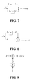
- Figures 7 to 10 show in schematic blocks the different blocks composing the memory 2 for a linear and systematic coding.
- Figure 7 shows the coding block COD located immediately downstream of the input terminal.
- the calculation of the syndrome s uses almost integrally the parity calculation circuit used for the coding COD.
- the block for decoding a single error provides a decoding circuit E, of limited complexity, proportional to the number of single errors to be corrected.
- the block E recognises each one of the 128 syndromes associated to a single error and it activates, through the vector "e", the correction of the corresponding bit.
- the vector "e" is void and the original data d is outputted.
- Figure 10 shows a simple activation block of a signal q being simultaneously activated when the intervention of the external correction is required.
- the memory system 1 uses the high parallelism being available on the reading path.
- the parallel reading of a 144-bit data page and the writing, i.e. the parallel programming of a 144-bit data page are only available for memory-integrated coding, decoding and correction solutions.
- a first error correction process relates to the determination of the syndrome "s" and to the correction of single errors, performed in the memory 2.
- memory 2 simultaneously comprises all K bits of the read page (data + parity), the calculation of the syndrome s and the single error correction can be immediately performed.
- the memory 2 immediately indicates to the controller 3, through the dedicated IRQ line, the need to perform an external correction, in this case any alteration is applied on read data.
- the controller 3 When, after a data request, the controller 3 received from the memory 2 the indication that two or more errors occurred, the normal data transfer is interrupted.
- the syndrome s calculated in the memory 2 is read. If the syndrome is associated to a double error, the locations of the wrong bits are detected, data are then read by the memory 2 and corrected where they must be corrected.
- This operation is not very frequent and more complex than the single error correction; in fact it requires more memory or calculation capacity, it can be advantageously performed by the controller without endangering system performances.
Landscapes
- Engineering & Computer Science (AREA)
- Theoretical Computer Science (AREA)
- Quality & Reliability (AREA)
- Physics & Mathematics (AREA)
- General Engineering & Computer Science (AREA)
- General Physics & Mathematics (AREA)
- Techniques For Improving Reliability Of Storages (AREA)
- Detection And Correction Of Errors (AREA)
Abstract
Description
- In its more general aspect, the present invention relates to the field of memory systems comprising at least a non volatile memory and a controller.
- Such a system can be an independent information storage unit or it can be used as a control or processing unit for a general application.
- More particularly, the invention relates to an integrated memory system comprising at least a non volatile memory and an automatic error corrector.
- In this specific technical field, it is well known that in an information storage unit (figure 2) the controller functions as interface towards the user, according to a predetermined convention, by using an interface and some services made available by the memory.
- This is the typical condition of storage systems like Disk-on-Chip, Memory Card or Smart Card, as schematised in the here-attached figure 2.
- In a general control unit (figure 3) a predetermined software level attends to providing interface functions to overhanging software levels by using said interface and services made available by the memory.
- In an ideal system, without errors, the memory receives/ sends the data sent/required by the controller without error possibility.
- In a real system, however, it is almost impossible to send and store data always without errors.
- Data Storage Flash memories use the most developed technologies to integrate most of the information per area unit. For these applications NAND, Multilevel NAND and Multilevel NOR memories are commonly used. The error probability of these memories is not void and it increases as the memory ages because of well known physical phenomena.
- For example, in a floating gate memory cell, the information storage capacity is influenced by several mechanisms as: the charge maintaining, the "read disturb" mechanism, the "program disturb" mechanism, the SILC phenomenon, having a different influence as the memory ages.
- In substance, the error probability which must be offered by the memory system is determined by the kind of application required by the user and it is usually lower than the error probability offered by Flash memories during their life span.
- A convenient memory system must provide some devices and functions to show externally, or at overhanging levels, an error probability being lower or equal to the one required by the application. This is commonly achieved by using error correction techniques.
- These error correction techniques provide that the information is split in words of K bits and that these words are conveniently coded with N bits, where R redundancy bits are added to the K information bits. Only at this point words are written in the memory.
- During the information reading, the K original information bits are decoded from the N bits read by the memory.
- The presence of R redundancy bits allows the original information to be recovered if the error number is lower than W. Different codings for the K information bit protection from W errors by coding on N bits are known in the prior art.
- For convenience of illustration, a practical case of a linear and systematic coding (144, 128) for correcting two errors (N=144 bits, K=128 bits, W=2 bits) will be considered hereinafter.
- With reference to figure 6, the coding and decoding of such a code can be summarised as follows:
- The vector "c" to be stored, composed of 144 bits, is obtained as vector product of "i", 128-bit data vector, with the binary generating matrix "G" composed of 128 rows for 144 columns. In the particular linear and systematic coding case G is composed of an identity matrix I and a parity matrix P. The vector "c" being obtained thus comprises the repetition of the data vector "i" and the parity vector is obtained as vector product iP. Formally expressed:

- The matrix P is a binary matrix of size 128 X 16 being conveniently chosen (the method for obtaining this matrix is known to the expert in the art).
- For the decoding step a so-called syndrome "s" must be calculated:


- The syndrome "s", 16-bit vector, is obtained as vector product between the vector "r", data vector of 144 bits read by the memory and composed of a 128-bit data part "d" and a 16-bit parity part "p", and the transpose of the matrix H. It can be shown that the syndrome is equivalent to the sum in GF(2) of the parity vector "p" with the vector product of the vector d with the parity matrix P.
- The syndrome s is void if the data vector "r" is correct; while, according to the way the matrix P is defined, "s" has a sole value for each possible configuration of one or two errors affecting "r".
- To achieve this coding and decoding scheme some solutions are known, which are schematically shown in figures 4a and b.
- In the first solution of figure 4a a general memory is used. This memory stores data "i" and parity bits "iP" calculated by the controller. The coding and decoding task for correcting errors is entrusted to the controller.
- The disadvantages of this solution are:
- high latency time between the data request and the availability thereof.
In fact standard Flash memories use a limited-size interface bus to communicate with the controller. Although the memory internal reading is commonly performed for pages having several bits (for example 144 bits), the communication towards the controller is bound to a word sequence on the data bus. Since for calculating the syndrome, and thus for detecting and correcting the error, all the page bits are necessary, data are available for the user only after transferring all K bit of the page (data + parity) in the controller and after calculating the parity. - a memory overhead in the controller.
In fact the K bits of the page (data + parity) must be loaded in the controller memory with subsequent occupation of a controller memory area. - an overhead in the controller processing resources.
- In fact the controller must, for each data page, read all K bits of the page (data + parity). For each page it must therefore calculate the parity and, if the latter indicates an error, activate the correction.
- For performing these operations the controller requires a calculation power overhead so as not to influence the memory system overall performances; moreover a part of the transmission band between the memory and the controller is used for transmitting parity bits being not strictly necessary for the user application.
- In this second prior art solution, shown in figure b, the coding and decoding task is entrusted to the memory. The syndrome decoding for correcting two errors is generally too onerous in terms of area to be advantageously implemented in the memory.
- The technical problem underlying the present invention is to provide an integrated memory system, having such structural and functional characteristics as to ensure an automatic error correction in data storage overcoming the drawbacks mentioned with reference to the prior art.
- The solution idea underlying the present invention provides the possibility and opportunity to split the correction in different processes to be performed directly in the memory or in the controller.
- On the basis of this solution idea the technical problem is solved by a memory system defined in the characterising part of claim 1.
- The features and advantages of the system according to the invention will be apparent from the following description of an embodiment thereof given by way of non-limiting example with reference to the attached drawings.
-
- Figure 1 is a schematic block view of a memory system incorporating at least a non volatile memory and a controller;
- Figure 2 is a schematic block view of the system of figure 1 used as information storage unit;
- Figure 3 is a schematic block view of the system of figure 1 used as control or processing unit;
- Figure 4a schematically shows a known memory system equipped with devices for the automatic error correction;
- Figure 4b schematically shows a further known memory system equipped with other devices for the automatic error correction;
- Figure 5 schematically shows a memory system according to the invention incorporating devices for the automatic error correction;
- Figure 6 is a schematic block view of a non volatile memory portion incorporated in the system of figure 5;
- Figures 7 to 10 are respective schematic block views of components of the memory of figure 6.
- With reference to the drawings, and particularly to the example of figure 5, a memory system in accordance with the present invention to store data and information in binary logic is globally and schematically indicated with 1.
- Such a system can be an independent information storage unit (figure 2) or it can be used as a control or processing unit for a general application (figure 3).
- The system 1 comprises at least a non
volatile memory 2, for example of the Flash type, and acontroller 3 associated to thememory 2 by means of aninterface bus 4. - Non volatile memories are electronic devices integrated on semiconductor and equipped with memory cell matrixes, particularly multilevel cells.
- More particularly, memory device means any monolithic electronic system incorporating a memory cell matrix, organised into rows, referred to as word lines, and columns, referred to as bit lines, as well as circuit portions associated to the cell matrix and responsible for addressing, decoding, reading, writing and erasing the memory cell content.
- Such a device can be for example a memory chip integrated on semiconductor and of the non volatile EEPROM Flash type split in sectors and electrically erasable. Each memory cell comprises a floating gate transistor with source, drain and control gate terminals.
- The memory system 1 is advantageously equipped with a particular device for the automatic correction of storage errors.
- In particular, the system 1 provides the possibility and opportunity to split the correction in different processes to be performed directly in the
memory 2 or in thecontroller 3. - As shown in figure 6, the structure of the memory system 1 is composed of a set of functional blocks located between an input terminal In and an output terminal Out.
-
Memory 2 comprises, besidesrespective areas - circuits COD for the coding required to correct two errors;
- a logic SYND for calculating the syndrome s;
- a circuit COR for correcting a single error;
- a logic Ext COR for detecting more than one error;
- a
logic 4 for bringing to the controller 3: - a one-or-no-error-corrected data ;
- the uncorrected error;
- the calculated syndrome s;
- a signal IRQ activated to request the external correction.
- Figures 7 to 10 show in schematic blocks the different blocks composing the
memory 2 for a linear and systematic coding. - Figure 7 shows the coding block COD located immediately downstream of the input terminal.
- The vector product iP, performed by the block P, has a limited circuit complexity, proportional to the number of parity bits, and it is obtained through the synthesis of the corresponding logic function: c=[i, iP].
- Figure 8 shows the block SYND for calculating the syndrome s=p+dP.
- The calculation of the syndrome s uses almost integrally the parity calculation circuit used for the coding COD.
- Figure 9 shows the block COR for correcting one error and the block for requiring the external correction Ext COR with o=d+e.
- The block for decoding a single error provides a decoding circuit E, of limited complexity, proportional to the number of single errors to be corrected.
- This block is obtained through synthesis of the functional description thereof. In practise, the block E recognises each one of the 128 syndromes associated to a single error and it activates, through the vector "e", the correction of the corresponding bit.
- If there are no errors to be corrected (s=0) or the syndrome value does not belong to the set of single errors, the vector "e" is void and the original data d is outputted.
- Figure 10 shows a simple activation block of a signal q being simultaneously activated when the intervention of the external correction is required.
- The memory system 1 according to the invention, incorporating the previously mentioned correction blocks, uses the high parallelism being available on the reading path. In fact, the parallel reading of a 144-bit data page and the writing, i.e. the parallel programming of a 144-bit data page, are only available for memory-integrated coding, decoding and correction solutions.
- The operating method of the memory system according to the invention will now be described.
- A first error correction process relates to the determination of the syndrome "s" and to the correction of single errors, performed in the
memory 2. - These functions are sufficiently simple and little onerous from a circuit point of view so as to be advantageously performed in the
memory 2. - Since
memory 2 simultaneously comprises all K bits of the read page (data + parity), the calculation of the syndrome s and the single error correction can be immediately performed. - This allows the corrected data to be transferred to the
controller 3, immediately and with void latency, with no need to transfer also the parity. Therefore the Bus band for the parity transfer is not occupied. - If several errors occur, the
memory 2 immediately indicates to thecontroller 3, through the dedicated IRQ line, the need to perform an external correction, in this case any alteration is applied on read data. - The correction of all double errors, performed by the controller, will now be described.
- When, after a data request, the
controller 3 received from thememory 2 the indication that two or more errors occurred, the normal data transfer is interrupted. - The syndrome s calculated in the
memory 2 is read. If the syndrome is associated to a double error, the locations of the wrong bits are detected, data are then read by thememory 2 and corrected where they must be corrected. - This operation is not very frequent and more complex than the single error correction; in fact it requires more memory or calculation capacity, it can be advantageously performed by the controller without endangering system performances.
- Other particular cases will now be described:
- 1) The correction of more than two errors indicated by the syndrome s (Controller or user SW)
If the syndrome calculated in the memory is not associated to any error, neither single nor double, it serves as a detector of three or more errors.
The capacity of detecting all or a part of higher order errors (3, 4, ...) exclusively depends on the chosen parity matrix. The detection of a higher order error (i.e. higher than 2) allows thecontroller 3 to use this information to activate the decoding of a correction code at a higher software level, on the same set of data or on a larger size set.
The single errors being already corrected inside the memory and double errors being already corrected through the parity calculated in the memory, the events with three or more errors are extremely rare and, although the correction thereof is complex, they do not significantly affect system performances.
Thecontroller 3 overhead is limited to the correction of two errors, when explicitly required by the indication from the memory and it is limited to the reading of the syndrome s, calculated in the memory, and to the correction of double errors.
If the probability to have an error in a 128-bit page is for example 10-5, the probability to have two errors is about 10-10, the number of interventions by thecontroller 3 is therefore reduced by five quantities. The probability to have more than two errors is about 10-15 and thus extremely improbable.
When required by the memory, through the IRQ signal, the controller provides to:- reading the syndrome s
- calculating the two bits to be redounded through one of the following two methods:
- searching, on an ordered table, the syndromes of two errors. This method requires an ordered table of the N(N-1) syndromes associated to two wrong bits and a number of operations equal to O(Nlog N).
- 2) Comparing all the syndromes obtainable as sum of two rows of the parity P matrix.
- If the search detects the couple of wrong bits, the data reading, the correction thereof and the transmission to the user are performed.
- If the search does not detect the couple of wrong bits, this means that the syndrome indicates the presence of three or more errors. The controller or driver SW asks the higher SW levels to correct these errors.
- It will be evident to the expert in the art how to apply the error correction devices according to the present invention also to other circuit solutions allowing a split of the single error correction functions. For example the principles of the present invention can be applied also when the error correction system is taken from the memory and integrated in a coprocessor or in an accelerator in the control unit.
Claims (8)
- An integrated memory system (1), comprising at least a non volatile memory (2) and an automatic storage error corrector (3), characterised in that it comprises circuit means, functionally independent, each of them being responsible for the correction of a predetermined storage error; at least one of said means generating a signal (IRQ) to ask a correction being external to the memory (2).
- A system according to claim 1, characterised in that said memory (2) is connected to a controller (3) by means of an interface bus (4) and in that said means are incorporated both in the memory (2) and in the controller (3).
- A system according to claim 1, characterised in that in the memory (2) said means comprise at least:- circuits (COD) for the coding required to correct two errors;- a logic (SYND) for calculating the syndrome (s);- a circuit (COR) for correcting a single error;- a logic (Ext COR) for detecting more than one error.
- A system according to claim 3, characterised in that said means also comprise:- a logic for bringing to the controller (3):- a one-or-no-error-corrected data ;- the uncorrected error;- the calculated syndrome (s);
- A system according to claim 2, characterised in that said means comprise a circuit for generating a signal (IRQ) activated to request the external correction of an error by said controller (3).
- A system according to claim 3, characterised in that said coding block (COD) is located immediately downstream of the input terminal of said memory (2) and it performs a vector product (iP) proportional to the number of parity bits and obtained through the synthesis of a corresponding logic function: c=[i, iP].
- A system according to claim 6, characterised in that said logic (SYND) for calculating the syndrome (s) uses again the parity calculation circuit of the coding block (COD).
- A system according to claim 3, characterised in that said circuit (COR) for correcting a single error comprises a block (E) for decoding a single error effective to recognise each of the several syndromes (s) associated to a single error to activate, through a corresponding vector (e), the correction of the corresponding bit.
Priority Applications (2)
| Application Number | Priority Date | Filing Date | Title |
|---|---|---|---|
| EP03425171.0A EP1460542B1 (en) | 2003-03-19 | 2003-03-19 | Integrated memory system comprising at least a non-volatile memory and an automatic error corrector |
| US10/805,182 US7730357B2 (en) | 2003-03-19 | 2004-03-19 | Integrated memory system |
Applications Claiming Priority (1)
| Application Number | Priority Date | Filing Date | Title |
|---|---|---|---|
| EP03425171.0A EP1460542B1 (en) | 2003-03-19 | 2003-03-19 | Integrated memory system comprising at least a non-volatile memory and an automatic error corrector |
Publications (2)
| Publication Number | Publication Date |
|---|---|
| EP1460542A1 true EP1460542A1 (en) | 2004-09-22 |
| EP1460542B1 EP1460542B1 (en) | 2018-10-31 |
Family
ID=32799218
Family Applications (1)
| Application Number | Title | Priority Date | Filing Date |
|---|---|---|---|
| EP03425171.0A Expired - Lifetime EP1460542B1 (en) | 2003-03-19 | 2003-03-19 | Integrated memory system comprising at least a non-volatile memory and an automatic error corrector |
Country Status (2)
| Country | Link |
|---|---|
| US (1) | US7730357B2 (en) |
| EP (1) | EP1460542B1 (en) |
Families Citing this family (2)
| Publication number | Priority date | Publication date | Assignee | Title |
|---|---|---|---|---|
| JP4564520B2 (en) | 2007-08-31 | 2010-10-20 | 株式会社東芝 | Semiconductor memory device and control method thereof |
| US8904250B2 (en) * | 2013-02-14 | 2014-12-02 | Micron Technology, Inc. | Autorecovery after manufacturing/system integration |
Citations (2)
| Publication number | Priority date | Publication date | Assignee | Title |
|---|---|---|---|---|
| US5922080A (en) | 1996-05-29 | 1999-07-13 | Compaq Computer Corporation, Inc. | Method and apparatus for performing error detection and correction with memory devices |
| JP2001175542A (en) | 1999-12-16 | 2001-06-29 | Hitachi Ltd | Recording / reproducing device and semiconductor memory |
Family Cites Families (8)
| Publication number | Priority date | Publication date | Assignee | Title |
|---|---|---|---|---|
| US5533035A (en) * | 1993-06-16 | 1996-07-02 | Hal Computer Systems, Inc. | Error detection and correction method and apparatus |
| US7134069B1 (en) * | 1999-06-16 | 2006-11-07 | Madrone Solutions, Inc. | Method and apparatus for error detection and correction |
| CN1286275C (en) * | 1999-11-24 | 2006-11-22 | 三洋电机株式会社 | Debugging device |
| FR2810152A1 (en) * | 2000-06-13 | 2001-12-14 | St Microelectronics Sa | EEPROM for securing electronic devices such as chip cards has elements for detection and correction of memory errors within the secure non-erasable memory area |
| US6745310B2 (en) * | 2000-12-01 | 2004-06-01 | Yan Chiew Chow | Real time local and remote management of data files and directories and method of operating the same |
| US20020174397A1 (en) * | 2001-05-16 | 2002-11-21 | Fujitsu Limited | Method for error detection/correction of multilevel cell memory and multilevel cell memory having error detection/correction function |
| US6996741B1 (en) * | 2001-11-15 | 2006-02-07 | Xiotech Corporation | System and method for redundant communication between redundant controllers |
| US20040015771A1 (en) * | 2002-07-16 | 2004-01-22 | Menahem Lasser | Error correction for non-volatile memory |
-
2003
- 2003-03-19 EP EP03425171.0A patent/EP1460542B1/en not_active Expired - Lifetime
-
2004
- 2004-03-19 US US10/805,182 patent/US7730357B2/en not_active Expired - Lifetime
Patent Citations (2)
| Publication number | Priority date | Publication date | Assignee | Title |
|---|---|---|---|---|
| US5922080A (en) | 1996-05-29 | 1999-07-13 | Compaq Computer Corporation, Inc. | Method and apparatus for performing error detection and correction with memory devices |
| JP2001175542A (en) | 1999-12-16 | 2001-06-29 | Hitachi Ltd | Recording / reproducing device and semiconductor memory |
Non-Patent Citations (1)
| Title |
|---|
| PATENT ABSTRACTS OF JAPAN vol. 2000, no. 23 10 February 2001 (2001-02-10) * |
Also Published As
| Publication number | Publication date |
|---|---|
| US20040230869A1 (en) | 2004-11-18 |
| US7730357B2 (en) | 2010-06-01 |
| EP1460542B1 (en) | 2018-10-31 |
Similar Documents
| Publication | Publication Date | Title |
|---|---|---|
| US7403436B2 (en) | Non-volatile semiconductor memory device | |
| US8954818B2 (en) | Error detection and correction scheme for a memory device | |
| US8239725B2 (en) | Data storage with an outer block code and a stream-based inner code | |
| EP0704854B1 (en) | Memory device having error detection and correction function, and methods for writing and erasing the memory device | |
| EP1416380A2 (en) | Method and apparatus for managing the integrity of data in a non-volatile memory system | |
| JP3982639B2 (en) | Method for reading data from a memory having multi-level cells | |
| US7644342B2 (en) | Semiconductor memory device | |
| US7809994B2 (en) | Error correction coding for multiple-sector pages in flash memory devices | |
| KR101138120B1 (en) | Chien search device and chien search method | |
| US20070300130A1 (en) | Method of Error Correction Coding for Multiple-Sector Pages in Flash Memory Devices | |
| EP2186004B1 (en) | Semiconductor memory device and method of controlling the same | |
| TWI768511B (en) | Data accessing method using data protection with aid of parity check matrix having partial sequential information, and associated apparatus | |
| JP2000305861A (en) | Storage device and memory card | |
| EP0383899B1 (en) | Failure detection for partial write operations for memories | |
| EP1460542B1 (en) | Integrated memory system comprising at least a non-volatile memory and an automatic error corrector | |
| US20250370858A1 (en) | Non-volatile memory metadata protection | |
| JP3482543B2 (en) | Semiconductor memory | |
| US11971775B2 (en) | Predicting an unsuccessful error correction code condition using a dynamic read threshold table | |
| CN119694374B (en) | Memory devices, memory systems and their operating methods, storage media | |
| SU922868A1 (en) | PERMANENT STORAGE DEVICE 1 | |
| SU1111205A1 (en) | Storage with error correction | |
| JP2007179480A (en) | Memory controller and flash memory system |
Legal Events
| Date | Code | Title | Description |
|---|---|---|---|
| PUAI | Public reference made under article 153(3) epc to a published international application that has entered the european phase |
Free format text: ORIGINAL CODE: 0009012 |
|
| AK | Designated contracting states |
Kind code of ref document: A1 Designated state(s): AT BE BG CH CY CZ DE DK EE ES FI FR GB GR HU IE IT LI LU MC NL PT RO SE SI SK TR |
|
| AX | Request for extension of the european patent |
Extension state: AL LT LV MK |
|
| 17P | Request for examination filed |
Effective date: 20050317 |
|
| AKX | Designation fees paid |
Designated state(s): DE FR GB IT |
|
| 17Q | First examination report despatched |
Effective date: 20080818 |
|
| RAP1 | Party data changed (applicant data changed or rights of an application transferred) |
Owner name: STMICROELECTRONICS SRL |
|
| RAP1 | Party data changed (applicant data changed or rights of an application transferred) |
Owner name: STMICROELECTRONICS SRL |
|
| RAP1 | Party data changed (applicant data changed or rights of an application transferred) |
Owner name: MICRON TECHNOLOGY, INC. |
|
| GRAP | Despatch of communication of intention to grant a patent |
Free format text: ORIGINAL CODE: EPIDOSNIGR1 |
|
| INTG | Intention to grant announced |
Effective date: 20180514 |
|
| GRAS | Grant fee paid |
Free format text: ORIGINAL CODE: EPIDOSNIGR3 |
|
| GRAA | (expected) grant |
Free format text: ORIGINAL CODE: 0009210 |
|
| AK | Designated contracting states |
Kind code of ref document: B1 Designated state(s): DE FR GB IT |
|
| REG | Reference to a national code |
Ref country code: GB Ref legal event code: FG4D |
|
| REG | Reference to a national code |
Ref country code: DE Ref legal event code: R096 Ref document number: 60351590 Country of ref document: DE |
|
| RIC2 | Information provided on ipc code assigned after grant |
Ipc: G06F 11/10 20060101AFI20030930BHEP |
|
| PG25 | Lapsed in a contracting state [announced via postgrant information from national office to epo] |
Ref country code: IT Free format text: LAPSE BECAUSE OF FAILURE TO SUBMIT A TRANSLATION OF THE DESCRIPTION OR TO PAY THE FEE WITHIN THE PRESCRIBED TIME-LIMIT Effective date: 20181031 |
|
| REG | Reference to a national code |
Ref country code: DE Ref legal event code: R097 Ref document number: 60351590 Country of ref document: DE |
|
| PLBE | No opposition filed within time limit |
Free format text: ORIGINAL CODE: 0009261 |
|
| STAA | Information on the status of an ep patent application or granted ep patent |
Free format text: STATUS: NO OPPOSITION FILED WITHIN TIME LIMIT |
|
| 26N | No opposition filed |
Effective date: 20190801 |
|
| PGFP | Annual fee paid to national office [announced via postgrant information from national office to epo] |
Ref country code: GB Payment date: 20220322 Year of fee payment: 20 |
|
| PGFP | Annual fee paid to national office [announced via postgrant information from national office to epo] |
Ref country code: FR Payment date: 20220325 Year of fee payment: 20 |
|
| PGFP | Annual fee paid to national office [announced via postgrant information from national office to epo] |
Ref country code: DE Payment date: 20220428 Year of fee payment: 20 |
|
| REG | Reference to a national code |
Ref country code: DE Ref legal event code: R071 Ref document number: 60351590 Country of ref document: DE |
|
| REG | Reference to a national code |
Ref country code: GB Ref legal event code: PE20 Expiry date: 20230318 |
|
| PG25 | Lapsed in a contracting state [announced via postgrant information from national office to epo] |
Ref country code: GB Free format text: LAPSE BECAUSE OF EXPIRATION OF PROTECTION Effective date: 20230318 |