EP1458108A1 - Dual resonance antenna apparatus - Google Patents
Dual resonance antenna apparatus Download PDFInfo
- Publication number
- EP1458108A1 EP1458108A1 EP02786142A EP02786142A EP1458108A1 EP 1458108 A1 EP1458108 A1 EP 1458108A1 EP 02786142 A EP02786142 A EP 02786142A EP 02786142 A EP02786142 A EP 02786142A EP 1458108 A1 EP1458108 A1 EP 1458108A1
- Authority
- EP
- European Patent Office
- Prior art keywords
- circuit
- antenna
- antenna device
- resonant
- frequency
- Prior art date
- Legal status (The legal status is an assumption and is not a legal conclusion. Google has not performed a legal analysis and makes no representation as to the accuracy of the status listed.)
- Granted
Links
Images





Classifications
-
- H—ELECTRICITY
- H01—ELECTRIC ELEMENTS
- H01Q—ANTENNAS, i.e. RADIO AERIALS
- H01Q5/00—Arrangements for simultaneous operation of antennas on two or more different wavebands, e.g. dual-band or multi-band arrangements
-
- H—ELECTRICITY
- H04—ELECTRIC COMMUNICATION TECHNIQUE
- H04B—TRANSMISSION
- H04B1/00—Details of transmission systems, not covered by a single one of groups H04B3/00 - H04B13/00; Details of transmission systems not characterised by the medium used for transmission
- H04B1/02—Transmitters
- H04B1/04—Circuits
- H04B1/0458—Arrangements for matching and coupling between power amplifier and antenna or between amplifying stages
-
- H—ELECTRICITY
- H01—ELECTRIC ELEMENTS
- H01Q—ANTENNAS, i.e. RADIO AERIALS
- H01Q21/00—Antenna arrays or systems
- H01Q21/30—Combinations of separate antenna units operating in different wavebands and connected to a common feeder system
-
- H—ELECTRICITY
- H01—ELECTRIC ELEMENTS
- H01Q—ANTENNAS, i.e. RADIO AERIALS
- H01Q5/00—Arrangements for simultaneous operation of antennas on two or more different wavebands, e.g. dual-band or multi-band arrangements
- H01Q5/30—Arrangements for providing operation on different wavebands
- H01Q5/307—Individual or coupled radiating elements, each element being fed in an unspecified way
- H01Q5/314—Individual or coupled radiating elements, each element being fed in an unspecified way using frequency dependent circuits or components, e.g. trap circuits or capacitors
- H01Q5/335—Individual or coupled radiating elements, each element being fed in an unspecified way using frequency dependent circuits or components, e.g. trap circuits or capacitors at the feed, e.g. for impedance matching
-
- H—ELECTRICITY
- H04—ELECTRIC COMMUNICATION TECHNIQUE
- H04B—TRANSMISSION
- H04B1/00—Details of transmission systems, not covered by a single one of groups H04B3/00 - H04B13/00; Details of transmission systems not characterised by the medium used for transmission
- H04B1/005—Details of transmission systems, not covered by a single one of groups H04B3/00 - H04B13/00; Details of transmission systems not characterised by the medium used for transmission adapting radio receivers, transmitters andtransceivers for operation on two or more bands, i.e. frequency ranges
-
- H—ELECTRICITY
- H04—ELECTRIC COMMUNICATION TECHNIQUE
- H04B—TRANSMISSION
- H04B1/00—Details of transmission systems, not covered by a single one of groups H04B3/00 - H04B13/00; Details of transmission systems not characterised by the medium used for transmission
- H04B1/005—Details of transmission systems, not covered by a single one of groups H04B3/00 - H04B13/00; Details of transmission systems not characterised by the medium used for transmission adapting radio receivers, transmitters andtransceivers for operation on two or more bands, i.e. frequency ranges
- H04B1/0053—Details of transmission systems, not covered by a single one of groups H04B3/00 - H04B13/00; Details of transmission systems not characterised by the medium used for transmission adapting radio receivers, transmitters andtransceivers for operation on two or more bands, i.e. frequency ranges with common antenna for more than one band
- H04B1/0057—Details of transmission systems, not covered by a single one of groups H04B3/00 - H04B13/00; Details of transmission systems not characterised by the medium used for transmission adapting radio receivers, transmitters andtransceivers for operation on two or more bands, i.e. frequency ranges with common antenna for more than one band using diplexing or multiplexing filters for selecting the desired band
-
- H—ELECTRICITY
- H03—ELECTRONIC CIRCUITRY
- H03H—IMPEDANCE NETWORKS, e.g. RESONANT CIRCUITS; RESONATORS
- H03H7/00—Multiple-port networks comprising only passive electrical elements as network components
- H03H7/38—Impedance-matching networks
- H03H2007/386—Multiple band impedance matching
Definitions
- the present invention relates to a multi-resonant antenna device which is made to resonate in a plurality of frequency bands and more particularly to an improvement in the gain of a multi-resonant antenna device.
- circuit construction shown in Fig. 10 or Fig. 11 is adopted in order to realize a multi-resonant antenna device resonating in two frequency bands, for example (see "Antenna Engineering Handbook", pp. 44-45, compiled by The Institute of Electronics, Information and Communication Engineers and published by Ohmsha on Oct. 30, 1981).
- a multi-resonant antenna device 1 shown in Fig. 10 one antenna element 2 is used and power is supplied to the antenna element 2 from a power supply circuit 3 through one feeding point 4.
- an inductance element 5 and capacitance elements 7 and 8 are connected to constitute an LC parallel resonance circuit 9. More concretely, the inductance element 5 and the capacitance element 7 are connected in series between the antenna element 2 and the power supply circuit 3. The capacitance element 8 is connected in parallel with the series circuit of the inductance element 5 and the capacitance element 7.
- an inductance element 6 is connected between the feeding point 4 and ground. This inductance element 6 is to match the input impedance of the antenna element 2 with the impedance of the power supply circuit 3.
- a multi-resonant antenna device 11 shown in Fig. 11 two antenna elements 12 and 13 are used. Power is supplied to the antenna elements 12 and 13 from a power supply circuit 14 through a feeding point 15.
- An inductance element 16 is connected between the antenna element 12 and the power supply circuit 14, and a capacitance element 18 is connected between the antenna element 13 and the power supply circuit 14. Furthermore, an inductance element 17 is connected between the feeding point 15 and ground. The inductance element 17 is to match the input impedance of the antenna elements 12 and 13 with the impedance of the power supply circuit 14.
- the multi-resonant antenna device 11 is made to resonate in two frequency bands such that the resonance frequency of each of the antenna elements 12 and 13 is matched to a desired frequency band.
- the multi-resonant antenna devices 1 and 11 shown in Figs. 10 and 11 have the following problem.
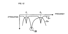
- Fig. 12 shows the reflection frequency characteristic S 11 and transmission frequency characteristic S 21 of the multi-resonant antenna device 1 and 11. In Fig. 12, two resonance frequencies f 1 and f 2 are shown.
- the LC parallel resonance circuit 9 has an antiresonant frequency which is determined by the inductance component and capacitance components contained therein and the impedance becomes infinite at that frequency.
- a drop in the gain, that is, a notch portion 20 appears between the two resonance frequencies f 1 and f 2 in the transmission characteristic S 21 .
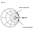
- Fig. 13 is a Smith chart showing the impedance frequency characteristic (S 11 ) of the LC parallel resonance circuit 9 shown in Fig. 10.
- the impedance frequency characteristic (S 11 ) of the LC parallel resonance circuit 9 is shown by a circular locus extending from an inductive point to a capacitive point on the Smith chart, as shown in Fig. 13. That is, the frequency characteristic is inductive in the 800 MHz band, that is, the locus is on the upper side of the Smith chart, and the frequency characteristic is capacitive in the 1.5 GHz band, that is, the locus is on the lower side of the Smith chart.
- the multi-resonant antenna device 11 shown in Fig. 11 since the two antenna elements 12 and 13 are disposed close to each other, those antenna elements 12 and 13 are capacitively coupled and a parallel resonance circuit is formed due to the capacitance and inductance components contained in the antenna elements 12 and 13.
- This parallel resonance circuit has the same construction as in the LC parallel resonance circuit 9 shown in Fig. 10, and accordingly, also in the case of the multi-resonant antenna device 11 shown in Fig. 11, the notch portion 20, indicating the drop in gain, appears between the two resonance frequencies f 1 and f 2 in the transmission characteristics S 21 , as shown in Fig. 12, which is the same as in the multi-resonant antenna device 1 shown in Fig. 10.
- Such a notch portion 20 becomes the cause of deterioration of the gain and accordingly it must be eliminated.
- multi-resonant antenna device there are an antenna device of a first embodiment in which one antenna element is used and an antenna device of a second embodiment in which two antenna elements are used.
- the multi-resonant antenna device comprises an antenna element and an LC resonance circuit making the antenna element resonate in a plurality of frequency bands.
- the LC resonant circuit contains a T-type circuit or PI-type circuit, composed of an inductance element and a capacitance element, for preventing the impedance from becoming infinite in a certain frequency band.
- the LC resonance circuit further contains a diode switching circuit connected in parallel with the T-type circuit or PI-type circuit and the antenna element may be made to resonate in three or more frequency bands by turning on and off the diode switching circuit.
- the multi-resonant antenna device comprises two antenna elements resonating in a plurality of frequency bands.
- a T-type circuit or PI-type circuit composed of an inductance element and a capacitance element, for preventing the impedance from becoming infinite in a certain frequency band, is contained between at least one of the antenna elements and a feeding point.
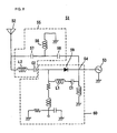
- Fig. 1 is a circuit diagram of a multi-resonant antenna device 21 according to a first embodiment of the present invention.
- the multi-resonant antenna device 21 contains one antenna element 22 and power is supplied to the antenna element 22 from a power supply circuit 23 through one feeding point 24.
- inductance elements 25 and 26 and capacitance elements 28, 29, and 30 are connected to constitute an LC parallel resonance circuit 31. More concretely, between the antenna element 22 and the power supply circuit 23, the inductance element 25 and the capacitance element 28 are connected in series to constitute an LC series circuit. Then, a T-type circuit composed of the capacitance elements 29 and 30 and the inductance element (inductor) 26 as a shunt element is connected in parallel with the series circuit composed of the inductance element 25 and the capacitance element 28.
- an inductance element 27 is connected between the feeding point 24 and ground.
- the inductance element 27 functions as a matching element for matching the input impedance of the antenna element 22 to the impedance of the power supply circuit 23.
- this LC resonance circuit 31 contains an LC series circuit composed of the inductance element 25 and the capacitance element 28 and a parallel resonance circuit composed of the capacitance elements 29 and 30 connected in parallel to the LC series circuit, and also contains a T-type circuit composed of the capacitance elements 29 and 30 and the inductance element 26 (hereinafter, the LC parallel circuit may be called an LC parallel resonance circuit).
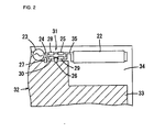
- Fig. 2 shows how the antenna element 22, which is formed of a chip antenna, is mounted.
- a grounding conductive film 33 shown by hatching is formed on a mounting board (mother board) 32 for mounting the antenna element 22.
- a part of the outer area of the grounding conductive film 33 is cut away and a rectangular conductive-film cutaway area 34 is formed in a corner portion of the mounting board 32.
- the antenna element 22 is mounted in the conductive-film cutaway area 34 on the mounting board 32.
- Fig. 2 also shows how the gain-deterioration-prevention LC circuit 31, to be connected to the above antenna element 22, is mounted.
- a wiring conductive film 35 is formed in the conductive-film cutaway area 34 on the mounting board 32, and chip parts such as chip inductors, chip capacitors, etc. constituting the above-mentioned inductance elements 25, 26, and 27 and capacitance elements 28, 29, and 30 are mounted so as to be electrically connected to the wiring conductive film 35 and, when required, to be electrically connected to the grounding conductive film 33.
- chip parts such as chip inductors, chip capacitors, etc. constituting the above-mentioned inductance elements 25, 26, and 27 and capacitance elements 28, 29, and 30 are mounted so as to be electrically connected to the wiring conductive film 35 and, when required, to be electrically connected to the grounding conductive film 33.
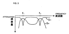
- Fig. 3 which corresponds to Fig. 12, shows the reflection frequency characteristic S 11 and transmission frequency characteristic S 21 of the multi-resonant antenna device 21.
- the multi-resonant antenna device 21 has two resonance frequencies f 1 and f 2 , no drop in gain, that is, no notch portion, is caused between the two resonance frequencies f 1 and f 2 in the frequency characteristic S 21 .
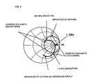
- Fig. 4 is a Smith chart showing the impedance frequency characteristic (S 11 ) of the LC resonance circuit 31 shown in Fig. 1.
- the impedance frequency characteristic (S 11 ) of the LC parallel resonance circuit 31 is shown as a circular locus extending from an inductive point to a capacitive point on the Smith chart, as shown by a thick solid line in Fig. 4. That is, the impedance is inductive in the 800 MHz band on the upper side of the Smith chart and the impedance is capacitive in the 1.5 GHz band on the lower side of the Smith chart. This fact is the same as in the case of the LC resonance circuit 9 shown as related art in Fig. 10.
- the multi-resonant antenna device 21 shown in Fig. 1 does not have any notch portion 20, showing the drop in gain, between the two frequencies f 1 and f 2 in the transmission characteristic S 21 .
- the impedance frequency characteristics (S 11 ) of the antenna element 22 is shown by a thick broken line in Fig. 4.
- the impedance frequency characteristic (S 11 ) of the open-ended antenna element 22 is shown by a circular locus extending from a capacitive point to an inductive point.
- the frequency characteristics can be made complex conjugates, that is, the circular locus can be positioned so as to be symmetrical about the horizontal line in the 800 MHz band and the 1.5 GHz band, and thus matching, that is, resonance, can be achieved at each frequency.
- a multi-resonant antenna device which resonates in the two frequency bands for EPDC800 (800 MHz band) and PDC1500 (1.5 GHz band) is taken as an example and described.
- the LC resonance circuit 31 is constructed so as to be inductive in the 850 MHz band and capacitive in the 1.5 GHz band.
- the LC parallel resonance circuit 31 is constructed so that there is no antiresonant frequency where the impedance becomes infinite, the LC circuit 31 is inductive and capacitive in the two frequency bands respectively, and the LC circuit 31 resonates in these two frequency bands, the notch portion can be prevented, as described above.
- Table 1 shows the typical frequency characteristics of the multi-resonant antenna device 21 shown in Fig. 1
- Table 2 shows the typical frequency characteristics of the multi-resonant antenna device 1 shown in Fig. 10.
- Fig. 5 shows the circuit diagram of a multi-resonant antenna device 41 according to a second embodiment of the present invention.
- the multi-resonant antenna device 41 contains two antenna elements 42 and 43. These multi-resonant antenna devices 42 and 43 used have different resonant frequencies from each other, 800 MHz and 1.5 GHz, for example. Power is supplied to the antenna elements 42 and 43 from a power supply circuit 44 through one feeding point 45.
- two capacitance elements 48 and 49 are connected in series and an inductor 46 as a shunt element is connected between the middle point of the capacitance elements 48 and 49 and ground, and thus a T-type LC circuit 50 composed of the capacitance elements 48 and 49 and the inductance element 46 is constructed.
- an inductance element 47 is connected between the feeding point 45 and ground. This inductance element 47 is to match the input impedance of the antenna elements 42 and 43 to the impedance of the power supply circuit 44.
- a chip antenna can be used and, when such a chip antenna is used, the antenna elements 42 and 43 can be mounted as shown in Fig. 6. That is, the antenna elements 42 and 43 can be mounted in the conductive-film cutaway area 34 on the mounting board 32 so as to be parallel.
- Fig. 6 shows how the T-type LC circuit 50, to be connected to the above antenna elements 42 and 43, and the inductance element 47 are mounted.
- a wiring conductive film 36 is formed and chip parts forming each of the inductance elements 46 and 47 and the capacitance elements 48 and 49 are mounted so as to be electrically connected to the wiring conductive film 36 and, when required, so as to be electrically connected to the grounding conductive film 33.
- the T-type LC circuit 50 constructed as described above is provided, it is possible to prevent the occurrence of a notch portion between the resonance frequency f 1 of the antenna element 42 and the resonance frequency f 2 of the antenna element 43 in the same way as in the case of the characteristics shown in Fig. 3. This will be described in detail below.
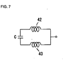
- a parallel resonance circuit is formed by the inductance component of the antenna 42, the inductance component of the antenna 43, and a capacitance due to the capacitance coupling between them.
- a frequency where the impedance becomes infinite exists in the same way as in the case of the LC parallel resonance circuit 9 shown as a related art in Fig. 10, which causes a notch portion.
- the T-type LC circuit 50 shown in Fig. 5 is inserted between at least one of the antenna elements 42 and 43 and the power supply circuit 44, there will be no frequency at which the impedance becomes infinite in the same way as described with reference to Fig. 4 in the first embodiment, and accordingly it is possible to eliminate a notch portion between the resonance frequency f 1 of the antenna element 41 and the resonance frequency f 2 of the antenna element 42.
- Table 3 shows the typical frequency characteristics of the multi-resonant antenna device 41 shown in Fig. 5
- Table 4 shows the typical frequency characteristics of the multi-resonant antenna device 11 shown in Fig. 11.
- either of the capacitance elements 29 and 30 may be replaced with an inductance element and the inductance element 25 may be replaced with a capacitance element.
- a PI-type circuit may be constructed such that another inductance element is provided as a shunt element between the inductance element 25 and the inductance element 26 so as to sandwich the capacitance element 29.
- the same can also applies to the multi-resonant antenna device 41 shown in Fig. 5.
- Fig. 8 is a circuit diagram of a multi-resonant antenna device 51 according to a third embodiment of the present invention.
- the multi-resonant antenna device 51 contains one antenna element 52 and power is supplied to the antenna element 52 from a power supply circuit 53 through one feeding point 54.
- the multi-resonant antenna device 51 is provided with an LC parallel resonance circuit 55 for preventing deterioration of the gain of the antenna element 52.
- the LC parallel resonance circuit 55 contains an inductance element 56 and capacitance elements 57 and 58, and a T-type circuit is composed of the inductance element 56, acting as a shunt element, and the capacitance elements 57 and 58 connected in series to the antenna element 52.
- This embodiment is characterized in that a diode switching circuit 60 including a diode 59 is further contained in the multi-resonant antenna device 51.
- the diode switching circuit 60 is inserted between a series circuit of the inductance element L2 and the capacitance element C2, which are contained in the LC parallel resonance circuit 55, and the power supply circuit 53 and is connected in parallel with the T-type circuit of the inductance element 56 and the capacitance elements 57 and 58, which are contained in the LC parallel resonance circuit 55.
- the diode switching circuit 60 is for increasing the number of resonant frequency bands.
- the switching between the 800 MHz-digital band (810 to 843 MHz) and the 800 MHz-analog band (870 to 885 MHz) of EPDC800 can be achieved by turning on and off the diode switching circuit 60 and, as a result, the multi-resonant antenna device 51 can cope with three different frequency bands, for example, the 800 MHz-digital band, the 800 MHz-analog band, and the 1.5 GHz band.
- the diode switching circuit 60 While the diode switching circuit 60 is turned on, the diode is short-circuited to reduce the impedance. At this time, practically no current flows in the inductance element L 1 and the capacitance element C 1 provided in the diode switching circuit 60. Therefore, it is practically the same as the condition in which there is no diode switching circuit 60, and accordingly, resonance can be achieved in both the 800 MHz-analog band and the 1.5 GHz band.
- the diode switching circuit 60 is turned off, the diode 59 is open-circuited to increase the impedance. At this time, current flows to the side with the inductance element L 1 and the capacitance element C 1 provided in the diode switching circuit 60. Therefore, the inductance component of the inductance element L 1 and the capacitance component of the capacitance element C 1 are added to the inductance component of the inductance element L 2 and the capacitance component of the capacitance element C 2 in the LC parallel resonance circuit 55, respectively, and, as a result, the characteristic value of each element in the LC parallel resonance circuit 55 changes and thus resonance is achieved in the 800 MHz-digital band.
- the LC parallel resonance circuit 55 including a T-type circuit composed of the inductance element 56 and the capacitance elements 57 and 58 is provided, the drop in gain, that is, the notch portion, can be eliminated.
- a chip antenna can be used.
- the antenna element 52 can be mounted as shown in Fig. 9. That is, the antenna element 52 can be mounted in the conductive-film cutaway area 34 on the mounting board 32.
- a wiring conductive film 37 is formed and a module chip 38, in which the above-described LC parallel resonance circuit 55, the diode switching circuit 60, etc., are integrated, is mounted so as to be electrically connected to the wiring conductive film 37 and the grounding conductive film 33.
- the module chip 38 may be replaced with the plurality of chip parts shown in Figs. 2 and 6.
- the multi-resonant antenna device for EPDC800 and PDC1500 is described, but the antenna device is not limited to that and, for example, other combinations such as EPDC800 and GPS, EPDC800 and PHS, etc., can be utilized.
- the antenna element can be made to resonate in three or more frequency bands by turning on and off the diode switching circuit.
- a multi-resonant antenna device is realized by using two antenna elements, since two antenna elements for achieving resonance in a plurality of frequency bands are used and a T-type circuit or PI-type circuit composed of an inductance element and a capacitance element, which prevents the impedance from becoming infinite in a certain frequency band, is provided between at least one of the antenna elements and a feeding point, the drop in gain that is, the notch portion, can be eliminated and deterioration of the gain can be prevented.
- a multi-resonant antenna device of the present invention which is made to resonate in a plurality of frequency bands, is used for radio communication devices such as portable telephones, etc. in which requirements for a plurality of frequency bands are supported.
Landscapes
- Engineering & Computer Science (AREA)
- Computer Networks & Wireless Communication (AREA)
- Signal Processing (AREA)
- Waveguide Aerials (AREA)
- Variable-Direction Aerials And Aerial Arrays (AREA)
- Details Of Aerials (AREA)
- Aerials With Secondary Devices (AREA)
- Control Of Motors That Do Not Use Commutators (AREA)
- Input Circuits Of Receivers And Coupling Of Receivers And Audio Equipment (AREA)
Abstract
Description
| Band | Resonance frequency [MHz] | Bandwidth [MHz] | Maximum gain [dBd] | Efficiency [dB] |
| 800 MHz | 855 | 54.6 | -2.3 | -3.0 |
| 1.5 GHz | 1486 | 49.4 | -3.0 | -4.8 |
| Band | Resonance frequency [MHz] | Bandwidth [MHz] | Maximum gain [dBd] | Efficiency [dB] |
| 800 MHz | 845 | 53.8 | -2.6 | -3.3 |
| 1.5 GHz | 1487 | 36.5 | -3.1 | -4.8 |
| Band | Resonance frequency [MHz] | Bandwidth [MHz] | Maximum gain [dBd] | Efficiency [dB] |
| 800 MHz | 841 | 37.4 | -2.3 | -2.6 |
| 1.5 GHz | 1490 | 61.7 | -2.6 | -4.2 |
| Band | Resonance frequency [MHz] | Bandwidth [MHz] | Maximum gain [dBd] | Efficiency [dB] |
| 800 MHz | 855 | 45.3 | -2.7 | -2.9 |
| 1.5 GHz | 1496 | 46.2 | -2.7 | -4.3 |
| Band | Diode On/Off | Resonance frequency [MHz] | Bandwidth [MHz] | Maximum gain [dBd] | Efficiency [dB] |
| 800MHz-D | Off | 827 | 47.1 | -3.6 | -4.3 |
| 1.5GHz-A | On | 878 | 55.0 | -2.4 | -3.1 |
| 1.5 GHz | Off | 1488 | 49.3 | -2.9 | -4.6 |
Claims (3)
- A multi-resonant antenna device comprising;
an antenna element, and
an LC resonance circuit making the antenna element resonate in a plurality of frequency bands,
wherein the LC resonance circuit contains a T-type circuit or PI-type circuit, composed of an inductance element and a capacitance element, for preventing the impedance from becoming infinite in a certain frequency band. - The multi-resonant antenna device as claimed in claim 1, wherein the LC resonance circuit contains a diode switching circuit connected in parallel with the T-type circuit or PI-type circuit and wherein the antenna element is made to resonate in three or more frequency bands by turning on and off the diode switching circuit.
- A multi-resonant antenna device comprising two antenna elements resonating in a plurality of frequency bands, wherein a T-type circuit or PI-type circuit, composed of an inductance element and a capacitance element, for preventing the impedance from becoming infinite in a certain frequency band, is contained between at least one of the antenna elements and a feeding point.
Applications Claiming Priority (5)
| Application Number | Priority Date | Filing Date | Title |
|---|---|---|---|
| JP2001387543 | 2001-12-20 | ||
| JP2001387543 | 2001-12-20 | ||
| JP2002333136A JP2003249811A (en) | 2001-12-20 | 2002-11-18 | Double-resonance antenna apparatus |
| JP2002333136 | 2002-11-18 | ||
| PCT/JP2002/013260 WO2003055087A1 (en) | 2001-12-20 | 2002-12-19 | Dual resonance antenna apparatus |
Publications (3)
| Publication Number | Publication Date |
|---|---|
| EP1458108A1 true EP1458108A1 (en) | 2004-09-15 |
| EP1458108A4 EP1458108A4 (en) | 2006-02-15 |
| EP1458108B1 EP1458108B1 (en) | 2011-09-28 |
Family
ID=26625172
Family Applications (1)
| Application Number | Title | Priority Date | Filing Date |
|---|---|---|---|
| EP02786142A Expired - Lifetime EP1458108B1 (en) | 2001-12-20 | 2002-12-19 | Dual resonance antenna apparatus |
Country Status (9)
| Country | Link |
|---|---|
| US (1) | US6873299B2 (en) |
| EP (1) | EP1458108B1 (en) |
| JP (1) | JP2003249811A (en) |
| KR (1) | KR100558276B1 (en) |
| CN (1) | CN100382441C (en) |
| AT (1) | ATE526729T1 (en) |
| AU (1) | AU2002354223A1 (en) |
| TW (1) | TW574769B (en) |
| WO (1) | WO2003055087A1 (en) |
Cited By (3)
| Publication number | Priority date | Publication date | Assignee | Title |
|---|---|---|---|---|
| WO2008119699A1 (en) * | 2007-03-30 | 2008-10-09 | Fractus, S.A. | Wireless device including a multiband antenna system |
| EP2122755A2 (en) * | 2006-12-20 | 2009-11-25 | Nokia Corporation | An antenna arrangement |
| US9960478B2 (en) | 2014-07-24 | 2018-05-01 | Fractus Antennas, S.L. | Slim booster bars for electronic devices |
Families Citing this family (64)
| Publication number | Priority date | Publication date | Assignee | Title |
|---|---|---|---|---|
| KR100584317B1 (en) * | 2004-02-06 | 2006-05-26 | 삼성전자주식회사 | Antenna device of portable terminal |
| JP4301034B2 (en) | 2004-02-26 | 2009-07-22 | パナソニック株式会社 | Wireless device with antenna |
| JP4439998B2 (en) * | 2004-04-09 | 2010-03-24 | パナソニック株式会社 | Antenna for portable radio |
| US7333057B2 (en) * | 2004-07-31 | 2008-02-19 | Harris Corporation | Stacked patch antenna with distributed reactive network proximity feed |
| KR100634883B1 (en) * | 2004-10-13 | 2006-10-17 | 삼성전자주식회사 | Dual Band Chip Antenna Module |
| JP4661547B2 (en) * | 2004-11-24 | 2011-03-30 | 三菱マテリアル株式会社 | Antenna device |
| FI119535B (en) * | 2005-10-03 | 2008-12-15 | Pulse Finland Oy | Multiple-band antenna |
| FI119009B (en) | 2005-10-03 | 2008-06-13 | Pulse Finland Oy | Multiple-band antenna |
| FI118782B (en) * | 2005-10-14 | 2008-03-14 | Pulse Finland Oy | Adjustable antenna |
| US8493274B2 (en) | 2005-11-18 | 2013-07-23 | Nec Corporation | Slot antenna and portable wireless terminal |
| US20070139280A1 (en) * | 2005-12-16 | 2007-06-21 | Vance Scott L | Switchable planar antenna apparatus for quad-band GSM applications |
| JP4830544B2 (en) * | 2006-03-02 | 2011-12-07 | 日本電気株式会社 | Multi-frequency resonant antenna and portable terminal using the same |
| KR100742097B1 (en) * | 2006-03-20 | 2007-07-24 | 주식회사 이엠따블유안테나 | Dual-Band Antenna for Receiving HF and HF Signals |
| JP2007295459A (en) * | 2006-04-27 | 2007-11-08 | Matsushita Electric Ind Co Ltd | ANTENNA DEVICE AND ELECTRONIC DEVICE USING THE SAME |
| KR101086743B1 (en) * | 2006-08-25 | 2011-11-25 | 레이스팬 코포레이션 | Antenna based on metamaterial structure |
| FR2907969B1 (en) * | 2006-10-27 | 2009-04-24 | Groupe Ecoles Telecomm | MONO OR MULTI FREQUENCY ANTENNA |
| US7855696B2 (en) * | 2007-03-16 | 2010-12-21 | Rayspan Corporation | Metamaterial antenna arrays with radiation pattern shaping and beam switching |
| DE112008000578B4 (en) * | 2007-03-23 | 2014-05-22 | Murata Mfg. Co., Ltd. | Antenna and radio communication device |
| US8514146B2 (en) * | 2007-10-11 | 2013-08-20 | Tyco Electronics Services Gmbh | Single-layer metallization and via-less metamaterial structures |
| JP2009278192A (en) * | 2008-05-12 | 2009-11-26 | Sony Ericsson Mobilecommunications Japan Inc | Antenna device and communication terminal |
| WO2009155966A1 (en) * | 2008-06-23 | 2009-12-30 | Nokia Corporation | Tunable antenna arrangement |
| JP5009240B2 (en) * | 2008-06-25 | 2012-08-22 | ソニーモバイルコミュニケーションズ株式会社 | Multiband antenna and wireless communication terminal |
| US7834814B2 (en) * | 2008-06-25 | 2010-11-16 | Nokia Corporation | Antenna arrangement |
| WO2010015364A2 (en) | 2008-08-04 | 2010-02-11 | Fractus, S.A. | Antennaless wireless device capable of operation in multiple frequency regions |
| US8203492B2 (en) | 2008-08-04 | 2012-06-19 | Fractus, S.A. | Antennaless wireless device |
| JP2010045740A (en) * | 2008-08-18 | 2010-02-25 | Yokowo Co Ltd | Vehicle antenna |
| KR101524597B1 (en) * | 2008-10-27 | 2015-06-02 | 삼성전자주식회사 | Minimized antenna apparatus |
| JP4784636B2 (en) * | 2008-10-28 | 2011-10-05 | Tdk株式会社 | Surface mount antenna, antenna device using the same, and radio communication device |
| US20100105340A1 (en) * | 2008-10-29 | 2010-04-29 | Qualcomm Incorporated | Interface for wireless communication devices |
| EP2482379A4 (en) * | 2009-12-01 | 2014-04-09 | Murata Manufacturing Co | Antenna matching device, antenna device, and mobile communication terminal |
| US8471768B2 (en) * | 2009-12-22 | 2013-06-25 | Nokia Corporation | Method and apparatus for an antenna |
| WO2011095330A1 (en) | 2010-02-02 | 2011-08-11 | Fractus, S.A. | Antennaless wireless device comprising one or more bodies |
| DE102010008920A1 (en) * | 2010-02-23 | 2011-08-25 | Epcos Ag, 81669 | Broadband operable impedance matching circuit |
| JP2012023640A (en) * | 2010-07-15 | 2012-02-02 | Tdk Corp | Antenna device |
| CN103155276B (en) | 2010-08-03 | 2015-11-25 | 弗拉克托斯天线股份有限公司 | Wireless device capable of multi-band MIMO operation |
| JP5803190B2 (en) * | 2011-03-23 | 2015-11-04 | 株式会社村田製作所 | Antenna device and communication terminal device |
| KR101851590B1 (en) | 2011-11-28 | 2018-04-25 | 삼성전자주식회사 | Wireless power transmission system and multi mode resonator in wireless power transmission system |
| CN103219582B (en) * | 2012-01-20 | 2016-08-03 | 宏碁股份有限公司 | Communication device and its antenna structure |
| JP2013255198A (en) * | 2012-06-08 | 2013-12-19 | Mitsubishi Materials Corp | Antenna device |
| US9577325B2 (en) | 2012-06-20 | 2017-02-21 | Fractus Antennas, S.L. | Compact radiating array for wireless handheld or portable devices |
| US9331389B2 (en) | 2012-07-16 | 2016-05-03 | Fractus Antennas, S.L. | Wireless handheld devices, radiation systems and manufacturing methods |
| US9379443B2 (en) | 2012-07-16 | 2016-06-28 | Fractus Antennas, S.L. | Concentrated wireless device providing operability in multiple frequency regions |
| TWI495192B (en) * | 2012-07-27 | 2015-08-01 | Askey Computer Corp | Multiband antenna |
| US9893427B2 (en) | 2013-03-14 | 2018-02-13 | Ethertronics, Inc. | Antenna-like matching component |
| EP2975690A4 (en) * | 2013-03-15 | 2016-10-19 | Lg Electronics Inc | Antenna module and mobile terminal including same |
| WO2014181569A1 (en) * | 2013-05-10 | 2014-11-13 | 株式会社村田製作所 | Antenna apparatus |
| US10062973B2 (en) | 2013-06-20 | 2018-08-28 | Fractus Antennas, S.L. | Scattered virtual antenna technology for wireless devices |
| TWI539676B (en) * | 2013-09-03 | 2016-06-21 | 宏碁股份有限公司 | Communication device |
| CN104466371B (en) * | 2013-09-17 | 2018-03-02 | 宏碁股份有限公司 | communication device |
| KR101719551B1 (en) | 2013-10-28 | 2017-03-24 | 주식회사 하이딥 | Antenna apparatus |
| KR101821077B1 (en) | 2013-12-20 | 2018-01-22 | 후아웨이 디바이스 (둥관) 컴퍼니 리미티드 | Antenna and terminal |
| US10290940B2 (en) * | 2014-03-19 | 2019-05-14 | Futurewei Technologies, Inc. | Broadband switchable antenna |
| GB2532315B (en) | 2014-09-05 | 2019-04-17 | Smart Antenna Tech Limited | Compact antenna array configured for signal isolation between the antenna element ports |
| GB2529884B (en) * | 2014-09-05 | 2017-09-13 | Smart Antenna Tech Ltd | Reconfigurable multi-band antenna with independent control |
| US20160126618A1 (en) * | 2014-10-29 | 2016-05-05 | Mediatek Singapore Pte. Ltd. | Integrated circuit, wireless communication unit, and method for antenna matching |
| JP2017022518A (en) * | 2015-07-09 | 2017-01-26 | 太平洋工業株式会社 | Antenna matching circuit |
| JP6658070B2 (en) * | 2016-02-24 | 2020-03-04 | 株式会社村田製作所 | Multiplexer, transmitting device and receiving device |
| US10476532B2 (en) * | 2016-02-24 | 2019-11-12 | Murata Manufacturing Co., Ltd. | Multiplexer, transmission apparatus, and reception apparatus |
| US10071605B1 (en) * | 2017-07-20 | 2018-09-11 | Keycore Technology Corp. | Specific multi-band antenna impedance matching circuit and tire-pressure monitoring device using same |
| JP6568259B2 (en) * | 2018-04-26 | 2019-08-28 | 華為終端有限公司 | Antenna and terminal device |
| CN109103608B (en) * | 2018-07-27 | 2021-04-23 | 南昌黑鲨科技有限公司 | Antenna device and terminal |
| RU2700332C1 (en) * | 2018-12-14 | 2019-09-16 | Акционерное общество Научно-производственное предприятие "Авиационная и Морская Электроника" | Capacitive two-resonance antenna |
| KR102140256B1 (en) * | 2019-05-28 | 2020-07-31 | 주식회사 이엠따블유 | Anttena module and vehicle having the same |
| CN111211419B (en) * | 2020-03-20 | 2021-08-06 | 歌尔科技有限公司 | Design method, device and system of dual-resonance antenna |
Family Cites Families (14)
| Publication number | Priority date | Publication date | Assignee | Title |
|---|---|---|---|---|
| GB816463A (en) * | 1957-07-05 | 1959-07-15 | Standard Telephones Cables Ltd | Improvements in or relating to electric wave filters |
| JPS53117363A (en) * | 1977-03-24 | 1978-10-13 | Toshiba Corp | Modulator |
| JPS5997232A (en) * | 1982-11-27 | 1984-06-05 | Maspro Denkoh Corp | Level adjuster |
| DE3317219A1 (en) | 1983-05-11 | 1984-11-15 | Telefunken electronic GmbH, 7100 Heilbronn | INPUT SWITCHING WITH AT LEAST TWO INPUT WAYS |
| JP2602039B2 (en) * | 1987-12-09 | 1997-04-23 | セイコーエプソン株式会社 | Antenna circuit and television receiver |
| JP3853855B2 (en) * | 1995-03-15 | 2006-12-06 | 三菱電機株式会社 | Phase shifter |
| JP3347967B2 (en) * | 1996-03-13 | 2002-11-20 | モトローラ・インコーポレイテッド | Wireless communication device with antenna activation switch |
| JP3576350B2 (en) * | 1997-04-23 | 2004-10-13 | 沖電気工業株式会社 | Surface acoustic wave filter |
| US6134427A (en) * | 1998-09-30 | 2000-10-17 | Conexant Systems, Inc. | Using a single low-noise amplifier in a multi-band wireless station |
| JP2001036328A (en) * | 1999-07-21 | 2001-02-09 | Yokowo Co Ltd | Antenna for receiving am-fm band |
| JP2001185936A (en) | 1999-12-27 | 2001-07-06 | Yokowo Co Ltd | Dual-mode antenna |
| JP4246868B2 (en) * | 1999-12-27 | 2009-04-02 | 株式会社ヨコオ | Dual mode antenna |
| JP4175757B2 (en) | 1999-12-27 | 2008-11-05 | 株式会社ヨコオ | Dual mode antenna |
| JP2002050980A (en) * | 2000-08-04 | 2002-02-15 | Matsushita Electric Ind Co Ltd | High frequency switch and wireless communication device using the same |
-
2002
- 2002-11-18 JP JP2002333136A patent/JP2003249811A/en active Pending
- 2002-12-13 TW TW91136073A patent/TW574769B/en not_active IP Right Cessation
- 2002-12-19 US US10/468,298 patent/US6873299B2/en not_active Expired - Lifetime
- 2002-12-19 EP EP02786142A patent/EP1458108B1/en not_active Expired - Lifetime
- 2002-12-19 AU AU2002354223A patent/AU2002354223A1/en not_active Abandoned
- 2002-12-19 AT AT02786142T patent/ATE526729T1/en not_active IP Right Cessation
- 2002-12-19 CN CNB028058518A patent/CN100382441C/en not_active Expired - Lifetime
- 2002-12-19 KR KR1020037010684A patent/KR100558276B1/en not_active Expired - Lifetime
- 2002-12-19 WO PCT/JP2002/013260 patent/WO2003055087A1/en not_active Ceased
Cited By (9)
| Publication number | Priority date | Publication date | Assignee | Title |
|---|---|---|---|---|
| EP2122755A2 (en) * | 2006-12-20 | 2009-11-25 | Nokia Corporation | An antenna arrangement |
| WO2008119699A1 (en) * | 2007-03-30 | 2008-10-09 | Fractus, S.A. | Wireless device including a multiband antenna system |
| US9130267B2 (en) | 2007-03-30 | 2015-09-08 | Fractus, S.A. | Wireless device including a multiband antenna system |
| US10476134B2 (en) | 2007-03-30 | 2019-11-12 | Fractus, S.A. | Wireless device including a multiband antenna system |
| US11145955B2 (en) | 2007-03-30 | 2021-10-12 | Ignion, S.L. | Wireless device including a multiband antenna system |
| US9960478B2 (en) | 2014-07-24 | 2018-05-01 | Fractus Antennas, S.L. | Slim booster bars for electronic devices |
| US10236561B2 (en) | 2014-07-24 | 2019-03-19 | Fractus Antennas, S.L. | Slim booster bars for electronic devices |
| US11349195B2 (en) | 2014-07-24 | 2022-05-31 | Ignion, S.L. | Slim booster bars for electronic devices |
| US12500332B2 (en) | 2014-07-24 | 2025-12-16 | Ignion, S.L. | Slim booster bars for electronic devices |
Also Published As
| Publication number | Publication date |
|---|---|
| US6873299B2 (en) | 2005-03-29 |
| CN1496610A (en) | 2004-05-12 |
| CN100382441C (en) | 2008-04-16 |
| ATE526729T1 (en) | 2011-10-15 |
| TW200301588A (en) | 2003-07-01 |
| KR100558276B1 (en) | 2006-03-10 |
| WO2003055087A1 (en) | 2003-07-03 |
| KR20030077020A (en) | 2003-09-29 |
| EP1458108A4 (en) | 2006-02-15 |
| TW574769B (en) | 2004-02-01 |
| JP2003249811A (en) | 2003-09-05 |
| AU2002354223A1 (en) | 2003-07-09 |
| EP1458108B1 (en) | 2011-09-28 |
| US20040075614A1 (en) | 2004-04-22 |
Similar Documents
| Publication | Publication Date | Title |
|---|---|---|
| US6873299B2 (en) | Dual resonance antenna apparatus | |
| RU2586272C2 (en) | Loop antenna (versions) | |
| CN102696149B (en) | Frequency variable antenna circuit, antenna component constituting the same, and wireless communication device using those | |
| KR100483110B1 (en) | Antenna device and radio equipment having the same | |
| US6075491A (en) | Chip antenna and mobile communication apparatus using same | |
| US9190733B2 (en) | Antenna with multiple coupled regions | |
| CN102742074B (en) | Multiband antenna structure | |
| US7043285B2 (en) | Wireless terminal with dual band antenna arrangement and RF module for use with dual band antenna arrangement | |
| US8094080B2 (en) | Antenna and radio communication apparatus | |
| US6768399B2 (en) | Laminated bandpass filter, high frequency radio device and laminated bandpass filter manufacturing method | |
| US6677833B2 (en) | Multilayered band separator with grounding parasitic capacitor | |
| US20070279285A1 (en) | Antenna | |
| US10454450B2 (en) | High frequency switch module | |
| US6856213B2 (en) | High frequency composite switch module | |
| US20240235516A1 (en) | Filter device, antenna device, and antenna module | |
| KR101492992B1 (en) | Wireless communication apparatus and antenna apparatus | |
| CN107112634A (en) | Antenna assembly and communicator | |
| EP1919027B1 (en) | Antenna switching circuit with band pass filter and harmonics suppression | |
| JP2003258547A (en) | Antenna device | |
| US11722115B2 (en) | Radio frequency duplexer circuit and radio frequency substrate | |
| US7005949B2 (en) | Dielectric filter | |
| CN118285024A (en) | Antenna module | |
| US6369668B1 (en) | Duplexer and communication apparatus including the same | |
| KR101670256B1 (en) | Multi-band antenna apparatus | |
| EP1113572A2 (en) | Voltage-controlled oscillator and electronic device using same |
Legal Events
| Date | Code | Title | Description |
|---|---|---|---|
| PUAI | Public reference made under article 153(3) epc to a published international application that has entered the european phase |
Free format text: ORIGINAL CODE: 0009012 |
|
| 17P | Request for examination filed |
Effective date: 20030819 |
|
| AK | Designated contracting states |
Kind code of ref document: A1 Designated state(s): AT BE BG CH CY CZ DE DK EE ES FI FR GB GR IE IT LI LU MC NL PT SE SI SK TR |
|
| AX | Request for extension of the european patent |
Extension state: AL LT LV MK RO |
|
| A4 | Supplementary search report drawn up and despatched |
Effective date: 20060102 |
|
| RAP1 | Party data changed (applicant data changed or rights of an application transferred) |
Owner name: MURATA MANUFACTURING CO., LTD. |
|
| APBN | Date of receipt of notice of appeal recorded |
Free format text: ORIGINAL CODE: EPIDOSNNOA2E |
|
| APBR | Date of receipt of statement of grounds of appeal recorded |
Free format text: ORIGINAL CODE: EPIDOSNNOA3E |
|
| APAF | Appeal reference modified |
Free format text: ORIGINAL CODE: EPIDOSCREFNE |
|
| APBT | Appeal procedure closed |
Free format text: ORIGINAL CODE: EPIDOSNNOA9E |
|
| APAM | Information on closure of appeal procedure modified |
Free format text: ORIGINAL CODE: EPIDOSCNOA9E |
|
| GRAP | Despatch of communication of intention to grant a patent |
Free format text: ORIGINAL CODE: EPIDOSNIGR1 |
|
| GRAS | Grant fee paid |
Free format text: ORIGINAL CODE: EPIDOSNIGR3 |
|
| GRAA | (expected) grant |
Free format text: ORIGINAL CODE: 0009210 |
|
| AK | Designated contracting states |
Kind code of ref document: B1 Designated state(s): AT BE BG CH CY CZ DE DK EE ES FI FR GB GR IE IT LI LU MC NL PT SE SI SK TR |
|
| REG | Reference to a national code |
Ref country code: GB Ref legal event code: FG4D |
|
| REG | Reference to a national code |
Ref country code: CH Ref legal event code: EP |
|
| REG | Reference to a national code |
Ref country code: IE Ref legal event code: FG4D |
|
| REG | Reference to a national code |
Ref country code: DE Ref legal event code: R096 Ref document number: 60241168 Country of ref document: DE Effective date: 20111208 |
|
| REG | Reference to a national code |
Ref country code: NL Ref legal event code: VDEP Effective date: 20110928 |
|
| PG25 | Lapsed in a contracting state [announced via postgrant information from national office to epo] |
Ref country code: FI Free format text: LAPSE BECAUSE OF FAILURE TO SUBMIT A TRANSLATION OF THE DESCRIPTION OR TO PAY THE FEE WITHIN THE PRESCRIBED TIME-LIMIT Effective date: 20110928 Ref country code: SE Free format text: LAPSE BECAUSE OF FAILURE TO SUBMIT A TRANSLATION OF THE DESCRIPTION OR TO PAY THE FEE WITHIN THE PRESCRIBED TIME-LIMIT Effective date: 20110928 |
|
| PG25 | Lapsed in a contracting state [announced via postgrant information from national office to epo] |
Ref country code: GR Free format text: LAPSE BECAUSE OF FAILURE TO SUBMIT A TRANSLATION OF THE DESCRIPTION OR TO PAY THE FEE WITHIN THE PRESCRIBED TIME-LIMIT Effective date: 20111229 Ref country code: AT Free format text: LAPSE BECAUSE OF FAILURE TO SUBMIT A TRANSLATION OF THE DESCRIPTION OR TO PAY THE FEE WITHIN THE PRESCRIBED TIME-LIMIT Effective date: 20110928 Ref country code: SI Free format text: LAPSE BECAUSE OF FAILURE TO SUBMIT A TRANSLATION OF THE DESCRIPTION OR TO PAY THE FEE WITHIN THE PRESCRIBED TIME-LIMIT Effective date: 20110928 Ref country code: CY Free format text: LAPSE BECAUSE OF FAILURE TO SUBMIT A TRANSLATION OF THE DESCRIPTION OR TO PAY THE FEE WITHIN THE PRESCRIBED TIME-LIMIT Effective date: 20110928 |
|
| REG | Reference to a national code |
Ref country code: AT Ref legal event code: MK05 Ref document number: 526729 Country of ref document: AT Kind code of ref document: T Effective date: 20110928 |
|
| PG25 | Lapsed in a contracting state [announced via postgrant information from national office to epo] |
Ref country code: BE Free format text: LAPSE BECAUSE OF FAILURE TO SUBMIT A TRANSLATION OF THE DESCRIPTION OR TO PAY THE FEE WITHIN THE PRESCRIBED TIME-LIMIT Effective date: 20110928 |
|
| PG25 | Lapsed in a contracting state [announced via postgrant information from national office to epo] |
Ref country code: SK Free format text: LAPSE BECAUSE OF FAILURE TO SUBMIT A TRANSLATION OF THE DESCRIPTION OR TO PAY THE FEE WITHIN THE PRESCRIBED TIME-LIMIT Effective date: 20110928 Ref country code: CZ Free format text: LAPSE BECAUSE OF FAILURE TO SUBMIT A TRANSLATION OF THE DESCRIPTION OR TO PAY THE FEE WITHIN THE PRESCRIBED TIME-LIMIT Effective date: 20110928 |
|
| PG25 | Lapsed in a contracting state [announced via postgrant information from national office to epo] |
Ref country code: IT Free format text: LAPSE BECAUSE OF FAILURE TO SUBMIT A TRANSLATION OF THE DESCRIPTION OR TO PAY THE FEE WITHIN THE PRESCRIBED TIME-LIMIT Effective date: 20110928 Ref country code: EE Free format text: LAPSE BECAUSE OF FAILURE TO SUBMIT A TRANSLATION OF THE DESCRIPTION OR TO PAY THE FEE WITHIN THE PRESCRIBED TIME-LIMIT Effective date: 20110928 Ref country code: NL Free format text: LAPSE BECAUSE OF FAILURE TO SUBMIT A TRANSLATION OF THE DESCRIPTION OR TO PAY THE FEE WITHIN THE PRESCRIBED TIME-LIMIT Effective date: 20110928 Ref country code: PT Free format text: LAPSE BECAUSE OF FAILURE TO SUBMIT A TRANSLATION OF THE DESCRIPTION OR TO PAY THE FEE WITHIN THE PRESCRIBED TIME-LIMIT Effective date: 20120130 |
|
| PG25 | Lapsed in a contracting state [announced via postgrant information from national office to epo] |
Ref country code: DK Free format text: LAPSE BECAUSE OF FAILURE TO SUBMIT A TRANSLATION OF THE DESCRIPTION OR TO PAY THE FEE WITHIN THE PRESCRIBED TIME-LIMIT Effective date: 20110928 Ref country code: MC Free format text: LAPSE BECAUSE OF NON-PAYMENT OF DUE FEES Effective date: 20111231 |
|
| REG | Reference to a national code |
Ref country code: CH Ref legal event code: PL |
|
| PLBE | No opposition filed within time limit |
Free format text: ORIGINAL CODE: 0009261 |
|
| STAA | Information on the status of an ep patent application or granted ep patent |
Free format text: STATUS: NO OPPOSITION FILED WITHIN TIME LIMIT |
|
| GBPC | Gb: european patent ceased through non-payment of renewal fee |
Effective date: 20111228 |
|
| 26N | No opposition filed |
Effective date: 20120629 |
|
| REG | Reference to a national code |
Ref country code: FR Ref legal event code: ST Effective date: 20120831 |
|
| REG | Reference to a national code |
Ref country code: IE Ref legal event code: MM4A |
|
| REG | Reference to a national code |
Ref country code: DE Ref legal event code: R097 Ref document number: 60241168 Country of ref document: DE Effective date: 20120629 |
|
| PG25 | Lapsed in a contracting state [announced via postgrant information from national office to epo] |
Ref country code: IE Free format text: LAPSE BECAUSE OF NON-PAYMENT OF DUE FEES Effective date: 20111219 Ref country code: LI Free format text: LAPSE BECAUSE OF NON-PAYMENT OF DUE FEES Effective date: 20111231 Ref country code: CH Free format text: LAPSE BECAUSE OF NON-PAYMENT OF DUE FEES Effective date: 20111231 Ref country code: GB Free format text: LAPSE BECAUSE OF NON-PAYMENT OF DUE FEES Effective date: 20111228 |
|
| PG25 | Lapsed in a contracting state [announced via postgrant information from national office to epo] |
Ref country code: ES Free format text: LAPSE BECAUSE OF FAILURE TO SUBMIT A TRANSLATION OF THE DESCRIPTION OR TO PAY THE FEE WITHIN THE PRESCRIBED TIME-LIMIT Effective date: 20120108 Ref country code: FR Free format text: LAPSE BECAUSE OF NON-PAYMENT OF DUE FEES Effective date: 20120102 |
|
| PG25 | Lapsed in a contracting state [announced via postgrant information from national office to epo] |
Ref country code: LU Free format text: LAPSE BECAUSE OF NON-PAYMENT OF DUE FEES Effective date: 20111219 |
|
| PG25 | Lapsed in a contracting state [announced via postgrant information from national office to epo] |
Ref country code: BG Free format text: LAPSE BECAUSE OF FAILURE TO SUBMIT A TRANSLATION OF THE DESCRIPTION OR TO PAY THE FEE WITHIN THE PRESCRIBED TIME-LIMIT Effective date: 20111228 |
|
| PG25 | Lapsed in a contracting state [announced via postgrant information from national office to epo] |
Ref country code: TR Free format text: LAPSE BECAUSE OF FAILURE TO SUBMIT A TRANSLATION OF THE DESCRIPTION OR TO PAY THE FEE WITHIN THE PRESCRIBED TIME-LIMIT Effective date: 20110928 |
|
| PGFP | Annual fee paid to national office [announced via postgrant information from national office to epo] |
Ref country code: DE Payment date: 20211210 Year of fee payment: 20 |
|
| REG | Reference to a national code |
Ref country code: DE Ref legal event code: R071 Ref document number: 60241168 Country of ref document: DE |