EP1458069A1 - Widely tunable DBR laser source - Google Patents
Widely tunable DBR laser source Download PDFInfo
- Publication number
- EP1458069A1 EP1458069A1 EP03251493A EP03251493A EP1458069A1 EP 1458069 A1 EP1458069 A1 EP 1458069A1 EP 03251493 A EP03251493 A EP 03251493A EP 03251493 A EP03251493 A EP 03251493A EP 1458069 A1 EP1458069 A1 EP 1458069A1
- Authority
- EP
- European Patent Office
- Prior art keywords
- lasers
- laser assembly
- laser
- assembly
- optical coupler
- Prior art date
- Legal status (The legal status is an assumption and is not a legal conclusion. Google has not performed a legal analysis and makes no representation as to the accuracy of the status listed.)
- Withdrawn
Links
Images


Classifications
-
- H—ELECTRICITY
- H01—ELECTRIC ELEMENTS
- H01S—DEVICES USING THE PROCESS OF LIGHT AMPLIFICATION BY STIMULATED EMISSION OF RADIATION [LASER] TO AMPLIFY OR GENERATE LIGHT; DEVICES USING STIMULATED EMISSION OF ELECTROMAGNETIC RADIATION IN WAVE RANGES OTHER THAN OPTICAL
- H01S5/00—Semiconductor lasers
- H01S5/06—Arrangements for controlling the laser output parameters, e.g. by operating on the active medium
- H01S5/062—Arrangements for controlling the laser output parameters, e.g. by operating on the active medium by varying the potential of the electrodes
- H01S5/0625—Arrangements for controlling the laser output parameters, e.g. by operating on the active medium by varying the potential of the electrodes in multi-section lasers
- H01S5/06255—Controlling the frequency of the radiation
- H01S5/06256—Controlling the frequency of the radiation with DBR-structure
-
- H—ELECTRICITY
- H01—ELECTRIC ELEMENTS
- H01S—DEVICES USING THE PROCESS OF LIGHT AMPLIFICATION BY STIMULATED EMISSION OF RADIATION [LASER] TO AMPLIFY OR GENERATE LIGHT; DEVICES USING STIMULATED EMISSION OF ELECTROMAGNETIC RADIATION IN WAVE RANGES OTHER THAN OPTICAL
- H01S5/00—Semiconductor lasers
- H01S5/02—Structural details or components not essential to laser action
- H01S5/026—Monolithically integrated components, e.g. waveguides, monitoring photo-detectors, drivers
-
- H—ELECTRICITY
- H01—ELECTRIC ELEMENTS
- H01S—DEVICES USING THE PROCESS OF LIGHT AMPLIFICATION BY STIMULATED EMISSION OF RADIATION [LASER] TO AMPLIFY OR GENERATE LIGHT; DEVICES USING STIMULATED EMISSION OF ELECTROMAGNETIC RADIATION IN WAVE RANGES OTHER THAN OPTICAL
- H01S5/00—Semiconductor lasers
- H01S5/40—Arrangement of two or more semiconductor lasers, not provided for in groups H01S5/02 - H01S5/30
- H01S5/4025—Array arrangements, e.g. constituted by discrete laser diodes or laser bar
- H01S5/4031—Edge-emitting structures
Definitions
- the present invention concerns a tuneable distributed Bragg reflector (DBR) laser source, which is tuneable over a wide wavelength range and suitable for use in wavelength division multiplexed (WDM) systems and fixed wavelength communication systems.
- DBR distributed Bragg reflector
- the present invention concerns a fully integrated tuneable laser source in which the lasers device, optical coupler, and amplifier are all integrated on a single substrate.
- US patent number 5,394,489 discloses a tuneable laser source that comprises several fixed wavelength distributed feedback (DFB) lasers disposed on a substrate.
- the lasers are linked via waveguides to an optical coupler, such as the Star coupler, followed by an amplifier and a modulator.
- Each laser is individually activated to emit a single wavelength.
- the device is capable of emitting a series of discrete wavelengths.
- Some tuning of the DFB laser may be possible by controlling the temperature of the lasers, however this is costly and will not provide a laser source that is capable of selectively emitting light covering a continuous range of wavelengths.
- the present invention aims to produce a simple, low cost, fully integrated laser source capable of being tuned over a wide range of continuous wavelengths.
- Such a laser source has applications in WDM communications systems where several wavelengths are multiplexed and transmitted down a single fibre.
- tuneable laser source also has applications in single wavelength communication systems, where it is desirable from a manufacturing point of view, to stock a single laser source, which can be used in a variety of optical modules. Depending on the customer's wavelength requirements, the tuneable laser source can be fitted into the module and the appropriate wavelength selected. This has the advantage of reducing inventory and enabling volume production of a single laser source for many types of optical modules.
- the object of the present invention is thus to provide a tunable laser source, which overcomes the drawbacks of the solutions of the prior art considered above.
- a tuneable laser assembly comprising a substrate having formed thereon a plurality of tuneable DRB lasers, a plurality of waveguides coupled to each of said lasers respectively, an optical coupler coupled to said waveguides, and an amplifier coupled to said optical coupler, said lasers having peak emission wavelengths and tuning ranges such that said laser assembly can be tuned over a quasi-continuous predetermined wavelength range.
- the waveguides, optical coupler, and amplifier may be all integrally formed on the substrate.
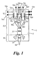
- the laser assembly 1 can be divided into essentially three sections: the DBR laser 10, the optical coupler 20, and the optical amplifier 30, all of which are integrally formed on a single substrate 2.
- the laser section 10 includes a plurality of individual DBR lasers 12a, 12b, 12c, 12d. Each DBR laser is individually activated, by injecting a current (I laser ) via electrical connections 13a, 13b, 13c and 13d respectively. Each DBR laser includes a grating 15a, 15b, 15c and 15d respectively, which is formed on the surfaces of the laser in a manor well know in the art. The tuning of each laser is achieved by injecting a further current (I grating ) to the gratings via further electrical connections 14a, 14b, 14c and 14d respectively. Thus it is possible to both individually activate each DBR laser and to tune each laser.
- the laser section 10 has two parts, an active section 10a and a tuning section 10b.
- the active section comprising of essentially a multiple quantum well layer 101 surrounded by an upper 104 and lower 105 cladding layers.
- a cap layer 107 is located on top of the upper cladding layer followed by metal contact layer 108.
- a high reflective coating 106 is deposited on the end face 102 of the laser section.
- the tuning section 10b consists of essentially a waveguide layer 110 surrounded by a an upper 112 and lower 111 cladding regions having lower refractive indices than the waveguide layer.
- a grating structure 15c is formed and surrounded by the upper cladding layer.
- a metal contact layer 118 is deposited on top of the upper cladding layer.
- the peak emission wavelength of each laser device By appropriately selecting the peak emission wavelength of each laser device, it is possible to create a laser source, which is capable of being tuned over a quasi-continuous range of wavelengths.
- the four DBR laser 12a, 12b, 12c, and 12d are chosen with peak emission wavelengths of 1523nm, 1533nm, 1543nm, and 1553nm respectively, and each laser is was capable of being tuned by + 12nm.
- the resulting laser source has an effective wavelength range covering over 40nm from 1523nm to 1565nm. This wavelength range more than covers the C band transmission spectrum, which is from 1530nm to 1560nm.
- the peak emission wavelength and tuneable range can be selected according to the wavelength range required for that particular laser source.
- the passive output end 17a, 17b, 17c, 17d of the individual DBR lasers is coupled to a waveguide 18a, 18b, 18c, 18d respectively.
- the waveguides are formed as an integral part of the substrate 2.
- Each waveguide is also coupled to an optical coupler 21.
- the optical coupler can be multimode interference (MMI) coupler, or alternatively, a Star coupler.
- MMI multimode interference
- SOA semiconductor optical amplifier
- section 20 consists of a waveguide layer 18c surrounded by an upper 212 and lower 211 cladding regions having lower refractive indices than the waveguide layer.
- the waveguide layer 18c may be the same material as the waveguide layer 110 in section 10b.
- the multimode interference coupler 21 is formed at the end of section 20 adjacent to section 30.
- the SOA is disposed in the third section 30 of the laser assembly and is integrally formed in substrate 2.
- the SOA comprises of essentially a multiple quantum well layer 301 surrounded by an upper 304 and lower 305 cladding layers.
- a cap layer 307 is located on top of the upper cladding layer followed by metal contact layer 308.
- An anti reflective coating 306 is deposited on the end face 302 of the SOA section.
- the SOA functions to recover, through amplification, all the optical losses that occur as the light propagated from the laser towards the output 60 of the laser source.
- figure 2b which is a cross section taken along the path labelled A-A in figure 2a, and in which features shown also appearing in figure 1 have the same reference numbers, all the components of the laser assembly are integrally formed on a single substrate 2. This is highly desirable from a manufacturing perspective and enables a compact, low cost tuneable laser source to be made.
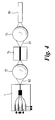
- FIG 4 a further embodiment of the present invention is shown in which the output 60 of laser assembly 1 described above is coupled via ball lens 72 to external modulator 75.
- the output 61 of the modulator is coupled via a second ball lens 73 to output optical fibre 80.
- the operation of the modulator is well known.
- the above embodiment demonstrates how the laser assembly of the present invention can be used in a modulated communications network.
Abstract
The present invention describes a tuneable laser assembly having a plurality of discrete
tunable DBR lasers disposed on a substrate and coupled to waveguides and an amplifier
via an optical coupler, all integrally formed on the substrate. The assembly can be
tuneable over a quasi-continuous range of wavelengths depending on the peak emission,
tuning range, and number of laser used.
Description
The present invention concerns a tuneable distributed Bragg reflector (DBR) laser
source, which is tuneable over a wide wavelength range and suitable for use in
wavelength division multiplexed (WDM) systems and fixed wavelength communication
systems.
More specifically, the present invention concerns a fully integrated tuneable laser
source in which the lasers device, optical coupler, and amplifier are all integrated on a
single substrate.
US patent number 5,394,489 discloses a tuneable laser source that comprises several
fixed wavelength distributed feedback (DFB) lasers disposed on a substrate. The lasers
are linked via waveguides to an optical coupler, such as the Star coupler, followed by an
amplifier and a modulator. Each laser is individually activated to emit a single
wavelength. Thus, depending on the emission wavelength of each laser, the device is
capable of emitting a series of discrete wavelengths.
Some tuning of the DFB laser may be possible by controlling the temperature of the
lasers, however this is costly and will not provide a laser source that is capable of
selectively emitting light covering a continuous range of wavelengths.
The present invention aims to produce a simple, low cost, fully integrated laser source
capable of being tuned over a wide range of continuous wavelengths.
Such a laser source has applications in WDM communications systems where several
wavelengths are multiplexed and transmitted down a single fibre.
Furthermore, such a tuneable laser source also has applications in single wavelength
communication systems, where it is desirable from a manufacturing point of view, to
stock a single laser source, which can be used in a variety of optical modules.
Depending on the customer's wavelength requirements, the tuneable laser source can be
fitted into the module and the appropriate wavelength selected. This has the advantage
of reducing inventory and enabling volume production of a single laser source for many
types of optical modules.
The object of the present invention is thus to provide a tunable laser source, which
overcomes the drawbacks of the solutions of the prior art considered above.
According to the present invention there is provided a tuneable laser assembly
comprising a substrate having formed thereon a plurality of tuneable DRB lasers, a
plurality of waveguides coupled to each of said lasers respectively, an optical coupler
coupled to said waveguides, and an amplifier coupled to said optical coupler, said lasers
having peak emission wavelengths and tuning ranges such that said laser assembly can
be tuned over a quasi-continuous predetermined wavelength range.
The waveguides, optical coupler, and amplifier may be all integrally formed on the
substrate.
While the principle features and advantages of the present invention have been
described above, a greater understanding and appreciation of the invention can be
obtained from the following figures and detailed description of the preferred
embodiment, in which;
As seen in figures 1, 2a and 2b, the laser assembly 1 can be divided into essentially
three sections: the DBR laser 10, the optical coupler 20, and the optical amplifier 30, all
of which are integrally formed on a single substrate 2.
The laser section 10 includes a plurality of individual DBR lasers 12a, 12b, 12c, 12d.
Each DBR laser is individually activated, by injecting a current (Ilaser) via electrical
connections 13a, 13b, 13c and 13d respectively. Each DBR laser includes a grating
15a, 15b, 15c and 15d respectively, which is formed on the surfaces of the laser in a
manor well know in the art. The tuning of each laser is achieved by injecting a further
current (Igrating) to the gratings via further electrical connections 14a, 14b, 14c and 14d
respectively. Thus it is possible to both individually activate each DBR laser and to
tune each laser.
The laser section 10 has two parts, an active section 10a and a tuning section 10b. The
active section comprising of essentially a multiple quantum well layer 101 surrounded
by an upper 104 and lower 105 cladding layers. A cap layer 107 is located on top of the
upper cladding layer followed by metal contact layer 108. A high reflective coating 106
is deposited on the end face 102 of the laser section.
The tuning section 10b consists of essentially a waveguide layer 110 surrounded by a an
upper 112 and lower 111 cladding regions having lower refractive indices than the
waveguide layer. A grating structure 15c is formed and surrounded by the upper
cladding layer. A metal contact layer 118 is deposited on top of the upper cladding
layer.
The operation and tuning of DBR lasers is well known in the art and thus will not be
described here in further detail.
By appropriately selecting the peak emission wavelength of each laser device, it is
possible to create a laser source, which is capable of being tuned over a quasi-continuous
range of wavelengths. For example, as seen in figure 3, the four DBR laser
12a, 12b, 12c, and 12d are chosen with peak emission wavelengths of 1523nm,
1533nm, 1543nm, and 1553nm respectively, and each laser is was capable of being
tuned by + 12nm. The resulting laser source has an effective wavelength range
covering over 40nm from 1523nm to 1565nm. This wavelength range more than covers
the C band transmission spectrum, which is from 1530nm to 1560nm.
In may be advantageous to select individual DRB lasers with a peak emission
wavelengths and tuning ranges so that there is a small overlap 33 with the peak
emission wavelength of the next laser.
As will be appreciated, the peak emission wavelength and tuneable range, as well as the
number of individual laser devices, can be selected according to the wavelength range
required for that particular laser source.
Now turning to section 20 of figure 1, the passive output end 17a, 17b, 17c, 17d of the
individual DBR lasers is coupled to a waveguide 18a, 18b, 18c, 18d respectively. The
waveguides are formed as an integral part of the substrate 2. Each waveguide is also
coupled to an optical coupler 21. The optical coupler can be multimode interference
(MMI) coupler, or alternatively, a Star coupler. The optical coupler functions to receive
light emitted by the activated laser device and transmitted via its corresponding
waveguide and transmit this light to semiconductor optical amplifier (SOA) 31.
As seen in figure 2b, section 20 consists of a waveguide layer 18c surrounded by an
upper 212 and lower 211 cladding regions having lower refractive indices than the
waveguide layer. The waveguide layer 18c may be the same material as the waveguide
layer 110 in section 10b. The multimode interference coupler 21 is formed at the end of
section 20 adjacent to section 30.
The SOA is disposed in the third section 30 of the laser assembly and is integrally
formed in substrate 2. The SOA comprises of essentially a multiple quantum well layer
301 surrounded by an upper 304 and lower 305 cladding layers. A cap layer 307 is
located on top of the upper cladding layer followed by metal contact layer 308. An anti
reflective coating 306 is deposited on the end face 302 of the SOA section.
The SOA functions to recover, through amplification, all the optical losses that occur as
the light propagated from the laser towards the output 60 of the laser source.
As can be clearly seen in figure 2b, which is a cross section taken along the path
labelled A-A in figure 2a, and in which features shown also appearing in figure 1 have
the same reference numbers, all the components of the laser assembly are integrally
formed on a single substrate 2. This is highly desirable from a manufacturing
perspective and enables a compact, low cost tuneable laser source to be made.
In figure 4 a further embodiment of the present invention is shown in which the output
60 of laser assembly 1 described above is coupled via ball lens 72 to external modulator
75. The output 61 of the modulator is coupled via a second ball lens 73 to output optical
fibre 80. The operation of the modulator is well known. The above embodiment
demonstrates how the laser assembly of the present invention can be used in a
modulated communications network.
It is not intended that the present invention be limited to the above embodiments and
other modifications and variations are envisaged within the scope of the claims.
Claims (11)
- A tuneable laser assembly comprising:said lasers having peak emission wavelengths and tuning ranges such that said laser assembly can be tuned over a quasi-continuous predetermined wavelength range.a substrate (2) having formed thereon a plurality of tuneable DRB lasers (12a, 12b, 12c, 12d),a plurality of waveguides (18a, 18b, 18c, 18d) coupled to each of said lasers respectively,an optical coupler (21) coupled to said waveguides, andan amplifier (31) coupled to said optical coupler,
- A laser assembly as claimed in Claim 1, wherein said lasers, waveguides, optical coupler, and amplifier are all integrally formed on said substrate.
- A laser assembly as claimed in Claim 2, wherein said amplifier has sufficient gain so to enable said assembly to output light of substantially the same intensity as output by any one of said lasers.
- A laser assembly as claimed in any preceding Claim, wherein said optical coupler is a multimode interference coupler.
- A laser assembly as claimed in any preceding claim, wherein said plurality of lasers have peak emission wavelengths and are sufficiently tunable so as to enable said assembly to emit any wavelength selected from said predetermined quasi-continuous wavelength range.
- A laser assembly as claimed in Claim 5, wherein said predetermined quasi-continuous wavelength range is covers the C transmission band.
- A laser assembly as claimed in Claims 5 or 6, wherein said predetermined quasi-continuous wavelength range is from approximately 1523nm to 1565nm.
- A laser assembly as claimed in any preceding Claim, wherein said assembly comprises four lasers.
- A laser assembly as claimed in Claim 8, wherein said four lasers (12a, 12b, 12c, 12d) have peak emission wavelengths at 1523nm, 1533nm, 1543nm and 1553nm respectively.
- A laser assembly as claimed in Claim 9, wherein said lasers can be tuned +12nm.
- A laser assembly as claimed in any preceding Claim, wherein said lasers are tuned by applying a current to a grating (15a, 15b, 15c, 15d) formed thereon.
Priority Applications (1)
| Application Number | Priority Date | Filing Date | Title |
|---|---|---|---|
| EP03251493A EP1458069A1 (en) | 2003-03-12 | 2003-03-12 | Widely tunable DBR laser source |
Applications Claiming Priority (1)
| Application Number | Priority Date | Filing Date | Title |
|---|---|---|---|
| EP03251493A EP1458069A1 (en) | 2003-03-12 | 2003-03-12 | Widely tunable DBR laser source |
Publications (1)
| Publication Number | Publication Date |
|---|---|
| EP1458069A1 true EP1458069A1 (en) | 2004-09-15 |
Family
ID=32748981
Family Applications (1)
| Application Number | Title | Priority Date | Filing Date |
|---|---|---|---|
| EP03251493A Withdrawn EP1458069A1 (en) | 2003-03-12 | 2003-03-12 | Widely tunable DBR laser source |
Country Status (1)
| Country | Link |
|---|---|
| EP (1) | EP1458069A1 (en) |
Cited By (1)
| Publication number | Priority date | Publication date | Assignee | Title |
|---|---|---|---|---|
| WO2006130094A1 (en) * | 2005-05-30 | 2006-12-07 | Phoxtal Communications Ab | Integrated chip |
Citations (2)
| Publication number | Priority date | Publication date | Assignee | Title |
|---|---|---|---|---|
| EP0606093A2 (en) * | 1993-01-07 | 1994-07-13 | Nec Corporation | Semiconductor optical integrated circuits and method for fabricating the same |
| US20010008539A1 (en) * | 1998-04-23 | 2001-07-19 | Nec Corporation | Method of manufacturing a semiconductor optical waveguide array and an array-structured semiconductor optical device |
-
2003
- 2003-03-12 EP EP03251493A patent/EP1458069A1/en not_active Withdrawn
Patent Citations (2)
| Publication number | Priority date | Publication date | Assignee | Title |
|---|---|---|---|---|
| EP0606093A2 (en) * | 1993-01-07 | 1994-07-13 | Nec Corporation | Semiconductor optical integrated circuits and method for fabricating the same |
| US20010008539A1 (en) * | 1998-04-23 | 2001-07-19 | Nec Corporation | Method of manufacturing a semiconductor optical waveguide array and an array-structured semiconductor optical device |
Non-Patent Citations (1)
| Title |
|---|
| KOREN U ET AL: "WAVELENGTH DIVISION MULITPLEXING LIGHT SOURCE WITH INTEGRATED QUANTUM WELL TUNABLE LASERS AND OPTICAL AMPLIFIERS", APPLIED PHYSICS LETTERS, AMERICAN INSTITUTE OF PHYSICS. NEW YORK, US, vol. 54, no. 21, 22 May 1989 (1989-05-22), pages 2056 - 2058, XP000080585, ISSN: 0003-6951 * |
Cited By (2)
| Publication number | Priority date | Publication date | Assignee | Title |
|---|---|---|---|---|
| WO2006130094A1 (en) * | 2005-05-30 | 2006-12-07 | Phoxtal Communications Ab | Integrated chip |
| US7599586B2 (en) | 2005-05-30 | 2009-10-06 | Phoxtal Communications Ab | Integrated chip |
Similar Documents
| Publication | Publication Date | Title |
|---|---|---|
| US7424041B2 (en) | Wide tuneable laser sources | |
| EP0930679B1 (en) | Wavelength selectable laser source for wavelength division multiplexed applications | |
| US8295315B2 (en) | Tunable laser | |
| US6628686B1 (en) | Integrated multi-wavelength and wideband lasers | |
| US7277462B2 (en) | Wide tuneable laser sources | |
| US8643943B2 (en) | Tunable laser source using intracavity laser light outcoupling and module containing the same | |
| KR100547897B1 (en) | Tunable Laser Device | |
| US7194157B2 (en) | Method and apparatus providing an output coupler for an optical beam | |
| US20110292960A1 (en) | Wavelength tunable semiconductor laser | |
| US8548024B2 (en) | Semiconductor laser module | |
| US9013785B2 (en) | Tunable multi-mode laser | |
| KR100420950B1 (en) | Tunable wavelength laser light source | |
| KR101003053B1 (en) | a wavelength-tunable external cavity laser | |
| JP2013118315A (en) | Semiconductor laser device and semiconductor laser module | |
| US20090268762A1 (en) | Optical intergrated device | |
| Den Besten et al. | An integrated 4 x 4-channel multiwavelength laser on InP | |
| EP1458069A1 (en) | Widely tunable DBR laser source | |
| US6567446B1 (en) | Optical device with increased spectral width | |
| JP2006203100A (en) | Semiconductor laser and light transmitter module | |
| US6363093B1 (en) | Method and apparatus for a single-frequency laser | |
| Gotoda et al. | Dual-output tunable laser diode array for optical transmission and coherent detection | |
| JP2012156414A (en) | Semiconductor laser element and semiconductor laser device | |
| EP2169788A1 (en) | Wavelength selective element, process for adjusting the refraction index of a wavelength selective element, and optical radiation emitting component | |
| JP2009088192A (en) | Semiconductor laser | |
| JP3600785B2 (en) | Waveguide type laser |
Legal Events
| Date | Code | Title | Description |
|---|---|---|---|
| PUAI | Public reference made under article 153(3) epc to a published international application that has entered the european phase |
Free format text: ORIGINAL CODE: 0009012 |
|
| AK | Designated contracting states |
Kind code of ref document: A1 Designated state(s): AT BE BG CH CY CZ DE DK EE ES FI FR GB GR HU IE IT LI LU MC NL PT RO SE SI SK TR |
|
| AX | Request for extension of the european patent |
Extension state: AL LT LV MK |
|
| AKX | Designation fees paid | ||
| REG | Reference to a national code |
Ref country code: DE Ref legal event code: 8566 |
|
| STAA | Information on the status of an ep patent application or granted ep patent |
Free format text: STATUS: THE APPLICATION IS DEEMED TO BE WITHDRAWN |
|
| 18D | Application deemed to be withdrawn |
Effective date: 20050316 |