EP1458027A1 - Semiconductor device - Google Patents
Semiconductor device Download PDFInfo
- Publication number
- EP1458027A1 EP1458027A1 EP02781808A EP02781808A EP1458027A1 EP 1458027 A1 EP1458027 A1 EP 1458027A1 EP 02781808 A EP02781808 A EP 02781808A EP 02781808 A EP02781808 A EP 02781808A EP 1458027 A1 EP1458027 A1 EP 1458027A1
- Authority
- EP
- European Patent Office
- Prior art keywords
- wiring
- shield
- wirings
- layer
- wiring layer
- Prior art date
- Legal status (The legal status is an assumption and is not a legal conclusion. Google has not performed a legal analysis and makes no representation as to the accuracy of the status listed.)
- Withdrawn
Links
Images





Classifications
-
- H—ELECTRICITY
- H10—SEMICONDUCTOR DEVICES; ELECTRIC SOLID-STATE DEVICES NOT OTHERWISE PROVIDED FOR
- H10W—GENERIC PACKAGES, INTERCONNECTIONS, CONNECTORS OR OTHER CONSTRUCTIONAL DETAILS OF DEVICES COVERED BY CLASS H10
- H10W20/00—Interconnections in chips, wafers or substrates
- H10W20/40—Interconnections external to wafers or substrates, e.g. back-end-of-line [BEOL] metallisations or vias connecting to gate electrodes
- H10W20/495—Capacitive arrangements or effects of, or between wiring layers
-
- H—ELECTRICITY
- H10—SEMICONDUCTOR DEVICES; ELECTRIC SOLID-STATE DEVICES NOT OTHERWISE PROVIDED FOR
- H10W—GENERIC PACKAGES, INTERCONNECTIONS, CONNECTORS OR OTHER CONSTRUCTIONAL DETAILS OF DEVICES COVERED BY CLASS H10
- H10W20/00—Interconnections in chips, wafers or substrates
- H10W20/40—Interconnections external to wafers or substrates, e.g. back-end-of-line [BEOL] metallisations or vias connecting to gate electrodes
- H10W20/41—Interconnections external to wafers or substrates, e.g. back-end-of-line [BEOL] metallisations or vias connecting to gate electrodes characterised by their conductive parts
- H10W20/423—Shielding layers
Definitions
- the present invention relates to a wiring structure of a semiconductor device.
- FIG. 28 shows an example of wiring only using a single wiring layer.
- the wiring layer has a tight arrangement. In this way, as a wiring layer making contact with the source or drain of a device such as a transistor, the lowest wiring layer is generally used, and the minimum wiring is frequently provided according to a pitch of contact.
- the conventional semiconductor device increases a capacitance between adjacent wirings and increases noise between adjacent wirings, lowering the operating speed of signals.
- an object of the present invention is to provide a semiconductor device which can reduce a capacitance between adj acent wirings, noise between adjacent wirings, and power consumption without lowering the operating speed of a signal.
- a semiconductor device according to the present invention has the following wiring structure.
- Wirings are formed in a plurality of wiring layers and a distance is increased between the wiring layers to reduce noise between the wiring layers. First, a capacitance between wirings between the layers is reduced, and wirings in a first wiring layer and a second wiring layer are arranged on different positions taken from the top, so that a capacitance between wirings can be reducedbetween the first wiring layer and second wiring layer.
- a first wiring, a first shield wiring, and a second wiring are arranged in this order in the first wiring layer, and a third wiring, a second shield wiring, and a fourth wiring are arranged in this order in the second wiring layer.
- the first shield wiring and the second shield wiring are ground voltage lines or power voltage lines. Further, the ground voltage lines and the power voltage lines are alternately arranged, or the first wiring layer is used as a ground voltage line and the second wiring layer is used as a power voltage line.
- the arrangement has two wiring layer regions and the wirings of the wiring layer regions are connected to each other, so that the wiring structure can offer a preferred balance of a resistance and a capacitance.
- the shield wiring is larger in width than the signal wiring in the wiring structure.
- the lowest wiring layer is constituted of a single wiring layer as with the conventional art.
- An upper layer thereon has a wiring structure of a first wiring, a first shield wiring, and a second wiring that are arranged in this order.
- An upper layer thereon has a wiring structure of a third wiring, a second shield wiring, and a fourth wiring that are arranged in this order.
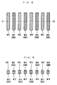
- FIG. 1 is a top view of Embodiment 1
- FIG. 2 is a sectional view taken along line A1-A2 of FIG. 1.
- wirings M12, M14, M16, and M18 are arranged in this order in a first wiring layer.
- signal lines M21, M23, M25, and M27 are arranged in this order in a second wiring layer.
- the signal lines in the first wiring layer and the second wiring layer are arranged at almost equal intervals.
- the signal lines M21 and M12, the signal lines M23 and M14, the signal lines M25 and M16, and the signal lines M27 and M18 are connected to amplifiers.
- the signal lines M12, M14, M16, and M18 and the signal lines M21, M23, M25, and M27 are arranged on different positions taken from the top. As compared with the case where the signal lines are arranged on the same positions taken from the top, noise can be reduced between the signal lines.
- Embodiment 1 has the following effect: the signal lines are arranged using the two wiring layers and shield wirings are placed between the signal lines, so that it is possible to reduce a capacitance between adjacent wirings, noise between adjacent wirings, and power consumption without reducing the operating speed of a signal. Particularly, since the signal lines of the first wiring layer and the second wiring layer are arranged on different positions taken from the top, a great effect can be achieved.
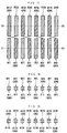
- FIG. 3 is a top view of Embodiment 2
- FIG. 4 is a sectional view taken along line A1-A2 of FIG. 3.
- a first wiring layer and a second wiring layer have adjacent signal lines in pairs in the present embodiment. Wirings are not arranged at equal intervals in each of the wiring layers. Further, the signals of the adjacent wirings are connected to amplifiers.
- Embodiment 2 has the following effect: signal lines are arranged using two wiring layers as with Embodiment 1, so that it is possible to reduce a capacitance between adjacent wirings, noise between adjacent wirings, and power consumption without reducing the operating speed of a signal. Particularly since the signal lines of the first wiring layer the second wiring layer are arranged on different positions taken from the top, a great effect can be achieved.
- the wirings connected to the same amplifier are arranged in the same layer, it is possible to reduce the influence of variations or the like during the manufacturing of the wirings.
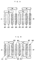
- FIG. 5 is a top view of Embodiment 3.
- electrically connected wirings are transferred to and from a first wiring layer and a second wiring layer at some midpoint in the present embodiment. Since this structure has both regions of the first wiring layer and the second wiring layer, the same arrangement is provided over the wirings.
- connection configuration of amplifiers is the same as Embodiment 1.
- FIG. 6 is a top view of Embodiment 4.
- electrically connected wirings are transferred to and from a first wiring layer and a second wiring layer at some midpoint in the present embodiment. Since this structure has both regions of the first wiring layer and the second wiring layer, so that the same arrangement is provided over the wirings.
- the electrically connected wirings on signals are not arranged almost like a straight line taken from the top but the wirings in the same wiring layer are arranged almost like a straight line.
- the configuration of connecting the amplifiers is the same as that of Embodiment 1.
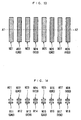
- FIG. 7 is a top view of Embodiment 5.
- the wiring constitution is the same as Embodiment 3 but the connecting positions of amplifiers are different from those of Embodiment 3. Two wirings connected to the same amplifier are arranged on the same position in the wiring direction in the same wiring layer.
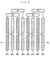
- FIG. 8 is a top view of Embodiment 6.
- Embodiment 4 and Embodiment 5 are combined in the present embodiment and the same effects of the embodiments 4 and 5 are obtained.
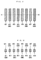
- FIG. 9 is a top view of Embodiment 7.
- the arrangement of connected amplifiers is changed from the wiring constitution of Embodiment 2.
- a signal wiring connected to the amplifier not being operated has the effect of a shield wiring.
- the same effect can be obtained as the case where a shield wiring is arranged on an adjacent wiring in the same layer.
- FIG. 10 is a top view of Embodiment 8.
- the arrangement of connected amplifiers is changed and the amplifiers are placed on both ends of a wiring.
- this arrangement like Embodiment 5, two wirings connected to the same amplifier are arranged on the same position in the wiring direction in the same wiring layer. When a signal wiring crosses two wirings connected to the same amplifier, noise from the signal can be cancelled.
- FIG. 11 is a top view of Embodiment 9, and FIG. 12 is a sectional view taken along line A1-A2 of FIG. 11. Only the wiring of a second wiring layer on the upper surface side is illustrated in the top view.
- wirings M11 to M18 are arranged in this order in a first wiring layer.
- the wirings M12, M14, M16, and M18 are used as signal lines.
- the wirings M11, M13, M15, and M17 arranged between the signal lines M12, M14, M16, and M18 are provided as shield wirings for reducing noise on the signal lines.
- wirings M21 to M28 are arranged in this order in the second wiring layer.
- the wirings M21, M23, M25, and M27 are used as signal lines.
- the wirings M22, M24, M26, and M28 arranged between the signal lines M21, M23, M25, and M27 are provided as shield wirings for reducing the noise of the signal lines.
- the signal lines M12, M14, M16, and M18 and the signal lines M21, M23, M25, and M27 are arranged on different positions taken from the top, and the shield wirings are arranged between the signal lines.
- the shielding effect between the signal lines can be increased as compared with the case where the signal lines are arranged on the same positions taken from the top, thereby further reducing the noise of the signal lines.
- the shield wirings are connected to a ground voltage line (GND potential) in this arrangement, the shield wirings may be connected to a power voltage line.
- Embodiment 9 has the following effect: the signal lines are arranged using the two wiring layers and the shield wirings are arranged between the signal lines, so that it is possible to reduce a capacitance between adjacent wirings, noise between adjacent wirings, and power consumption without reducing the operating speed of a signal. Particularly since the signal lines of the first wiring layer and the second wiring layer are arranged on different positions taken from the top, achieving a great effect of shielding noise.
- ground voltage line serving as a shield wiring may be used as a ground voltage line wired from a power supply or the like.
- FIG. 13 is a top view of Embodiment 10
- FIG. 14 is a sectional view taken along line A1-A2 of FIG. 13. Only the wiring of a second wiring layer on the upper surface side is illustrated in the top view.
- Embodiment 10 is characterized in that shield wirings are connected to both of a ground voltage line and a power voltage line.
- Shield wirings M11, M13, M15, and M17 in a first wiring layer are connected alternately to the ground voltage line and the power voltage line
- shield wirings M22, M24, M26, and M28 in a second wiring layer are connected alternately to the ground voltage line and the power voltage line.
- the shield wirings are connected alternately to the ground voltage line and the power voltage line, the order is not always limited and the most suitable setting can be used in accordance with the layout.
- Embodiment 10 has the same effect as Embodiment 9, and the shield wirings on both of the ground voltage line and the power voltage line are used. Thus, the signals can be used as power supply signals of the circuit.
- FIG. 15 is a top view of Embodiment 11, and FIG. 16 is a sectional view taken along line A1-A2 of FIG. 15. Only the wiring of a second wiring layer on the top surface side is illustrated in the top view.
- Embodiment 11 is characterized in that shield wirings in a first wiring layer are connected to a power voltage line and shield wirings in the second wiring layer are connected to a ground voltage line.
- shield wirings M11, M13, M15, and M17 in a first wiring layer are connected to the power voltage line (VDD potential) and shield wirings M22, M24, M26, and M28 in a second wiring layer are connected to the ground voltage line (GND potential).
- the shield wirings in the first wiring layer are used as the power voltage line and the shield wirings in the second wiring layer are used as the ground voltage line.
- the reversed arrangement can be used as necessary.
- the shield wirings in the same wiring layer are used as the same voltage line, achieving a simple layout.
- Embodiment 11 has the same effect as Embodiment 9 and Embodiment 10.
- the shield wirings in the same wiring layer are used as the same voltage line, achieving a simple layout.
- FIG. 17 is a top view of Embodiment 12
- FIG. 18 is a sectional view taken along line A1-A2 of FIG. 17,
- FIG. 19 is a sectional view taken along line B1-B2 of FIG. 17. Only the wiring of a second wiring layer on the top surface side is illustrated in the top view.
- a wiring region is broadly divided into two regions and the two regions of the wiring constitutions in Embodiment 9 are provided. Further, the wiring of a first wiring layer and the wiring of the second wiring layer in the two regions are replaced with each other and are connected to each other. With this arrangement, each of the wirings is provided both in the first wiring layer and the second wiring layer, so that a balance of a capacitance and a resistance can be offered on the wirings and a stable operation can be performed when the wirings are used as bit lines or the like of a memory.
- wirings M11 to M18 are arranged in this order in the first wiring layer.
- wirings M12, M14, M16, and M18 are used as signal lines.
- the wirings M11, M13, M15, and M17 arranged between the signal lines M12, M14, M16, and M18 are used as shield wirings for reducing the noise of the signal lines.
- wirings M21 to M28 are arranged in this order in the second wiring layer.
- the wirings M21, M23, M25, and M27 are used as signal lines.
- the wirings M22, M24, M26, and M28 arranged between the signal lines M21, M23, M25, and M27 are used as shield wirings for reducing the noise of the signal lines.
- the line M12 is connected to a line M22B
- the line M14 is connected to a line M24B
- the line M16 is connected to a line M26B
- the line M18 is connected to M28B
- the line M21 is connected to a line M11B
- the line M23 is connected to a line M13B
- the line M25 is connected to a line M15B
- the line M27 is connected to a line M17B.
- the shield wirings are connected to a ground voltage line (GND potential).
- the shield wirings may be connected to a power voltage line, or both of the ground voltage line and the power voltage line may be used.
- the arrangement is constituted of the two wiring regions, more wiring regions may be provided. When the number of wiring regions is increased, it is possible to offer a preferred balance of a capacitance and a resistance on each of the wirings.
- Embodiment 12 has the same effect as -Embodiment 9.
- the wiring region is divided into two or more regions and the wirings of the regions are replaced with each other before being connected, so that a balance of a capacitance and a resistance on each of the wirings is improved and a stable operation can be performed.
- FIG. 20 is a top view of Embodiment 13
- FIG. 21 is a sectional view taken along line A1-A2 of FIG. 20. Only the wiring of a second wiring layer on the top surface side is illustrated in the top view.
- Embodiment 13 is characterized in that a shield wiring is larger in width than a signal line.
- Shield wirings M11, M13, M15, and M17 in a first wiring layer and shield wirings M22, M24, M26, and M28 in a second wiring layer are larger in width than signal lines M12, M14, M16, M18, M21, M23, M25, and M27.
- Embodiment 13 has the same effect as Embodiment 9. With a larger width of the shield wiring, the shielding effect can be higher than that of Embodiment 9.
- the shield wirings in the first wiring layer and the shield wirings in the second wiring layer do not overlap each other in the present embodiment.
- the shielding effect can be further increased.
- FIG. 22 is a top view of Embodiment 14
- FIG. 23 is a sectional view taken along line A1-A2 of FIG. 22. Only the wiring of a second wiring layer on the top surface side is illustrated in the top view.
- a shield layer M31 serving as a third wiring layer is placed between the first wiring layer and the second wiring layer.
- Embodiment 14 Since Embodiment 14 has the shield layer M31 placed as the third wiring layer, the shielding effect can be increased.
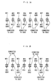
- FIG. 24 is a diagram showing a connecting relationship with sense amplifiers.
- Signal lines M12 and M21, signal lines M14 and M23, signal lines M16 and M25, and signal lines M18 and M27 are connected to sense amplifiers SA01, SA02, SA03, and SA04, respectively.
- adjacent signal lines of the signal lines in a first wiring layer and a second wiring layer are connected to the sense amplifiers.
- this arrangement is used for bit lines of a memory, adjacent memory cells can be used and thus a stable operation can be obtained for the memory.
- FIG. 25 shows a connecting relationship with sense amplifiers.
- Signal lines M21 and M23, signal lines M12 and M14, signal lines M25 and M27, and signal lines M16 and M18 are connected to sense amplifiers SA01, SA02, SA03, and SA04, respectively.
- the signal lines connected to the sense amplifier can be separated away from each other, thereby reducing the influence of noise between adjacent signal lines.
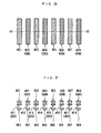
- FIG. 26 is a top view of Embodiment 17, and FIG. 27 is a sectional view taken along line A1-A2 of FIG. 26. Only the wiring of a second wiring layer on the top surface side is illustrated in the top view.
- Signal lines are arranged by combining the arrangement of Embodiment 9 and a conventional arrangement which is tightly wired as the lowest wiring layer.
- the wiring of the lowest layer and the signal lines of a first wiring layer and a second wiring layer are electrically connected to each other.
- This arrangement is used for a memory array using a main bit line and a sub bit line, so that it is possible to achieve a memory array capable of reducing a capacitance between adjacent wirings and noise between adjacent wirings without lowering the operating speed of a signal.
- Embodiment 7 is also applicable to the other embodiments.
- signal lines connected to amplifiers are used as shield wirings, thereby reducing noise.
- Embodiment 17 described that the wirings in the lowest layer are arranged in the conventional structure. This arrangement is also applicable to the other embodiments.
Landscapes
- Semiconductor Integrated Circuits (AREA)
- Design And Manufacture Of Integrated Circuits (AREA)
- Internal Circuitry In Semiconductor Integrated Circuit Devices (AREA)
Abstract
A first wiring layer overlying a semiconductor substrate
has the arrangement of adjacent wirings in the order of first
wirings and first shield wirings. A second wiring layer
overlying the semiconductor substrate has the arrangement of
adjacent wirings in the order of second shield wirings and
second wirings to correspond to the respective first wirings
and first shield wirings in the first wiring layer. Thus,
the capacitance between adjacent wirings is reduced as well
as the noise between adjacent wirings. Further, power
consumption is reduced without a decrease in the action speed
of a signal.
Description
The present invention relates to a wiring structure of
a semiconductor device.
As the designs of semiconductor devices become finer,
a capacitance between wirings has become a problem on circuit
designs. Particularly, a capacitance between adjacent
wirings delays the driving time of signal lines.
Referring to FIG. 28, an example of a conventional wiring
structure will be briefly described. FIG. 28 shows an example
of wiring only using a single wiring layer. The wiring layer
has a tight arrangement. In this way, as a wiring layer making
contact with the source or drain of a device such as a transistor,
the lowest wiring layer is generally used, and the minimum
wiring is frequently provided according to a pitch of contact.
However, the conventional semiconductor device increases
a capacitance between adjacent wirings and increases noise
between adjacent wirings, lowering the operating speed of
signals.
Further, as a capacitance between wirings becomes larger,
power consumption also increases.
Moreover, when the wiring structure is used for a bit
line of a memory, it is difficult to read a necessary potential
from a memory cell to the bit line.
Additionally, in reverse, in the case of memory such as
a ferroelectric memory or the like requiring a suitable wiring
capacitance, it is difficult to reduce noise between adjacent
wirings and set a suitable wiring capacitance at the same time.
Under the circumstances, an object of the present
invention is to provide a semiconductor device which can reduce
a capacitance between adj acent wirings, noise between adjacent
wirings, and power consumption without lowering the operating
speed of a signal.
A semiconductor device according to the present invention
has the following wiring structure.
Wirings are formed in a plurality of wiring layers and
a distance is increased between the wiring layers to reduce
noise between the wiring layers. First, a capacitance between
wirings between the layers is reduced, and wirings in a first
wiring layer and a second wiring layer are arranged on different
positions taken from the top, so that a capacitance between
wirings can be reducedbetween the first wiring layer and second
wiring layer.
Moreover, the following wiring structure is provided:
a first wiring, a first shield wiring, and a second wiring
are arranged in this order in the first wiring layer, and a
third wiring, a second shield wiring, and a fourth wiring are
arranged in this order in the second wiring layer.
Besides, the first shield wiring and the second shield
wiring are ground voltage lines or power voltage lines.
Further, the ground voltage lines and the power voltage lines
are alternately arranged, or the first wiring layer is used
as a ground voltage line and the second wiring layer is used
as a power voltage line.
Moreover, the arrangement has two wiring layer regions
and the wirings of the wiring layer regions are connected to
each other, so that the wiring structure can offer a preferred
balance of a resistance and a capacitance.
Moreover, the shield wiring is larger in width than the
signal wiring in the wiring structure.
Besides, the lowest wiring layer is constituted of a single
wiring layer as with the conventional art. An upper layer
thereon has a wiring structure of a first wiring, a first shield
wiring, and a second wiring that are arranged in this order.
An upper layer thereon has a wiring structure of a third wiring,
a second shield wiring, and a fourth wiring that are arranged
in this order.
According to these arrangements of the semiconductor
device, it is possible to reduce a capacitance between adj acent
wirings, noise between adjacent wirings, andpower consumption
without lowering the operating speed of a signal.
With reference to the accompanying drawings, a
semiconductor device according to embodiments of the present
invention will be specifically described below.
Embodiment 1 of the present invention will be discussed
below according to the accompanying drawings. FIG. 1 is a
top view of Embodiment 1, and FIG. 2 is a sectional view taken
along line A1-A2 of FIG. 1.
First, wirings (e.g., signal lines) M12, M14, M16, and
M18 are arranged in this order in a first wiring layer. Then,
on the first wiring layer, signal lines M21, M23, M25, and
M27 are arranged in this order in a second wiring layer. In
this case, the signal lines in the first wiring layer and the
second wiring layer are arranged at almost equal intervals.
Further, the signal lines M21 and M12, the signal lines M23
and M14, the signal lines M25 and M16, and the signal lines
M27 and M18 are connected to amplifiers. In the present
embodiment, the signal lines M12, M14, M16, and M18 and the
signal lines M21, M23, M25, and M27 are arranged on different
positions taken from the top. As compared with the case where
the signal lines are arranged on the same positions taken from
the top, noise can be reduced between the signal lines.
Embodiment 1 has the following effect: the signal lines
are arranged using the two wiring layers and shield wirings
are placed between the signal lines, so that it is possible
to reduce a capacitance between adjacent wirings, noise
between adjacent wirings, and power consumption without
reducing the operating speed of a signal. Particularly, since
the signal lines of the first wiring layer and the second wiring
layer are arranged on different positions taken from the top,
a great effect can be achieved.
Embodiment 2 of the present invention will be discussed
below according to the accompanying drawings. FIG. 3 is a
top view of Embodiment 2, and FIG. 4 is a sectional view taken
along line A1-A2 of FIG. 3.
Unlike Embodiment 1, a first wiring layer and a second
wiring layer have adjacent signal lines in pairs in the present
embodiment. Wirings are not arranged at equal intervals in
each of the wiring layers. Further, the signals of the
adjacent wirings are connected to amplifiers.
Embodiment 2 has the following effect: signal lines are
arranged using two wiring layers as with Embodiment 1, so that
it is possible to reduce a capacitance between adjacent wirings,
noise between adjacent wirings, and power consumption without
reducing the operating speed of a signal. Particularly since
the signal lines of the first wiring layer the second wiring
layer are arranged on different positions taken from the top,
a great effect can be achieved.
Additionally, since the wirings connected to the same
amplifier are arranged in the same layer, it is possible to
reduce the influence of variations or the like during the
manufacturing of the wirings.
Embodiment 3 of the present invention will be discussed
below according to the accompanying drawings. FIG. 5 is a
top view of Embodiment 3.
Unlike Embodiment 1, electrically connected wirings are
transferred to and from a first wiring layer and a second wiring
layer at some midpoint in the present embodiment. Since this
structure has both regions of the first wiring layer and the
second wiring layer, the same arrangement is provided over
the wirings.
With this arrangement, it is possible to reduce the
influence of variations or the like during the manufacturing
of the wiring.
Further, the electrically connected wirings on signals
are arranged almost like a straight line taken from the top.
The connecting part of the wirings in the first wiring layer
and the second wiring layer do not intersect the other wirings,
achieving a simple layout. The connection configuration of
amplifiers is the same as Embodiment 1.
Embodiment 4 of the present invention will be discussed
below according to the accompanying drawings. FIG. 6 is a
top view of Embodiment 4.
Unlike Embodiment 1, electrically connected wirings are
transferred to and from a first wiring layer and a second wiring
layer at some midpoint in the present embodiment. Since this
structure has both regions of the first wiring layer and the
second wiring layer, so that the same arrangement is provided
over the wirings.
With this arrangement, it is possible to reduce the
influence of variations or the like during the manufacturing
of the wirings.
Further, taken from the top, the electrically connected
wirings on signals are not arranged almost like a straight
line taken from the top but the wirings in the same wiring
layer are arranged almost like a straight line. For example,
when another wiring layer is provided on the second wiring
in the same direction, almost equal noise is set for a pair
of wirings connected to the same amplifier, thereby reducing
the influence of noise. The configuration of connecting the
amplifiers is the same as that of Embodiment 1.
Embodiment 5 of the present invention will be discussed
below according to the accompanying drawings. FIG. 7 is a
top view of Embodiment 5.
In the present embodiment, the wiring constitution is
the same as Embodiment 3 but the connecting positions of
amplifiers are different from those of Embodiment 3. Two
wirings connected to the same amplifier are arranged on the
same position in the wiring direction in the same wiring layer.
With this arrangement, for example, when a signal wiring
crosses two wirings connected to the same amplifier, noise
from the signal can be cancelled.
Embodiment 6 of the present invention will be discussed
below according to the accompanying drawings. FIG. 8 is a
top view of Embodiment 6.
Embodiment 4 and Embodiment 5 are combined in the present
embodiment and the same effects of the embodiments 4 and 5
are obtained.
Embodiment 7 of the present invention will be discussed
below according to the accompanying drawings. FIG. 9 is a
top view of Embodiment 7.
In the present embodiment, the arrangement of connected
amplifiers is changed from the wiring constitution of
Embodiment 2. In this arrangement, for example, when a method
of operating one of two amplifiers is used, a signal wiring
connected to the amplifier not being operated has the effect
of a shield wiring. Hence, the same effect can be obtained
as the case where a shield wiring is arranged on an adjacent
wiring in the same layer.
Embodiment 8 of the present invention will be discussed
below according to the accompanying drawings. FIG. 10 is a
top view of Embodiment 8.
Unlike the wiring constitution of Embodiment 1, in the
present embodiment, the arrangement of connected amplifiers
is changed and the amplifiers are placed on both ends of a
wiring. In this arrangement, like Embodiment 5, two wirings
connected to the same amplifier are arranged on the same
position in the wiring direction in the same wiring layer.
When a signal wiring crosses two wirings connected to the same
amplifier, noise from the signal can be cancelled.
Embodiment 9 of the present invention will be discussed
below according to the accompanying drawings. FIG. 11 is a
top view of Embodiment 9, and FIG. 12 is a sectional view taken
along line A1-A2 of FIG. 11. Only the wiring of a second wiring
layer on the upper surface side is illustrated in the top view.
First, wirings M11 to M18 are arranged in this order in
a first wiring layer. The wirings M12, M14, M16, and M18 are
used as signal lines. The wirings M11, M13, M15, and M17
arranged between the signal lines M12, M14, M16, and M18 are
provided as shield wirings for reducing noise on the signal
lines.
Subsequently, on the first wiring layer, wirings M21 to
M28 are arranged in this order in the second wiring layer.
Here, the wirings M21, M23, M25, and M27 are used as signal
lines. The wirings M22, M24, M26, and M28 arranged between
the signal lines M21, M23, M25, and M27 are provided as shield
wirings for reducing the noise of the signal lines.
In the present embodiment, the signal lines M12, M14,
M16, and M18 and the signal lines M21, M23, M25, and M27 are
arranged on different positions taken from the top, and the
shield wirings are arranged between the signal lines. The
shielding effect between the signal lines can be increased
as compared with the case where the signal lines are arranged
on the same positions taken from the top, thereby further
reducing the noise of the signal lines. Further, although
the shield wirings are connected to a ground voltage line (GND
potential) in this arrangement, the shield wirings may be
connected to a power voltage line.
Embodiment 9 has the following effect: the signal lines
are arranged using the two wiring layers and the shield wirings
are arranged between the signal lines, so that it is possible
to reduce a capacitance between adjacent wirings, noise
between adjacent wirings, and power consumption without
reducing the operating speed of a signal. Particularly since
the signal lines of the first wiring layer and the second wiring
layer are arranged on different positions taken from the top,
achieving a great effect of shielding noise.
Further, the ground voltage line serving as a shield wiring
may be used as a ground voltage line wired from a power supply
or the like.
Embodiment 10 of the present invention will be discussed
below according to the accompanying drawings. FIG. 13 is a
top view of Embodiment 10, and FIG. 14 is a sectional view
taken along line A1-A2 of FIG. 13. Only the wiring of a second
wiring layer on the upper surface side is illustrated in the
top view.
The arrangement of signal lines is the same as Embodiment
9. Embodiment 10 is characterized in that shield wirings are
connected to both of a ground voltage line and a power voltage
line.
Shield wirings M11, M13, M15, and M17 in a first wiring
layer are connected alternately to the ground voltage line
and the power voltage line, and shield wirings M22, M24, M26,
and M28 in a second wiring layer are connected alternately
to the ground voltage line and the power voltage line.
Although the shield wirings are connected alternately to the
ground voltage line and the power voltage line, the order is
not always limited and the most suitable setting can be used
in accordance with the layout.
Embodiment 10 has the same effect as Embodiment 9, and
the shield wirings on both of the ground voltage line and the
power voltage line are used. Thus, the signals can be used
as power supply signals of the circuit.
Embodiment 11 of the present invention will be discussed
below according to the accompanying drawings. FIG. 15 is a
top view of Embodiment 11, and FIG. 16 is a sectional view
taken along line A1-A2 of FIG. 15. Only the wiring of a second
wiring layer on the top surface side is illustrated in the
top view.
The arrangement of signal lines is the same as Embodiment
9 and Embodiment 10. Embodiment 11 is characterized in that
shield wirings in a first wiring layer are connected to a power
voltage line and shield wirings in the second wiring layer
are connected to a ground voltage line.
To be specific, shield wirings M11, M13, M15, and M17
in a first wiring layer are connected to the power voltage
line (VDD potential) and shield wirings M22, M24, M26, and
M28 in a second wiring layer are connected to the ground voltage
line (GND potential).
In this case, the shield wirings in the first wiring layer
are used as the power voltage line and the shield wirings in
the second wiring layer are used as the ground voltage line.
The reversed arrangement can be used as necessary. The shield
wirings in the same wiring layer are used as the same voltage
line, achieving a simple layout.
Embodiment 11 has the same effect as Embodiment 9 and
Embodiment 10. Regarding the ground voltage line and the power
voltage line, the shield wirings in the same wiring layer are
used as the same voltage line, achieving a simple layout.
Embodiment 12 of the present invention will be discussed
below according to the accompanying drawings. FIG. 17 is a
top view of Embodiment 12, FIG. 18 is a sectional view taken
along line A1-A2 of FIG. 17, and FIG. 19 is a sectional view
taken along line B1-B2 of FIG. 17. Only the wiring of a second
wiring layer on the top surface side is illustrated in the
top view.
In Embodiment 12, a wiring region is broadly divided into
two regions and the two regions of the wiring constitutions
in Embodiment 9 are provided. Further, the wiring of a first
wiring layer and the wiring of the second wiring layer in the
two regions are replaced with each other and are connected
to each other. With this arrangement, each of the wirings
is provided both in the first wiring layer and the second wiring
layer, so that a balance of a capacitance and a resistance
can be offered on the wirings and a stable operation can be
performed when the wirings are used as bit lines or the like
of a memory.
The detailed arrangement will be discussed below. First,
in a first wiring region (cross section along line A1-A2 of
FIG. 18), wirings M11 to M18 are arranged in this order in
the first wiring layer. In this arrangement, wirings M12,
M14, M16, and M18 are used as signal lines. The wirings M11,
M13, M15, and M17 arranged between the signal lines M12, M14,
M16, and M18 are used as shield wirings for reducing the noise
of the signal lines.
Then, on the first wiring layer, wirings M21 to M28 are
arranged in this order in the second wiring layer. In this
arrangement, the wirings M21, M23, M25, and M27 are used as
signal lines. The wirings M22, M24, M26, and M28 arranged
between the signal lines M21, M23, M25, and M27 are used as
shield wirings for reducing the noise of the signal lines.
Subsequently, a similar wiring constitution is provided
in the second wiring region (cross section along line B1-B2
of FIG. 19). For example, the line M12 is connected to a line
M22B, the line M14 is connected to a line M24B, the line M16
is connected to a line M26B, the line M18 is connected to M28B,
the line M21 is connected to a line M11B, the line M23 is
connected to a line M13B, the line M25 is connected to a line
M15B, and the line M27 is connected to a line M17B.
In this arrangement, the shield wirings are connected
to a ground voltage line (GND potential). Of course, the
shield wirings may be connected to a power voltage line, or
both of the ground voltage line and the power voltage line
may be used. Although the arrangement is constituted of the
two wiring regions, more wiring regions may be provided. When
the number of wiring regions is increased, it is possible to
offer a preferred balance of a capacitance and a resistance
on each of the wirings.
Embodiment 12 has the same effect as -Embodiment 9. The
wiring region is divided into two or more regions and the wirings
of the regions are replaced with each other before being
connected, so that a balance of a capacitance and a resistance
on each of the wirings is improved and a stable operation can
be performed.
Embodiment 13 of the present invention will be discussed
below according to the accompanying drawings. FIG. 20 is a
top view of Embodiment 13, and FIG. 21 is a sectional view
taken along line A1-A2 of FIG. 20. Only the wiring of a second
wiring layer on the top surface side is illustrated in the
top view.
The arrangement of signal lines is similar to that of
Embodiment 9. Embodiment 13 is characterized in that a shield
wiring is larger in width than a signal line.
Shield wirings M11, M13, M15, and M17 in a first wiring
layer and shield wirings M22, M24, M26, and M28 in a second
wiring layer are larger in width than signal lines M12, M14,
M16, M18, M21, M23, M25, and M27.
Embodiment 13 has the same effect as Embodiment 9. With
a larger width of the shield wiring, the shielding effect can
be higher than that of Embodiment 9.
Taken from the top, the shield wirings in the first wiring
layer and the shield wirings in the second wiring layer do
not overlap each other in the present embodiment. When the
shield wirings overlap each other, the shielding effect can
be further increased.
Embodiment 14 of the present invention will be discussed
below according to the accompanying drawings. FIG. 22 is a
top view of Embodiment 14, and FIG. 23 is a sectional view
taken along line A1-A2 of FIG. 22. Only the wiring of a second
wiring layer on the top surface side is illustrated in the
top view.
The arrangement of signal lines in a first wiring layer
and the second wiring layer is similar to that of Embodiment
9. A shield layer M31 serving as a third wiring layer is placed
between the first wiring layer and the second wiring layer.
Since Embodiment 14 has the shield layer M31 placed as
the third wiring layer, the shielding effect can be increased.
Embodiment 15 of the present invention will be discussed
below according to the accompanying drawings. Regarding
wirings arranged as signal lines, FIG. 24 is a diagram showing
a connecting relationship with sense amplifiers.
Signal lines M12 and M21, signal lines M14 and M23, signal
lines M16 and M25, and signal lines M18 and M27 are connected
to sense amplifiers SA01, SA02, SA03, and SA04, respectively.
In Embodiment 15, adjacent signal lines of the signal
lines in a first wiring layer and a second wiring layer are
connected to the sense amplifiers. When this arrangement is
used for bit lines of a memory, adjacent memory cells can be
used and thus a stable operation can be obtained for the memory.
Embodiment 16 of the present invention will be discussed
below according to the accompanying drawings. Regarding
wirings arranged as signal lines, FIG. 25 shows a connecting
relationship with sense amplifiers.
Signal lines M21 and M23, signal lines M12 and M14, signal
lines M25 and M27, and signal lines M16 and M18 are connected
to sense amplifiers SA01, SA02, SA03, and SA04, respectively.
In Embodiment 16, the signal lines connected to the sense
amplifier can be separated away from each other, thereby
reducing the influence of noise between adjacent signal lines.
Embodiment 17 of the present invention will be discussed
below according to the accompanying drawings. FIG. 26 is a
top view of Embodiment 17, and FIG. 27 is a sectional view
taken along line A1-A2 of FIG. 26. Only the wiring of a second
wiring layer on the top surface side is illustrated in the
top view.
Signal lines are arranged by combining the arrangement
of Embodiment 9 and a conventional arrangement which is tightly
wired as the lowest wiring layer. The wiring of the lowest
layer and the signal lines of a first wiring layer and a second
wiring layer are electrically connected to each other. This
arrangement is used for a memory array using a main bit line
and a sub bit line, so that it is possible to achieve a memory
array capable of reducing a capacitance between adjacent
wirings and noise between adjacent wirings without lowering
the operating speed of a signal.
The above explanation described Embodiments 1 to 17. An
arrangement using these embodiments in parallel is also
applicable, which is included in the present invention.
Further, the operating method described in Embodiment
7 is also applicable to the other embodiments. With the
operation method of prohibiting half of a plurality of
amplifiers from being operated, signal lines connected to
amplifiers are used as shield wirings, thereby reducing noise.
Moreover, Embodiment 17 described that the wirings in
the lowest layer are arranged in the conventional structure.
This arrangement is also applicable to the other embodiments.
Moreover, although the two different wiring layers were
discussed in the above explanation, three ormore wiring layers
may be arranged.
Claims (13)
- A semiconductor device, in which a first wiring, a second wiring, a third wiring, and a fourth wiring are formed in a first direction in a first wiring layer, a fifth wiring, a sixth wiring, a seventh wiring, and an eighth wiring are formed in the first direction in a second wiring layer provided on an upper layer of the first wiring layer, and the first wiring, the second wiring, the third wiring, the fourth wiring, the fifth wiring, the sixth wiring, the seventh wiring, and the eighth wiring are formed so as to hardly overlap one another taken from a top.
- The semiconductor device according to claim 1, wherein the first wiring, the second wiring, the third wiring, and the fourth wiring in the first wiring layer are arranged at almost equal intervals.
- The semiconductor device according to claim 1, wherein regarding the first wiring, the second wiring, the third wiring, and the fourth wiring in the first wiring layer, an interval between the first wiring and the second wiring and an interval between the third wiring and the fourth wiring are different from each other.
- The semiconductor device according to claim 1, wherein the first wiring, the second wiring, the third wiring, and the fourth wiring are formed in the first direction in the first wiring layer, the fifth wiring, the sixth wiring, the seventh wiring, and the eighth wiring are formed in the first direction in the second wiring layer provided on the upper layer of the first wiring layer, a ninth wiring, a tenth wiring, an eleventh wiring, and a twelfth wiring are formed in the first direction in the second wiring layer and are connected to the first wiring, the second wiring, the third wiring, and the fourth wiring, respectively, and a thirteenth wiring, a fourteenth wiring, a fifteenth wiring, and a sixteenth wiring are formed in the first direction of the first wiring layer and are connected to the fifth wiring, the sixth wiring, the seventh wiring, and the eighth wiring, respectively.
- The semiconductor device according to claim 1, wherein the first wiring and the fifth wiring, the second wiring and the sixth wiring, the third wiring and the seventh wiring, and the fourth wiring and the eighth wiring are connected to first, second, third, and fourth amplifiers, respectively.
- The semiconductor device according to claim 1, wherein the first wiring and the second wiring, the third wiring and the fourth wiring, the fifth wiring and the sixth wiring, and the seventh wiring and the eighth wiring are connected to first, second, third, and fourth amplifiers, respectively.
- The semiconductor device according to claim 1, wherein the first wiring and the fifth wiring, the second wiring and the sixth wiring, the third wiring and the seventh wiring, and the fourth wiring and the eighth wiring are connected to first, second, third, and fourth amplifiers, respectively.
- The semiconductor device according to claim 1, wherein a first shield wiring, a second shield wiring, a third shield wiring, and a fourth shield wiring are formed between the first wiring, the second wiring, the third wiring, and the fourth wiring in the first wiring layer, and a fifth shield wiring, a sixth shield wiring, a seventh shield wiring, and an eighth shield wiring are formed between the fifth wiring, the sixth wiring, the seventh wiring, and the eighth wiring in the second wiring layer.
- The semiconductor device according to claim 4, wherein a first shield wiring, a second shield wiring, a third shield wiring, and a fourth shield wiring are formed between the first wiring, the second wiring, the third wiring, and the fourth wiring in the first wiring layer, a fifth shield wiring, a sixth shield wiring, a seventh shield wiring, and an eighth shield wiring are formed between the fifth wiring, the sixth wiring, the seventh wiring, and the eighth wiring in the second wiring layer, a ninth shield wiring, a tenth shield wiring, an eleventh shield wiring, and a twelfth shield wiring are formed between the ninth wiring, the tenth wiring, the eleventh wiring, and the twelfth wiring in the second wiring layer, and a thirteenth shield wiring, a fourteenth shield wiring, a fifteenth shield wiring, and a sixteenth shield wiring are formed between the thirteenth wiring, the fourteenth wiring, the fifteenth wiring, and the sixteenth wiring in the first wiring layer.
- The semiconductor device according toclaim 8 or 9, wherein the first to eighth shield wirings are used as ground voltage lines and power voltage lines.
- The semiconductor device according to claim 8 or 9, wherein the shield wirings are larger in width than the wirings.
- The semiconductor device according to claim 1 or 8, further comprising a third wiring layer between the wirings and shield wirings formed in the first wiring layer and the wirings and shield wirings formed in the second wiring layer, wherein the third wiring layer is a third shield wiring.
- The semiconductor device according to claim 1 or 8, further comprising a wiring layer formed by the fourth wiring layer under the first wiring layer.
Applications Claiming Priority (5)
| Application Number | Priority Date | Filing Date | Title |
|---|---|---|---|
| JP2001352487 | 2001-11-19 | ||
| JP2001352487 | 2001-11-19 | ||
| JP2002240131 | 2002-08-21 | ||
| JP2002240131 | 2002-08-21 | ||
| PCT/JP2002/012029 WO2003044862A1 (en) | 2001-11-19 | 2002-11-18 | Semiconductor device |
Publications (2)
| Publication Number | Publication Date |
|---|---|
| EP1458027A1 true EP1458027A1 (en) | 2004-09-15 |
| EP1458027A4 EP1458027A4 (en) | 2006-06-07 |
Family
ID=26624587
Family Applications (1)
| Application Number | Title | Priority Date | Filing Date |
|---|---|---|---|
| EP02781808A Withdrawn EP1458027A4 (en) | 2001-11-19 | 2002-11-18 | SEMICONDUCTOR DEVICE |
Country Status (5)
| Country | Link |
|---|---|
| US (1) | US20050017360A1 (en) |
| EP (1) | EP1458027A4 (en) |
| JP (1) | JPWO2003044862A1 (en) |
| CN (1) | CN1319173C (en) |
| WO (1) | WO2003044862A1 (en) |
Families Citing this family (9)
| Publication number | Priority date | Publication date | Assignee | Title |
|---|---|---|---|---|
| JP2007207301A (en) * | 2006-01-31 | 2007-08-16 | Ricoh Co Ltd | Semiconductor memory device |
| JP2009231513A (en) * | 2008-03-21 | 2009-10-08 | Elpida Memory Inc | Semiconductor device |
| JP2012114215A (en) * | 2010-11-24 | 2012-06-14 | Elpida Memory Inc | Semiconductor device and layout method of the same |
| JP6456230B2 (en) * | 2015-04-21 | 2019-01-23 | 三菱電機株式会社 | Touch screen, touch panel, display device and electronic device |
| KR102666075B1 (en) * | 2016-12-16 | 2024-05-14 | 삼성전자주식회사 | Memory device and method of disposing conduction lines of the same |
| US20200279830A1 (en) * | 2019-02-28 | 2020-09-03 | Mercury Systems, Inc. | Interleaved multi-layer redistribution layer providing a fly-by topology with multiple width conductors |
| KR102777475B1 (en) * | 2019-10-17 | 2025-03-10 | 에스케이하이닉스 주식회사 | Semiconductor package |
| JP2023043038A (en) * | 2021-09-15 | 2023-03-28 | キオクシア株式会社 | Semiconductor device |
| WO2025239376A1 (en) * | 2024-05-16 | 2025-11-20 | ヌヴォトンテクノロジージャパン株式会社 | Imaging element and imaging device |
Family Cites Families (18)
| Publication number | Priority date | Publication date | Assignee | Title |
|---|---|---|---|---|
| DE2940593A1 (en) * | 1979-10-06 | 1981-04-16 | Ibm Deutschland Gmbh, 7000 Stuttgart | MULTI-LAYER MODULE WITH CONSTANT WAVE RESISTANCE |
| JPS61152063A (en) * | 1984-12-25 | 1986-07-10 | Mitsubishi Electric Corp | Semiconductor memory device |
| JPH06105548B2 (en) * | 1987-02-02 | 1994-12-21 | 三菱電機株式会社 | Dynamic semiconductor memory device |
| JPS63283157A (en) * | 1987-05-15 | 1988-11-21 | Mitsubishi Electric Corp | Semiconductor storage device |
| JPS63308371A (en) * | 1987-06-10 | 1988-12-15 | Mitsubishi Electric Corp | Semiconductor storage device |
| JPH0793376B2 (en) * | 1987-07-08 | 1995-10-09 | 三菱電機株式会社 | Semiconductor memory device |
| JPH01200663A (en) * | 1988-02-04 | 1989-08-11 | Mitsubishi Electric Corp | Semiconductor storage device |
| JPH01200662A (en) * | 1988-02-04 | 1989-08-11 | Mitsubishi Electric Corp | Semiconductor storage device |
| JPH01293652A (en) * | 1988-05-23 | 1989-11-27 | Mitsubishi Electric Corp | Dynamic type random access memory |
| US5014110A (en) * | 1988-06-03 | 1991-05-07 | Mitsubishi Denki Kabushiki Kaisha | Wiring structures for semiconductor memory device |
| JPH0750710B2 (en) * | 1990-06-06 | 1995-05-31 | 富士ゼロックス株式会社 | Multi-layer wiring structure |
| JP3227923B2 (en) * | 1993-07-27 | 2001-11-12 | ソニー株式会社 | Semiconductor storage device |
| JPH1022402A (en) * | 1996-07-02 | 1998-01-23 | Matsushita Electron Corp | Semiconductor device |
| TW399319B (en) * | 1997-03-19 | 2000-07-21 | Hitachi Ltd | Semiconductor device |
| JPH115722A (en) * | 1997-06-13 | 1999-01-12 | Hideki Aoki | Aqueous composition for washing oral cavity |
| JP3913927B2 (en) * | 1999-04-19 | 2007-05-09 | 富士通株式会社 | Semiconductor integrated circuit device |
| JP2001244414A (en) * | 2000-02-29 | 2001-09-07 | Nippon Telegr & Teleph Corp <Ntt> | Semiconductor integrated circuit |
| JP3433741B2 (en) * | 2000-09-05 | 2003-08-04 | セイコーエプソン株式会社 | Semiconductor device |
-
2002
- 2002-11-18 CN CNB028229177A patent/CN1319173C/en not_active Expired - Fee Related
- 2002-11-18 US US10/495,987 patent/US20050017360A1/en not_active Abandoned
- 2002-11-18 WO PCT/JP2002/012029 patent/WO2003044862A1/en not_active Ceased
- 2002-11-18 JP JP2003546403A patent/JPWO2003044862A1/en active Pending
- 2002-11-18 EP EP02781808A patent/EP1458027A4/en not_active Withdrawn
Also Published As
| Publication number | Publication date |
|---|---|
| JPWO2003044862A1 (en) | 2005-03-24 |
| CN1319173C (en) | 2007-05-30 |
| EP1458027A4 (en) | 2006-06-07 |
| CN1589498A (en) | 2005-03-02 |
| US20050017360A1 (en) | 2005-01-27 |
| WO2003044862A1 (en) | 2003-05-30 |
Similar Documents
| Publication | Publication Date | Title |
|---|---|---|
| US6271548B1 (en) | Master slice LSI and layout method for the same | |
| US7276776B2 (en) | Semiconductor device | |
| JP3154411B2 (en) | Two metal layer integrated circuit gate array laid out by CAD | |
| US6128209A (en) | Semiconductor memory device having dummy bit and word lines | |
| EP1458027A1 (en) | Semiconductor device | |
| JPS647508B2 (en) | ||
| KR20030041817A (en) | Semiconductor memory device | |
| KR20060134579A (en) | Semiconductor Memory Devices Including Power Decoupling Capacitors | |
| KR100333202B1 (en) | Semiconductor device | |
| EP0836226A1 (en) | Semiconductor device | |
| US4833520A (en) | Semiconductor integrated circuit having wirings for power supply suited for computer-aided-design | |
| US6051461A (en) | Memory integrated circuit and methods for manufacturing the same | |
| US20070090986A1 (en) | Analog-digital converter | |
| US20060071241A1 (en) | Metal I/O ring structure providing on-chip decoupling capacitance | |
| US5952698A (en) | Layout pattern for improved MOS device matching | |
| JPH0241908B2 (en) | ||
| US20090184379A1 (en) | Semiconductor device having dummy gate pattern | |
| KR100449874B1 (en) | Semiconductor integrated circuit device | |
| JPS62200757A (en) | Mos-type semiconductor device | |
| US4223333A (en) | Charge pumping semiconductor memory | |
| JPH0558582B2 (en) | ||
| JPH06204438A (en) | Semiconductor device | |
| KR100225944B1 (en) | Semiconductor device having variable drain current type transistor | |
| JP2002343939A (en) | Sense amplifier layout method in semiconductor memory device and semiconductor memory device using the same | |
| TW201310620A (en) | Semiconductor integrated circuit device |
Legal Events
| Date | Code | Title | Description |
|---|---|---|---|
| PUAI | Public reference made under article 153(3) epc to a published international application that has entered the european phase |
Free format text: ORIGINAL CODE: 0009012 |
|
| 17P | Request for examination filed |
Effective date: 20040615 |
|
| AK | Designated contracting states |
Kind code of ref document: A1 Designated state(s): AT BE BG CH CY CZ DE DK EE ES FI FR GB GR IE IT LI LU MC NL PT SE SK TR |
|
| A4 | Supplementary search report drawn up and despatched |
Effective date: 20060508 |
|
| 17Q | First examination report despatched |
Effective date: 20061030 |
|
| STAA | Information on the status of an ep patent application or granted ep patent |
Free format text: STATUS: THE APPLICATION IS DEEMED TO BE WITHDRAWN |
|
| 18D | Application deemed to be withdrawn |
Effective date: 20070313 |