EP1457043B1 - Apparatus and method for sharing signal control lines - Google Patents
Apparatus and method for sharing signal control lines Download PDFInfo
- Publication number
- EP1457043B1 EP1457043B1 EP02786998A EP02786998A EP1457043B1 EP 1457043 B1 EP1457043 B1 EP 1457043B1 EP 02786998 A EP02786998 A EP 02786998A EP 02786998 A EP02786998 A EP 02786998A EP 1457043 B1 EP1457043 B1 EP 1457043B1
- Authority
- EP
- European Patent Office
- Prior art keywords
- control
- processing apparatus
- signal processing
- electronic circuitry
- receiver
- Prior art date
- Legal status (The legal status is an assumption and is not a legal conclusion. Google has not performed a legal analysis and makes no representation as to the accuracy of the status listed.)
- Expired - Lifetime
Links
- 238000000034 method Methods 0.000 title claims description 18
- 238000012545 processing Methods 0.000 claims description 20
- 230000004044 response Effects 0.000 claims description 8
- 239000003990 capacitor Substances 0.000 description 9
- 238000013461 design Methods 0.000 description 6
- 230000008569 process Effects 0.000 description 4
- 238000012546 transfer Methods 0.000 description 3
- 230000007704 transition Effects 0.000 description 3
- 238000010586 diagram Methods 0.000 description 2
- 230000006870 function Effects 0.000 description 2
- 230000006978 adaptation Effects 0.000 description 1
- 238000013459 approach Methods 0.000 description 1
- 230000005540 biological transmission Effects 0.000 description 1
- 230000008859 change Effects 0.000 description 1
- 230000000694 effects Effects 0.000 description 1
Images
Classifications
-
- H—ELECTRICITY
- H04—ELECTRIC COMMUNICATION TECHNIQUE
- H04N—PICTORIAL COMMUNICATION, e.g. TELEVISION
- H04N5/00—Details of television systems
- H04N5/64—Constructional details of receivers, e.g. cabinets or dust covers
-
- H—ELECTRICITY
- H04—ELECTRIC COMMUNICATION TECHNIQUE
- H04N—PICTORIAL COMMUNICATION, e.g. TELEVISION
- H04N21/00—Selective content distribution, e.g. interactive television or video on demand [VOD]
- H04N21/40—Client devices specifically adapted for the reception of or interaction with content, e.g. set-top-box [STB]; Operations thereof
- H04N21/41—Structure of client; Structure of client peripherals
- H04N21/426—Internal components of the client ; Characteristics thereof
-
- H—ELECTRICITY
- H04—ELECTRIC COMMUNICATION TECHNIQUE
- H04N—PICTORIAL COMMUNICATION, e.g. TELEVISION
- H04N21/00—Selective content distribution, e.g. interactive television or video on demand [VOD]
- H04N21/40—Client devices specifically adapted for the reception of or interaction with content, e.g. set-top-box [STB]; Operations thereof
- H04N21/43—Processing of content or additional data, e.g. demultiplexing additional data from a digital video stream; Elementary client operations, e.g. monitoring of home network or synchronising decoder's clock; Client middleware
- H04N21/443—OS processes, e.g. booting an STB, implementing a Java virtual machine in an STB or power management in an STB
- H04N21/4436—Power management, e.g. shutting down unused components of the receiver
-
- H—ELECTRICITY
- H04—ELECTRIC COMMUNICATION TECHNIQUE
- H04N—PICTORIAL COMMUNICATION, e.g. TELEVISION
- H04N5/00—Details of television systems
- H04N5/44—Receiver circuitry for the reception of television signals according to analogue transmission standards
-
- H—ELECTRICITY
- H04—ELECTRIC COMMUNICATION TECHNIQUE
- H04N—PICTORIAL COMMUNICATION, e.g. TELEVISION
- H04N5/00—Details of television systems
- H04N5/63—Generation or supply of power specially adapted for television receivers
-
- H—ELECTRICITY
- H05—ELECTRIC TECHNIQUES NOT OTHERWISE PROVIDED FOR
- H05K—PRINTED CIRCUITS; CASINGS OR CONSTRUCTIONAL DETAILS OF ELECTRIC APPARATUS; MANUFACTURE OF ASSEMBLAGES OF ELECTRICAL COMPONENTS
- H05K1/00—Printed circuits
- H05K1/02—Details
- H05K1/14—Structural association of two or more printed circuits
-
- H—ELECTRICITY
- H04—ELECTRIC COMMUNICATION TECHNIQUE
- H04N—PICTORIAL COMMUNICATION, e.g. TELEVISION
- H04N21/00—Selective content distribution, e.g. interactive television or video on demand [VOD]
- H04N21/40—Client devices specifically adapted for the reception of or interaction with content, e.g. set-top-box [STB]; Operations thereof
- H04N21/43—Processing of content or additional data, e.g. demultiplexing additional data from a digital video stream; Elementary client operations, e.g. monitoring of home network or synchronising decoder's clock; Client middleware
- H04N21/443—OS processes, e.g. booting an STB, implementing a Java virtual machine in an STB or power management in an STB
- H04N21/4435—Memory management
Definitions
- the present invention generally relates to electrical devices comprising components mounted an a plurality of circuit boards, such as television signal receivers, and more particularly, to a technique for reducing the number of connections required between circuit boards in such devices by enabling signal control lines to be shared.
- Each circuit board typically includes electrical components mounted thereon, such as integrated circuits ("ICs") and other elements, which enable various device operations to be performed.
- ICs integrated circuits
- Prior designs for television signal receivers often employed only a single circuit board. With these prior designs, a primary incentive was to maximize the use of board area. However, since only one circuit board was used, no issues regarding connections between different circuit boards existed.
- Japanese patent publication 04-72970 discloses a major circuit of a television receiver with two printed circuit boards for a signal system and a power supply deflection system.
- a first circuit board includes a tuner and other components such as a signal system circuit
- a second circuit board includes a power supply defection system and mainly large sized electronic components such as a power transformer forming a power supply circuit.
- the first and second circuit boards are connected by a connector.
- US 6 151 077 A discloses a signal processing apparatus according to the preamble of claim 1.
- the present invention addresses these and other issues by providing a signal processing apparatus having the features recited in claim 1 and a method of operating a television signal receiver having the features recited in claim 14. Subclaims are directed to advantageous embodiments of the apparatus and the method.
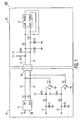
- FIG. 1 is a diagram of a relevant portion of an apparatus suitable for implementing the present invention
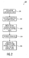
- FIG. 2 is a flowchart illustrating exemplary steps for practicing the present invention.
- FIG. 1 a diagram of a relevant portion of an apparatus 100 suitable for implementing the present invention is shown.
- apparatus 100 of FIG. 1 is represented as a television signal receiver.
- the principles of the present invention may be applicable to other types of electronic devices that use multiple circuit boards.
- Receiver 100 of FIG. 1 comprises a first circuit board 10, a second circuit board 20, and a board connector 30.
- first circuit board 10 enables operations related to power supply and deflection functions of receiver 100
- second circuit board 20 enables operations related to signal processing functions of receiver 100.
- First board 10 is electrically connected to second circuit board 20 via board connector 30.
- First circuit board 10 includes an electrically erasable, programmable read-only memory (“EEPROM”) 11 which operates as a non-volatile memory for storing data, such as voltage data used to control deflection operations of receiver 100.
- EEPROM 11 includes a clock (“CLK”) terminal and a data (“DAT”) terminal, and is powered by a voltage source V1, which according to the exemplary embodiment is 3.3 volts.
- CLK terminal is electrically coupled to a serial clock line (“SCL”) 13
- the DAT terminal is electrically coupled to a serial data line (“SDL”) 15.
- SCL 13 and SDL 15 collectively represent an inter-integrated circuit (“IIC” - typically pronounced "I-squared C”) bus, and may be referred to herein as bus lines or control lines.
- IIC inter-integrated circuit
- an IIC bus is a two transmission medium, bi-directional digital bus that permits two or more ICs to communicate on a bus path.
- An IC serving in a "master" mode of operation initiates a data transfer operation on the bus and generates clock signals that permit the data transfer.
- An IC serving in a "slave” mode of operation is the IC being operated on or communicated to by the master IC, whereby the slave IC is instructed to either send or receive data.
- Each IC has its own unique address, wherein the master IC initiates and terminates the communications. Further details regarding the IIC bus represented by SCL 13 and SDL 15 will be provided later herein.
- First circuit board 10 also includes eight resistors R1 to R8, two capacitors C1 and C2, and two transistors Q1 and Q2. Resistors R1 and R2 are provided to create resistance on SDL 15 and SCL 13, respectively. In the exemplary embodiment, resistors R1 and R2 each provide 1K ohms of resistance. As indicated in FIG. 1 , SCL 13 and SDL 15 are tapped in first circuit board 10 to provide two separate control channels. In particular, SDL 15 is tapped to provide a first control channel which generates an output signal represented at reference numeral 17, and SCL 13 is tapped to provide a second control channel which generates an output signal represented at reference numeral 19. Output signals 17 and 19 control deflection operations of receiver 100. The circuitry making up the first and second control channels may collectively be referred to herein as control circuitry.
- the first control channel includes resistors R3 to R5, capacitor C1, and transistor Q1.
- Resistor R3 provides a resistance between SDL 15 and the base junction of transistor Q1, and has a preferred value of 10K ohms.
- Transistor Q1 is preferably embodied as an n-type bipolar junction transistor ("BJT").
- BJT n-type bipolar junction transistor
- the collector junction of transistor Q1 provides an output path for the first control channel.
- Resistor R4 operates as a pull-up resistor and is electrically coupled to a voltage source V2, which according to an exemplary embodiment is 5.1 volts.
- the preferred value for resistor R4 is 1K ohms.
- Resistor R5 and capacitor C1 establish a time constant, and preferably have values of 1K ohms and 820 nanofarads, respectively.
- output signal 17 is used to establish the voltage of a flyback transformer (not shown), which is used in the deflection operations of receiver 100.
- the second control channel includes resistors R6 to R8, capacitor C2, and transistor Q2.
- Resistor R6 provides a resistance between SCL 13 and the base junction of transistor Q2, and has a preferred value of 10K ohms.
- Transistor Q2 is preferably embodied as an n-type BJT.
- the collector junction of transistor Q2 provides an output path for the second control channel.
- Resistor R7 operates as a pull-up resistor and is electrically coupled to voltage source V2, which as previously indicated is 5.1 volts.
- the preferred value for resistor R7 is 1K ohms.
- Resistor R8 and capacitor C2 establish a time constant, and preferably have values of 1K ohms and 820 nanofarads, respectively.
- output signal 19 is used to control the voltage of the flyback transformer (not shown).
- resistors R3 and R6 preferably are chosen to have sufficiently high resistances to prevent the loading of the IIC bus.
- Second circuit board 20 includes a microcontroller 21 which controls various operations of receiver 100. Like EEPROM 11 of first circuit board 10, microcontroller 21 also includes a CLK terminal and a DAT terminal. The CLK terminal is electrically coupled to SCL 13, and the DAT terminal is electrically coupled to SDL 15. Although not expressly shown in FIG. 1 , microcontroller 21 is electrically connected to a voltage source, such as voltage source V1.
- a voltage source such as voltage source V1.
- Microcontroller 21 also includes first and second pulse width modulated (“PWM”) terminals (“PWM1” and “PWM2”) which output first and second PWM signals, respectively.
- PWM1 and PWM2 terminals are electrically coupled to SDL 15 and SCL 13, respectively, and thereby provide the first and second PWM signals to the first and second control channels of first circuit board 10, respectively. Accordingly, the first PWM signal is used to generate output signal 17, and the second PWM signal is used to generate output signal 19. While PWM signals are utilized in a preferred embodiment, signals of other formats may, of course, also be utilized.
- Second circuit board 20 also includes four resistors R9 to R12, and two capacitors C3 and C4. Resistor R9 and capacitor C3 operate to filter out radio frequency interference from SDL 15, while resistor R10 and capacitor C4 operate to filter out radio frequency interference from SCL 13. According to an exemplary embodiment, resistors R9 and R10 each have values of 1K ohms, and capacitors C3 and C4 each have values of 100 picofarads. Resistors R11 and R12 operate as pull-up resistors and are electrically coupled to voltage source V1, which as previously indicated is 3.3 volts. Resistors R11 and R12 each have values of 10K ohms.
- the IIC bus (i.e., SCL 13 and SDL 15) is shared between two different operations of microcontroller 21.
- microcontroller 21 when receiver 100 is in a first operational state (i.e., receiver 100 is connected to a power source, but is in the OFF state), microcontroller 21 operates as a master IC and transmits first control signals to EEPROM 11 via SCL 13 and SDL 15 to thereby read data from EEPROM 11, which operates as a slave IC.
- the DAT pin is an input/output line and the CLK operates as an output pin.
- the PWM1 and PWM2 pins operate as input lines, or in a high impedance state.
- the state of the pins is determined by the microcontroller 21 in response to the current operational state, for example using the data directional registers.
- Microcontroller 21 and EEPROM 11 receive electrical power from a standby power source, namely voltage source V1, during the first operational state.
- the data read from EEPROM 11 by microcontroller 21 comprises voltage data used to control deflection operations of receiver 100.
- SCL 13 propagates clock signals from microcontroller 21 to EEPROM 11.
- SDL 15 is used to transfer data using serial digital transactions. Typically, one or more bits are used as acknowledgment bits.
- a transition from a logic low state to a logic high state on SDL 15, while SCL 13 is in a logic high state indicates a stop condition.
- microcontroller 21 generates one clock pulse for each bit of digital data transferred on SDL 15, and a logic state on SDL 15 can only change when the clock signal on SCL 13 is in a logic low state.
- signal protocols other than the foregoing one may be used.
- microcontroller 21 reads data from EEPROM 11, the PWM1 and PWM2 terminals of microcontroller 21 are in a high-impedance state, and resistors R3 and R6 prevent the control circuitry of the first and second control channels from loading SCL 13 and SDL 15.
- V2 applied to the collects of transistors Q1 and Q2 is in the low state, and thus, the application of signals to Q1 and Q2 does not have any effect on the control circuitry associated with terminals 17 and 19.
- the DAT and CLK terminals of microcontroller 21 are in a high-impedance state, and the PWM1 and PWM2 terminals may be used to output the first and second PWM signals, respectively.
- the first and second PWM signals may be referred to herein as second control signals.
- the PWM1 terminal is electrically coupled to SDL 15 and thereby provides the first PWM signal to the first control channel of first circuit board 10 to enable generation of output signal 17.
- the PWM2 terminal is electrically coupled to SCL 13 and thereby provides the second PWM signal to the second control channel of first circuit board 10 to enable generation of output signal 19.
- the first and second PWM signals are generated by microcontroller 21 in dependence upon the voltage data read from EEPROM 11 when receiver 100 is in an OFF state.
- SCL 13 and SDL 15 are shared between two different operations of microcontroller 21. Allowing the two lines to be shared between two different components that are used during two different operations, wherein different types of signals are transmitted during the two operations reduces the number of connectors required between boards 10 and 20.
- EEPROM 11 can be inadvertently written to and thereby corrupt data stored within EEPROM 11.
- a start condition i.e., a transition from a logic high state to a logic low state on SDL 15, while SCL 13 is in a logic high state
- address information generated by the phasing of the PWM signals corresponds to address information of EEPROM 11
- EEPROM 11 may be inadvertently written to by microprocessor 21. The potential for the occurrence of such signals that correspond to the above is unlikely.
- a given unit of data may be redundantly stored in five different memory locations of EEPROM 11.
- the component e.g., processor 21
- the component reading the data will apply a statistical threshold to determine whether the data has been corrupted. For example, if the data is stored in five different memory locations within EEPROM 11, the component reading the data may determine that the data is valid if three out of the five memory locations provide the same data.
- Other statistical thresholds may, of course, be employed.
- FIG. 2 a flowchart 200 illustrating exemplary steps for practicing the present invention is shown. For purposes of example and explanation, the steps of FIG. 2 will be described with reference to the television signal receiver 100 of FIG. 1 .
- receiver 100 is in an unpowered state. That is, receiver 100 is not connected to an electrical power source, such as a household plug outlet or the like.
- receiver 100 is connected to an electrical power source (e.g., plugged in), but is not turned ON. That is, receiver 100 enters the first operational state at step 202.
- an electrical power source e.g., plugged in
- certain components of receiver 100 such as microcontroller 21 and EEPROM 11 receive electrical power from a standby power source, namely voltage source V1, during the first operational state.
- step 203 receiver 100 performs an initialization process.
- microcontroller 21 operates as a master IC and transmits the first control signals to EEPROM 11 via SCL 13 and SDL 15 to thereby read data from EEPROM 11, which operates as a slave IC.
- the data read from EEPROM 11 by microcontroller 21 comprises voltage data used to control deflection operations of receiver 100.
- Microcontroller 21 stores the read data in an internal memory (not shown), and retains it there as long as receiver 100 is plugged in, or otherwise powered.
- receiver 100 is turned ON, for example, via a user input to an input terminal such as a hand-held remote control unit.
- receiver 100 is in the second operational state when it is both connected to a power source, and turned ON. Accordingly, step 204 causes receiver 100 to enter the second operational state.
- process flow advances to step 205 where microcontroller 21 transmits the second control signals, namely the first and second PWM signals, to the control circuitry of first circuit board 10. That is, the PWM1 terminal outputs the first PWM signal to SDL 15, and thereby provides the first PWM signal to the first control channel of first circuit board 10 to enable generation of output signal 17.
- the PWM2 terminal outputs the second PWM signal to SCL 13, and thereby provides the second PWM signal to the second control channel of first circuit board 10 to enable generation of output signal 19.
- the first and second PWM signals may be generated by microcontroller 21 in dependence upon the voltage data read from EEPROM 11 at step 203.
- SCL 13 and SDL 15 are shared between two different operations of microcontroller 21.
- the present invention has been described in relation to a television signal receiver, the invention is applicable to various systems, either with or without display devices, and the phrases "television signal receiver” or “receiver” as used herein are intended to encompass various types of apparatuses and systems including, but not limited to, television sets or monitors that include a display device, and systems or apparatuses such as a set-top box, video tape recorder (VTR), digital versatile disk (DVD) player, video game box, personal video recorder (PVR) or other apparatus that may not include a display device.
- VTR video tape recorder
- DVD digital versatile disk
- PVR personal video recorder
- control lines disclosed herein may be used in different operational states of an apparatus to control devices other than a memory or deflection circuitry.
- This application is therefore intended to cover any variations, uses, or adaptations of the invention, or departures from the present disclosure as come within known or customary practice in the art to which this invention pertains, which fall within the limits of the appended claims.
Landscapes
- Engineering & Computer Science (AREA)
- Multimedia (AREA)
- Signal Processing (AREA)
- General Engineering & Computer Science (AREA)
- Software Systems (AREA)
- Microelectronics & Electronic Packaging (AREA)
- Two-Way Televisions, Distribution Of Moving Picture Or The Like (AREA)
- Circuits Of Receivers In General (AREA)
- Electronic Switches (AREA)
- Selective Calling Equipment (AREA)
Applications Claiming Priority (3)
| Application Number | Priority Date | Filing Date | Title |
|---|---|---|---|
| US24981 | 1987-03-12 | ||
| US10/024,981 US6870578B2 (en) | 2001-12-19 | 2001-12-19 | Apparatus and method for sharing signal control lines |
| PCT/US2002/039503 WO2003055203A1 (en) | 2001-12-19 | 2002-12-11 | Apparatus and method for sharing signal control lines |
Publications (2)
| Publication Number | Publication Date |
|---|---|
| EP1457043A1 EP1457043A1 (en) | 2004-09-15 |
| EP1457043B1 true EP1457043B1 (en) | 2008-09-24 |
Family
ID=21823380
Family Applications (1)
| Application Number | Title | Priority Date | Filing Date |
|---|---|---|---|
| EP02786998A Expired - Lifetime EP1457043B1 (en) | 2001-12-19 | 2002-12-11 | Apparatus and method for sharing signal control lines |
Country Status (10)
| Country | Link |
|---|---|
| US (1) | US6870578B2 (enExample) |
| EP (1) | EP1457043B1 (enExample) |
| JP (1) | JP4260632B2 (enExample) |
| KR (1) | KR100922019B1 (enExample) |
| CN (1) | CN1276650C (enExample) |
| AU (1) | AU2002351345A1 (enExample) |
| DE (1) | DE60229069D1 (enExample) |
| MX (1) | MXPA04006064A (enExample) |
| MY (1) | MY136143A (enExample) |
| WO (1) | WO2003055203A1 (enExample) |
Families Citing this family (6)
| Publication number | Priority date | Publication date | Assignee | Title |
|---|---|---|---|---|
| US6563953B2 (en) | 1998-11-30 | 2003-05-13 | Microsoft Corporation | Predictive image compression using a single variable length code for both the luminance and chrominance blocks for each macroblock |
| WO2003053066A1 (en) | 2001-12-17 | 2003-06-26 | Microsoft Corporation | Skip macroblock coding |
| US8525931B2 (en) * | 2002-01-11 | 2013-09-03 | Thomson Licensing | Method and apparatus for isolating IIC bus noise from a tuner in a television receiver |
| KR100692529B1 (ko) * | 2005-07-01 | 2007-03-09 | 삼성전자주식회사 | 최적화된 딜레이 타임 결정 방법, 장치 및 최적화된 딜레이타임 결정 프로그램이 기록된 컴퓨터로 판독 가능한기록매체 |
| US9077960B2 (en) | 2005-08-12 | 2015-07-07 | Microsoft Corporation | Non-zero coefficient block pattern coding |
| JP4897073B2 (ja) * | 2010-06-30 | 2012-03-14 | 株式会社東芝 | 電源供給回路 |
Family Cites Families (6)
| Publication number | Priority date | Publication date | Assignee | Title |
|---|---|---|---|---|
| JPH0472970A (ja) * | 1990-07-13 | 1992-03-06 | Matsushita Electric Ind Co Ltd | シャーシ構造 |
| US5563655A (en) * | 1994-02-28 | 1996-10-08 | Eastman Kodak Company | Intelligent digital image storage for an electronic camera |
| US6151077A (en) * | 1994-12-22 | 2000-11-21 | U.S. Philips Corporation | Interface system for a television receiver |
| US5748255A (en) * | 1994-12-22 | 1998-05-05 | Philips Electronics North America Corporation | Interface system for a television receiver |
| US6437829B1 (en) * | 1997-01-16 | 2002-08-20 | Display Laboratories, Inc. | Alignment of cathode ray tube displays using a video graphics controller |
| US6693678B1 (en) * | 1997-12-18 | 2004-02-17 | Thomson Licensing S.A. | Data bus driver having first and second operating modes for coupling data to the bus at first and second rates |
-
2001
- 2001-12-19 US US10/024,981 patent/US6870578B2/en not_active Expired - Lifetime
-
2002
- 2002-12-11 CN CNB028257642A patent/CN1276650C/zh not_active Expired - Fee Related
- 2002-12-11 EP EP02786998A patent/EP1457043B1/en not_active Expired - Lifetime
- 2002-12-11 AU AU2002351345A patent/AU2002351345A1/en not_active Abandoned
- 2002-12-11 JP JP2003555795A patent/JP4260632B2/ja not_active Expired - Fee Related
- 2002-12-11 KR KR1020047009413A patent/KR100922019B1/ko not_active Expired - Fee Related
- 2002-12-11 WO PCT/US2002/039503 patent/WO2003055203A1/en not_active Ceased
- 2002-12-11 MX MXPA04006064A patent/MXPA04006064A/es active IP Right Grant
- 2002-12-11 DE DE60229069T patent/DE60229069D1/de not_active Expired - Lifetime
- 2002-12-18 MY MYPI20024763A patent/MY136143A/en unknown
Also Published As
| Publication number | Publication date |
|---|---|
| EP1457043A1 (en) | 2004-09-15 |
| US6870578B2 (en) | 2005-03-22 |
| CN1276650C (zh) | 2006-09-20 |
| KR20040068261A (ko) | 2004-07-30 |
| WO2003055203A1 (en) | 2003-07-03 |
| CN1606867A (zh) | 2005-04-13 |
| KR100922019B1 (ko) | 2009-10-19 |
| JP2005514814A (ja) | 2005-05-19 |
| AU2002351345A1 (en) | 2003-07-09 |
| MY136143A (en) | 2008-08-29 |
| US20030112375A1 (en) | 2003-06-19 |
| MXPA04006064A (es) | 2004-09-27 |
| JP4260632B2 (ja) | 2009-04-30 |
| DE60229069D1 (de) | 2008-11-06 |
Similar Documents
| Publication | Publication Date | Title |
|---|---|---|
| EP1457044B1 (en) | Apparatus and method for protecting a memory | |
| US20090096799A1 (en) | Display apparatus | |
| RU2649764C2 (ru) | Обнаружение периферийного usb-устройства на шине, не снабженной мощностью | |
| EP1457043B1 (en) | Apparatus and method for sharing signal control lines | |
| US8230151B2 (en) | Configurable data port for I2C or single-wire broadcast interface | |
| EP1290567B1 (en) | Bus operation with integrated circuits in an unpowered state | |
| US20050185665A1 (en) | Management method for a bidirectional and simultaneous exchange of digital signals and a corresponding interface for a bidirectional and simultaneous communication | |
| JP4037630B2 (ja) | デジタルav装置及びその制御方法 | |
| JP2009123284A (ja) | 電子機器 | |
| CN101164052A (zh) | 用于i2c或单线广播接口的可设置数据端口 | |
| JP2003135456A (ja) | 超音波診断装置 | |
| WO2009077964A1 (en) | Video interface |
Legal Events
| Date | Code | Title | Description |
|---|---|---|---|
| PUAI | Public reference made under article 153(3) epc to a published international application that has entered the european phase |
Free format text: ORIGINAL CODE: 0009012 |
|
| 17P | Request for examination filed |
Effective date: 20040605 |
|
| AK | Designated contracting states |
Kind code of ref document: A1 Designated state(s): AT BE BG CH CY CZ DE DK EE ES FI FR GB GR IE IT LI LU MC NL PT SE SI SK TR |
|
| AX | Request for extension of the european patent |
Extension state: AL LT LV MK RO |
|
| 17Q | First examination report despatched |
Effective date: 20041129 |
|
| RAP1 | Party data changed (applicant data changed or rights of an application transferred) |
Owner name: THOMSON LICENSING |
|
| GRAP | Despatch of communication of intention to grant a patent |
Free format text: ORIGINAL CODE: EPIDOSNIGR1 |
|
| GRAS | Grant fee paid |
Free format text: ORIGINAL CODE: EPIDOSNIGR3 |
|
| GRAA | (expected) grant |
Free format text: ORIGINAL CODE: 0009210 |
|
| AK | Designated contracting states |
Kind code of ref document: B1 Designated state(s): DE FR GB IT TR |
|
| REG | Reference to a national code |
Ref country code: GB Ref legal event code: FG4D |
|
| REF | Corresponds to: |
Ref document number: 60229069 Country of ref document: DE Date of ref document: 20081106 Kind code of ref document: P |
|
| REG | Reference to a national code |
Ref country code: GB Ref legal event code: 746 Effective date: 20081021 |
|
| PLBE | No opposition filed within time limit |
Free format text: ORIGINAL CODE: 0009261 |
|
| STAA | Information on the status of an ep patent application or granted ep patent |
Free format text: STATUS: NO OPPOSITION FILED WITHIN TIME LIMIT |
|
| PG25 | Lapsed in a contracting state [announced via postgrant information from national office to epo] |
Ref country code: IT Free format text: LAPSE BECAUSE OF FAILURE TO SUBMIT A TRANSLATION OF THE DESCRIPTION OR TO PAY THE FEE WITHIN THE PRESCRIBED TIME-LIMIT Effective date: 20080924 |
|
| 26N | No opposition filed |
Effective date: 20090625 |
|
| PG25 | Lapsed in a contracting state [announced via postgrant information from national office to epo] |
Ref country code: TR Free format text: LAPSE BECAUSE OF FAILURE TO SUBMIT A TRANSLATION OF THE DESCRIPTION OR TO PAY THE FEE WITHIN THE PRESCRIBED TIME-LIMIT Effective date: 20080924 |
|
| REG | Reference to a national code |
Ref country code: FR Ref legal event code: PLFP Year of fee payment: 14 |
|
| REG | Reference to a national code |
Ref country code: FR Ref legal event code: PLFP Year of fee payment: 15 |
|
| REG | Reference to a national code |
Ref country code: DE Ref legal event code: R082 Ref document number: 60229069 Country of ref document: DE Representative=s name: DEHNS, DE Ref country code: DE Ref legal event code: R082 Ref document number: 60229069 Country of ref document: DE Representative=s name: DEHNS PATENT AND TRADEMARK ATTORNEYS, DE Ref country code: DE Ref legal event code: R082 Ref document number: 60229069 Country of ref document: DE Representative=s name: HOFSTETTER, SCHURACK & PARTNER PATENT- UND REC, DE |
|
| REG | Reference to a national code |
Ref country code: FR Ref legal event code: PLFP Year of fee payment: 16 |
|
| REG | Reference to a national code |
Ref country code: FR Ref legal event code: TP Owner name: THOMSON LICENSING DTV, FR Effective date: 20180830 |
|
| REG | Reference to a national code |
Ref country code: GB Ref legal event code: 732E Free format text: REGISTERED BETWEEN 20180927 AND 20181005 |
|
| REG | Reference to a national code |
Ref country code: DE Ref legal event code: R082 Ref document number: 60229069 Country of ref document: DE Representative=s name: DEHNS, DE Ref country code: DE Ref legal event code: R081 Ref document number: 60229069 Country of ref document: DE Owner name: INTERDIGITAL MADISON PATENT HOLDINGS, FR Free format text: FORMER OWNER: THOMSON LICENSING, BOULOGNE-BILLANCOURT, FR Ref country code: DE Ref legal event code: R082 Ref document number: 60229069 Country of ref document: DE Representative=s name: DEHNS PATENT AND TRADEMARK ATTORNEYS, DE |
|
| PGFP | Annual fee paid to national office [announced via postgrant information from national office to epo] |
Ref country code: FR Payment date: 20191224 Year of fee payment: 18 |
|
| PGFP | Annual fee paid to national office [announced via postgrant information from national office to epo] |
Ref country code: DE Payment date: 20200131 Year of fee payment: 18 Ref country code: GB Payment date: 20191226 Year of fee payment: 18 |
|
| REG | Reference to a national code |
Ref country code: DE Ref legal event code: R119 Ref document number: 60229069 Country of ref document: DE |
|
| GBPC | Gb: european patent ceased through non-payment of renewal fee |
Effective date: 20201211 |
|
| PG25 | Lapsed in a contracting state [announced via postgrant information from national office to epo] |
Ref country code: FR Free format text: LAPSE BECAUSE OF NON-PAYMENT OF DUE FEES Effective date: 20201231 |
|
| PG25 | Lapsed in a contracting state [announced via postgrant information from national office to epo] |
Ref country code: GB Free format text: LAPSE BECAUSE OF NON-PAYMENT OF DUE FEES Effective date: 20201211 Ref country code: DE Free format text: LAPSE BECAUSE OF NON-PAYMENT OF DUE FEES Effective date: 20210701 |