EP1455451A2 - Dispositif de traitement de signal optique - Google Patents
Dispositif de traitement de signal optique Download PDFInfo
- Publication number
- EP1455451A2 EP1455451A2 EP04290499A EP04290499A EP1455451A2 EP 1455451 A2 EP1455451 A2 EP 1455451A2 EP 04290499 A EP04290499 A EP 04290499A EP 04290499 A EP04290499 A EP 04290499A EP 1455451 A2 EP1455451 A2 EP 1455451A2
- Authority
- EP
- European Patent Office
- Prior art keywords
- current
- value
- electronic component
- transistors
- diode
- Prior art date
- Legal status (The legal status is an assumption and is not a legal conclusion. Google has not performed a legal analysis and makes no representation as to the accuracy of the status listed.)
- Granted
Links
Images


Classifications
-
- H—ELECTRICITY
- H03—ELECTRONIC CIRCUITRY
- H03K—PULSE TECHNIQUE
- H03K5/00—Manipulating of pulses not covered by one of the other main groups of this subclass
- H03K5/01—Shaping pulses
- H03K5/08—Shaping pulses by limiting; by thresholding; by slicing, i.e. combined limiting and thresholding
-
- H—ELECTRICITY
- H03—ELECTRONIC CIRCUITRY
- H03F—AMPLIFIERS
- H03F3/00—Amplifiers with only discharge tubes or only semiconductor devices as amplifying elements
- H03F3/04—Amplifiers with only discharge tubes or only semiconductor devices as amplifying elements with semiconductor devices only
- H03F3/08—Amplifiers with only discharge tubes or only semiconductor devices as amplifying elements with semiconductor devices only controlled by light
-
- H—ELECTRICITY
- H04—ELECTRIC COMMUNICATION TECHNIQUE
- H04L—TRANSMISSION OF DIGITAL INFORMATION, e.g. TELEGRAPHIC COMMUNICATION
- H04L25/00—Baseband systems
- H04L25/02—Details ; arrangements for supplying electrical power along data transmission lines
- H04L25/06—DC level restoring means; Bias distortion correction ; Decision circuits providing symbol by symbol detection
Definitions
- the present invention relates to a signal processing device optical.
- This device is particularly suitable for producing a circuit decision in the field of very high optical signal transmission debit.
- Optical fiber with its broad bandwidth, is the preferred medium for transmissions to long distance.
- an optical signal is in the form of a carrier wave modulated between high logic levels, or “1”, and low levels, or logical "0", at the rate of a clock frequency which imposes the flow.
- the time allocated to contain binary information, or bit time, is so the clock period.
- An optoelectronic decision circuit makes it possible in particular to convert the successive levels of an optical signal with a certain delay modulated received which it is difficult to say if they correspond to "1" logic or logical “0”, into an easier digital electrical signal to interpret.
- phase margin in other words the ability to tolerate a time difference between the clock signal and the signal clock rate is crucial.
- this margin phase is necessarily reduced in high frequency operation, and therefore particularly at speeds of 80 Gbit / s, and it is particularly difficult to obtain, with a small margin of error, a clock front at a instant when a data signal modulated according to an RZ type format ("return to zero ”) is readable.
- the present invention aims to provide a device for processing a input signal having a RZ type format "return to zero" allowing to obtain an improved phase margin at high frequency.
- the control signal has a function of reset and corresponds to a pulse pulse train.
- the electronic component having a tunnel diode characteristic has a bistable configuration having two stable states A and B.
- the appearance of a control pulse forces the component into its stable state A. But, between two control pulses, if the input signal RZ has a high level, the component goes from an initial stable state A to the other stable state B; on the other hand, if the input signal has a low level, the component remains in its original state. Thanks to the invention, it suffices that the input signal take a high level corresponding to a logical "1" between two control pulses so that the component goes from state A to state B. taking sufficiently short control pulse durations by compared to bit time, we can considerably improve the margin of phase.
- said electronic component is a resonant tunneling diode.
- said electronic component is a photosensitive resonant tunneling diode which constitutes said means current generators.
- said current source comprises two transistors mounted in differential pair supplied by a fixed current, one said transistors being mounted in series with said electronic component.
- said current source comprises two transistors mounted in differential pair supplied by a fixed current, one of said transistors being a photosensitive transistor mounted in series with said electronic component, said photosensitive transistor constituting said current generating means.
- said modulation format of the data signal input having a given bit time is formed of voltage pulses of duration less than half bit time.
- the present invention also relates to a decision circuit for input data signal with RZ type modulation format "Return to zero" having a clock rate of given frequency, characterized in that it comprises a treatment device according to the invention, and in that said control signal consists of a pulse train having said given frequency.
- FIG. 1 represents a processing device 1 according to the invention.
- the bipolar transistors 3 and 4 are for example transistors bipolar heterojunction.
- the photosensitive resonant tunneling diode 2 is connected by its first terminal at a potential Vcc, usually zero, and by its second terminal at the collector of the bipolar transistor 3.
- Resistor 5 is connected by its first terminal to potential Vcc and by its second terminal at the collector of the bipolar transistor 4.
- Bipolar transistors 3 and 4 are mounted in differential pair and their transmitters are each connected to a common source of current I.
- the base of transistor 3 is fixed at a substantially constant potential V REF .
- V RESET is a pulse signal, the pulse duration being less than the duration of half a bit time.
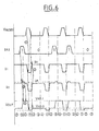
- V RESET-MAX is represented as a function of time in FIG. 6 and takes a value varying for example between 0 and a maximum value V RESET-MAX .
- the voltage V REF is a voltage strictly between 0 and V RESET-MAX , for example equal to V RESET-MAX / 2.
- the device 1 can be produced in the form of an integrated circuit.
- the document “InP-based monolithically integrated RTD / HBT mobile for logic circuits” (Otten et al., Conference Proceedings. 13 th IPRM, May 14-18, 2001, pages 232-235) describes how to integrate a diode resonant tunnel effect with a bipolar heterojunction transistor.
- Diode 2 receives an optical data signal E such as a signal optical clocked at a bit frequency for example of the order of 80 Gbit / s.
- the output voltage V OUT supplied by the device 1 is found at the collector of the transistor 3.
- I 1 the current flowing in transistor 3 and the diode 2 and I 2 the current flowing in transistor 4 and resistor 5.
- a pulse V RESET on the base of transistor 4 causes all the current I to flow in the right branch comprising the resistor 5 and the transistor 4.
- the current I 1 is therefore very low while the current I 2 is substantially equal to I
- the current flowing in the diode 2 is almost zero; the voltage across the diode 2 is almost zero and the output voltage V OUT is equal to V CC and is therefore substantially zero.
- This first state E 1 is illustrated in FIG. 2 which represents the current-voltage characteristics I 1 -V respective 6 and 7 of the diode 2 and of the transistor 3.
- the current-voltage characteristic 6 of the diode 2 is a conventional tunnel diode characteristic representing the current in the diode as a function of the voltage across its terminals; this characteristic has a peak current I p and a valley current I V.
- Characteristic 7 represents the characteristic of the collector of transistor 3 as a function of the voltage between the collector and the emitter of transistor 3. This characteristic is represented "upside down” with the origin at the polarization value; thus, at the crossroads of characteristics 6 and 7, there is indeed an equality of currents and a polarization.
- the current I supplies the left branch, and therefore the current I 1 is no longer zero and takes a value I R close to I, lower than the peak current I P.
- the device 1 is then in the state E 2 .
- Characteristic 8 represents the characteristic of the collector current of transistor 3 as a function of the voltage between the collector and the emitter of the transistor in the absence of a V RESET pulse.
- State E 2 is then defined by the intersection of characteristic 8 of transistor 3 and characteristic 6 of diode 2.
- the voltage across the diode 2 substantially equal to the voltage V OUT is equal to V RZ-0 located before the peak voltage of characteristic 6 corresponding to the peak current I P.
- the transistor I R and the diode 2 are crossed by the current I R lower than the peak current I P.
- This state E 2 is a stable operating state.
- the arrow 4 ⁇ designates the transition to a new stable state E 3 which is the only possible stable state.
- the voltage across the diode 2 which is substantially equal to V OUT is then equal to V RZ-1 greater than the voltage V RZ-0 .
- V RESET pulse makes it possible to switch the device back to the state E 1 .
- This passage is represented in FIG. 5 by the various arrows1 ⁇ .
- FIG. 6 represents the signals V RESET , I RZ , I 1 , I D and V out as a function of time.
- V OUT can take three values V CC , V RZ-0 and V RZ-1 corresponding respectively to the states E 1 , E 2 and E 3 .
- This voltage V OUT is the image shifted in time and improved by the light pulse E corresponding to the current I RZ .
- a current pulse I RZ corresponding to a logic "1" may give rise to a voltage pulse V OUT of duration greater than the duration of the pulse I RZ .
- bit half-times are represented by the duration separating two successive vertical lines. It is then clear that the smaller the pulse duration of V RESET before a half-bit time, the better the phase margin will be. In fact, the shorter the duration of the V RESET pulse, the more the current pulse I RZ is likely to occur between two V RESET pulses.
- the voltage-controlled current source including the pair differential of transistors 3 and 4 as shown in Figure 1 is given as an example and can be replaced by any type of current source voltage controlled.
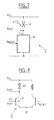
- Figure 7 shows the principle of embodiment of a device 1 'according to the invention. It is identical to the device as shown in FIG. 1 except that it includes any source of current 9 controlled by the voltage V RESET .
- FIG. 8 represents a third embodiment of a device 10 according to the invention.
- the device 10 is identical to the device as shown in the figure 1 except that diode 20 is a resonant tunneling diode non-photosensitive and that the bipolar transistor 30 is a transistor photosensitive. These differences aside, the functioning of the device 10 is similar to that described with reference to FIGS. 1 to 6.
Landscapes
- Engineering & Computer Science (AREA)
- Power Engineering (AREA)
- Physics & Mathematics (AREA)
- Nonlinear Science (AREA)
- Computer Networks & Wireless Communication (AREA)
- Signal Processing (AREA)
- Optical Communication System (AREA)
- Dc Digital Transmission (AREA)
- Electronic Switches (AREA)
- Silicon Polymers (AREA)
- Holo Graphy (AREA)
- Stabilization Of Oscillater, Synchronisation, Frequency Synthesizers (AREA)
Abstract
Description
- une source de courant commandée apte à injecter dans ledit composant électronique un courant électrique fonction d'un signal de commande, ledit courant pouvant prendre une première valeur de courant ou une deuxième valeur de courant,
- des moyens générateurs de courant aptes à injecter dans ledit composant électronique un courant électrique additionnel généré en réponse audit signal de données d'entrée,
- La figure 1 représente un premier mode de réalisation d'un dispositif de traitement selon l'invention,
- Les figures 2 à 5 représentent des caractéristiques courant-tension du dispositif représenté en figure 1,
- La figure 6 représente des chronogrammes de différents signaux de fonctionnement du dispositif représenté en figure 1,
- La figure 7 représente un deuxième mode de réalisation d'un dispositif de traitement selon l'invention,
- La figure 8 représente un troisième mode de réalisation d'un dispostif de traitement selon l'invention.
- une diode à effet tunnel résonnant photosensible 2,
- un premier transistor bipolaire 3,
- un deuxième transistor bipolaire 4,
- une résistance 5.
Claims (8)
- Dispositif (1) de traitement d'un signal optique de données (E) d'entrée ayant un format de modulation de type RZ « retour à zéro », comportant un composant électronique (2) ayant une caractéristique de diode tunnel présentant un courant de pic (IP) et un courant de vallée (IV), ledit dispositif (1) étant caractérisé en ce qu'il comporte :ledit courant de vallée (IV) ayant une valeur supérieure strictement à ladite première valeur de courant et ledit courant de pic (IP) ayant une valeur comprise entre ladite deuxième valeur de courant (IR) et la somme de ladite deuxième valeur de courant (IR) et de la valeur dudit courant généré (IRZ) par lesdits moyens générateurs (2).une source de courant (3, 4, 9) commandée apte à injecter dans ledit composant électronique (2) un courant électrique fonction d'un signal de commande (VRESET), ledit courant pouvant prendre une première valeur de courant ou une deuxième valeur de courant (IR),des moyens générateurs (2, 30) de courant aptes à injecter dans ledit composant électronique (2) un courant électrique additionnel (IRZ) généré en réponse audit signal de données d'entrée (E),
- Dispositif (1) selon la revendication 1, caractérisé en ce que ledit composant électronique (2, 20) est une diode à effet tunnel résonnant.
- Dispositif (1) selon la revendication 2, caractérisé en ce que ledit composant électronique (2) est une diode à effet tunnel résonnant photosensible qui constitue lesdits moyens générateurs de courant.
- Dispositif (1) selon l'une des revendications 1 à 3, caractérisé en ce que ladite source de courant comporte deux transistors (3, 4) montés en paire différentielle alimentée par un courant fixé (I), l'un desdits transistors (3) étant monté en série avec ledit composant électronique (2).
- Dispositif (10) selon l'une des revendications 1 ou 2, caractérisé en ce que ladite source de courant comporte deux transistors (3, 4) montés en paire différentielle alimentée par un courant fixé (I), l'un desdits transistors (30) étant un transistor photosensible monté en série avec ledit composant électronique (2), ledit transistor photosensible (30) constituant lesdits moyens générateurs de courant.
- Dispositif (1 ) selon l'une des revendications 1 à 5, caractérisé en ce que ledit format de modulation du signal de données (E) d'entrée présentant un temps bit donné, ledit signal de commande (VREF) est formé d'impulsions de tension de durée inférieure au demi temps bit.
- Circuit de décision pour signal de données (E) d'entrée ayant un format de modulation de type RZ « retour à zéro » présentant un rythme d'horloge de fréquence donnée, caractérisé en ce qu'il comprend un dispositif de traitement selon l'une des revendications 1 à 6, et en ce que ledit signal de commande (VRESET) est constitué d'un train d'impulsions ayant ladite fréquence donnée.
- Circuit intégré comportant un dispositif selon l'une des revendications 1 à 6.
Applications Claiming Priority (2)
| Application Number | Priority Date | Filing Date | Title |
|---|---|---|---|
| FR0302828A FR2852167B1 (fr) | 2003-03-07 | 2003-03-07 | Dispositif de correction de la phase d'un signal de donnees et circuit de decision associe |
| FR0302828 | 2003-03-07 |
Publications (3)
| Publication Number | Publication Date |
|---|---|
| EP1455451A2 true EP1455451A2 (fr) | 2004-09-08 |
| EP1455451A3 EP1455451A3 (fr) | 2008-11-05 |
| EP1455451B1 EP1455451B1 (fr) | 2009-11-11 |
Family
ID=32799646
Family Applications (1)
| Application Number | Title | Priority Date | Filing Date |
|---|---|---|---|
| EP04290499A Expired - Lifetime EP1455451B1 (fr) | 2003-03-07 | 2004-02-25 | Dispositif de traitement de signal optique |
Country Status (5)
| Country | Link |
|---|---|
| US (1) | US7015724B2 (fr) |
| EP (1) | EP1455451B1 (fr) |
| AT (1) | ATE448600T1 (fr) |
| DE (1) | DE602004023983D1 (fr) |
| FR (1) | FR2852167B1 (fr) |
Families Citing this family (3)
| Publication number | Priority date | Publication date | Assignee | Title |
|---|---|---|---|---|
| KR100719310B1 (ko) * | 2005-09-23 | 2007-05-17 | 한국과학기술원 | 셋/리셋 래치 회로, 시미트 트리거 회로 및 셋/리셋 래치회로를 이용한 모바일 기반의 d형 플립 플롭 회로와주파수 분배기 회로 |
| US8525553B1 (en) * | 2012-04-30 | 2013-09-03 | Hewlett-Packard Development Company, L.P. | Negative differential resistance comparator circuits |
| DE102012213172B4 (de) * | 2012-04-30 | 2018-01-04 | Rohde & Schwarz Gmbh & Co. Kg | Optisch getakteter Digital/Analog-Wandler und DDS-Einheit mit solchem Wandler |
Family Cites Families (9)
| Publication number | Priority date | Publication date | Assignee | Title |
|---|---|---|---|---|
| NL287685A (fr) * | 1962-01-26 | |||
| US3253165A (en) * | 1963-12-23 | 1966-05-24 | Rca Corp | Current steering logic circuit employing negative resistance devices in the output networks of the amplifying devices |
| US3456128A (en) * | 1965-12-22 | 1969-07-15 | Monsanto Co | Differential amplifier voltage comparison circuitry including a network for converting spurious normal mode signals to common mode signals |
| DE2337039C3 (de) * | 1973-07-20 | 1979-03-15 | Josef 7990 Friedrichshafen Wagner | Spritzpistole |
| US3889134A (en) * | 1974-05-16 | 1975-06-10 | Trw Inc | Tunnel diode digital data sample, decision and hold circuit |
| US5825240A (en) * | 1994-11-30 | 1998-10-20 | Massachusetts Institute Of Technology | Resonant-tunneling transmission line technology |
| US5773996A (en) * | 1995-05-22 | 1998-06-30 | Nippon Telegraph And Telephone Corporation | Multiple-valued logic circuit |
| US6362660B1 (en) * | 1999-07-13 | 2002-03-26 | Texas Instruments Incorporated | CMOS latch and register circuitry using quantum mechanical tunneling structures |
| US6316965B1 (en) * | 2000-06-15 | 2001-11-13 | The United States Of America As Represented By The Secretary Of The Navy | Non-volatile reprogrammable logic circuits by combining negative differential resistance devices and magnetic devices |
-
2003
- 2003-03-07 FR FR0302828A patent/FR2852167B1/fr not_active Expired - Fee Related
-
2004
- 2004-02-25 DE DE602004023983T patent/DE602004023983D1/de not_active Expired - Lifetime
- 2004-02-25 EP EP04290499A patent/EP1455451B1/fr not_active Expired - Lifetime
- 2004-02-25 AT AT04290499T patent/ATE448600T1/de not_active IP Right Cessation
- 2004-03-05 US US10/792,846 patent/US7015724B2/en not_active Expired - Fee Related
Also Published As
| Publication number | Publication date |
|---|---|
| ATE448600T1 (de) | 2009-11-15 |
| EP1455451B1 (fr) | 2009-11-11 |
| EP1455451A3 (fr) | 2008-11-05 |
| FR2852167B1 (fr) | 2006-07-14 |
| US20040174280A1 (en) | 2004-09-09 |
| DE602004023983D1 (de) | 2009-12-24 |
| US7015724B2 (en) | 2006-03-21 |
| FR2852167A1 (fr) | 2004-09-10 |
Similar Documents
| Publication | Publication Date | Title |
|---|---|---|
| EP0181664B1 (fr) | Comparateur synchronisé | |
| EP3134972B1 (fr) | Cellule de commutation de puissance a transistors a effet de champ de type normalement conducteur | |
| EP1085659A1 (fr) | Convertisseur numérique-analogique en courant | |
| FR2534746A1 (fr) | Emetteur laser et procede pour le faire fonctionner | |
| FR2702317A1 (fr) | Circuit pompe de charge à faible consommation, faible bruit et synthétiseur de fréquence équipé d'un tel circuit. | |
| EP0029767A1 (fr) | Procédé de commande d'un montage Darlington et montage Darlington à faibles pertes | |
| FR2594275A1 (fr) | Circuit de decalage de niveau pour un convertisseur serie-parallele | |
| EP1455451B1 (fr) | Dispositif de traitement de signal optique | |
| EP0561456B1 (fr) | Miroir de courant à commutation accélérée | |
| FR2520174A1 (fr) | Systeme de transmission de signaux numeriques sur fibre optique | |
| EP0011534B1 (fr) | Procédé et dispositif de traitement d'un signal analogique, notamment pseudopériodique | |
| FR2695215A1 (fr) | Tête optique d'émission-réception pour transmission de données par système optique, et circuit de commutation pour cette tête. | |
| FR3029041A1 (fr) | Recepteur optique muni d'un bloc de controle de seuil | |
| FR2681993A1 (fr) | Circuit de source de courant a transistors ayant des types de conductivite differents et procede pour faire fonctionner ce circuit. | |
| FR2480047A1 (fr) | Amplificateur a double mode de fonctionnement, lineaire et non lineaire | |
| EP0981203B1 (fr) | Source de courant contrôlée à commutation accélérée | |
| WO2007000387A1 (fr) | Commutateur de courant a paire differentielle de transistors alimente par une faible tension vcc | |
| FR2508746A1 (fr) | Capteur d'image | |
| EP0099956B1 (fr) | Récepteur de signaux et son utilisation dans un circuit de réception indiquant l'état de l'équipement connecté | |
| FR2477802A1 (fr) | Circuit d'amplification | |
| EP0534866A1 (fr) | Interrupteur statique à faibles pertes | |
| EP1499042A1 (fr) | Codeur différentiel de signaux électriques | |
| EP0760180B1 (fr) | Procede et dispositif de commutation pseudo-aleatoire | |
| FR2881850A1 (fr) | Circuit de generation d'une tension de reference flottante, en technologie cmos | |
| EP1211808A1 (fr) | Dispositif de modulation de la largeur d'impulsion de signaux très hautes fréquences |
Legal Events
| Date | Code | Title | Description |
|---|---|---|---|
| PUAI | Public reference made under article 153(3) epc to a published international application that has entered the european phase |
Free format text: ORIGINAL CODE: 0009012 |
|
| AK | Designated contracting states |
Kind code of ref document: A2 Designated state(s): AT BE BG CH CY CZ DE DK EE ES FI FR GB GR HU IE IT LI LU MC NL PT RO SE SI SK TR |
|
| AX | Request for extension of the european patent |
Extension state: AL HR LT LV MK |
|
| RAP1 | Party data changed (applicant data changed or rights of an application transferred) |
Owner name: ALCATEL LUCENT |
|
| PUAL | Search report despatched |
Free format text: ORIGINAL CODE: 0009013 |
|
| AK | Designated contracting states |
Kind code of ref document: A3 Designated state(s): AT BE BG CH CY CZ DE DK EE ES FI FR GB GR HU IE IT LI LU MC NL PT RO SE SI SK TR |
|
| AX | Request for extension of the european patent |
Extension state: AL LT LV MK |
|
| 17P | Request for examination filed |
Effective date: 20090311 |
|
| GRAP | Despatch of communication of intention to grant a patent |
Free format text: ORIGINAL CODE: EPIDOSNIGR1 |
|
| AKX | Designation fees paid |
Designated state(s): AT BE BG CH CY CZ DE DK EE ES FI FR GB GR HU IE IT LI LU MC NL PT RO SE SI SK TR |
|
| GRAS | Grant fee paid |
Free format text: ORIGINAL CODE: EPIDOSNIGR3 |
|
| GRAA | (expected) grant |
Free format text: ORIGINAL CODE: 0009210 |
|
| AK | Designated contracting states |
Kind code of ref document: B1 Designated state(s): AT BE BG CH CY CZ DE DK EE ES FI FR GB GR HU IE IT LI LU MC NL PT RO SE SI SK TR |
|
| REG | Reference to a national code |
Ref country code: GB Ref legal event code: FG4D Free format text: NOT ENGLISH |
|
| REG | Reference to a national code |
Ref country code: CH Ref legal event code: EP |
|
| REG | Reference to a national code |
Ref country code: IE Ref legal event code: FG4D |
|
| REF | Corresponds to: |
Ref document number: 602004023983 Country of ref document: DE Date of ref document: 20091224 Kind code of ref document: P |
|
| NLV1 | Nl: lapsed or annulled due to failure to fulfill the requirements of art. 29p and 29m of the patents act | ||
| PG25 | Lapsed in a contracting state [announced via postgrant information from national office to epo] |
Ref country code: PT Free format text: LAPSE BECAUSE OF FAILURE TO SUBMIT A TRANSLATION OF THE DESCRIPTION OR TO PAY THE FEE WITHIN THE PRESCRIBED TIME-LIMIT Effective date: 20100311 Ref country code: ES Free format text: LAPSE BECAUSE OF FAILURE TO SUBMIT A TRANSLATION OF THE DESCRIPTION OR TO PAY THE FEE WITHIN THE PRESCRIBED TIME-LIMIT Effective date: 20100222 Ref country code: SE Free format text: LAPSE BECAUSE OF FAILURE TO SUBMIT A TRANSLATION OF THE DESCRIPTION OR TO PAY THE FEE WITHIN THE PRESCRIBED TIME-LIMIT Effective date: 20091111 Ref country code: FI Free format text: LAPSE BECAUSE OF FAILURE TO SUBMIT A TRANSLATION OF THE DESCRIPTION OR TO PAY THE FEE WITHIN THE PRESCRIBED TIME-LIMIT Effective date: 20091111 |
|
| PG25 | Lapsed in a contracting state [announced via postgrant information from national office to epo] |
Ref country code: SI Free format text: LAPSE BECAUSE OF FAILURE TO SUBMIT A TRANSLATION OF THE DESCRIPTION OR TO PAY THE FEE WITHIN THE PRESCRIBED TIME-LIMIT Effective date: 20091111 Ref country code: CY Free format text: LAPSE BECAUSE OF FAILURE TO SUBMIT A TRANSLATION OF THE DESCRIPTION OR TO PAY THE FEE WITHIN THE PRESCRIBED TIME-LIMIT Effective date: 20091111 |
|
| REG | Reference to a national code |
Ref country code: IE Ref legal event code: FD4D |
|
| PG25 | Lapsed in a contracting state [announced via postgrant information from national office to epo] |
Ref country code: AT Free format text: LAPSE BECAUSE OF FAILURE TO SUBMIT A TRANSLATION OF THE DESCRIPTION OR TO PAY THE FEE WITHIN THE PRESCRIBED TIME-LIMIT Effective date: 20091111 |
|
| PG25 | Lapsed in a contracting state [announced via postgrant information from national office to epo] |
Ref country code: BG Free format text: LAPSE BECAUSE OF FAILURE TO SUBMIT A TRANSLATION OF THE DESCRIPTION OR TO PAY THE FEE WITHIN THE PRESCRIBED TIME-LIMIT Effective date: 20100211 Ref country code: IE Free format text: LAPSE BECAUSE OF FAILURE TO SUBMIT A TRANSLATION OF THE DESCRIPTION OR TO PAY THE FEE WITHIN THE PRESCRIBED TIME-LIMIT Effective date: 20091111 Ref country code: DK Free format text: LAPSE BECAUSE OF FAILURE TO SUBMIT A TRANSLATION OF THE DESCRIPTION OR TO PAY THE FEE WITHIN THE PRESCRIBED TIME-LIMIT Effective date: 20091111 Ref country code: EE Free format text: LAPSE BECAUSE OF FAILURE TO SUBMIT A TRANSLATION OF THE DESCRIPTION OR TO PAY THE FEE WITHIN THE PRESCRIBED TIME-LIMIT Effective date: 20091111 Ref country code: RO Free format text: LAPSE BECAUSE OF FAILURE TO SUBMIT A TRANSLATION OF THE DESCRIPTION OR TO PAY THE FEE WITHIN THE PRESCRIBED TIME-LIMIT Effective date: 20091111 |
|
| BERE | Be: lapsed |
Owner name: ALCATEL LUCENT Effective date: 20100228 |
|
| PG25 | Lapsed in a contracting state [announced via postgrant information from national office to epo] |
Ref country code: SK Free format text: LAPSE BECAUSE OF FAILURE TO SUBMIT A TRANSLATION OF THE DESCRIPTION OR TO PAY THE FEE WITHIN THE PRESCRIBED TIME-LIMIT Effective date: 20091111 Ref country code: CZ Free format text: LAPSE BECAUSE OF FAILURE TO SUBMIT A TRANSLATION OF THE DESCRIPTION OR TO PAY THE FEE WITHIN THE PRESCRIBED TIME-LIMIT Effective date: 20091111 |
|
| PLBE | No opposition filed within time limit |
Free format text: ORIGINAL CODE: 0009261 |
|
| STAA | Information on the status of an ep patent application or granted ep patent |
Free format text: STATUS: NO OPPOSITION FILED WITHIN TIME LIMIT |
|
| REG | Reference to a national code |
Ref country code: CH Ref legal event code: PL |
|
| 26N | No opposition filed |
Effective date: 20100812 |
|
| PG25 | Lapsed in a contracting state [announced via postgrant information from national office to epo] |
Ref country code: MC Free format text: LAPSE BECAUSE OF NON-PAYMENT OF DUE FEES Effective date: 20100301 Ref country code: LI Free format text: LAPSE BECAUSE OF NON-PAYMENT OF DUE FEES Effective date: 20100228 Ref country code: CH Free format text: LAPSE BECAUSE OF NON-PAYMENT OF DUE FEES Effective date: 20100228 Ref country code: GR Free format text: LAPSE BECAUSE OF FAILURE TO SUBMIT A TRANSLATION OF THE DESCRIPTION OR TO PAY THE FEE WITHIN THE PRESCRIBED TIME-LIMIT Effective date: 20100212 |
|
| PG25 | Lapsed in a contracting state [announced via postgrant information from national office to epo] |
Ref country code: BE Free format text: LAPSE BECAUSE OF NON-PAYMENT OF DUE FEES Effective date: 20100228 |
|
| PG25 | Lapsed in a contracting state [announced via postgrant information from national office to epo] |
Ref country code: IT Free format text: LAPSE BECAUSE OF FAILURE TO SUBMIT A TRANSLATION OF THE DESCRIPTION OR TO PAY THE FEE WITHIN THE PRESCRIBED TIME-LIMIT Effective date: 20091111 |
|
| PG25 | Lapsed in a contracting state [announced via postgrant information from national office to epo] |
Ref country code: HU Free format text: LAPSE BECAUSE OF FAILURE TO SUBMIT A TRANSLATION OF THE DESCRIPTION OR TO PAY THE FEE WITHIN THE PRESCRIBED TIME-LIMIT Effective date: 20100512 Ref country code: LU Free format text: LAPSE BECAUSE OF NON-PAYMENT OF DUE FEES Effective date: 20100225 Ref country code: NL Free format text: LAPSE BECAUSE OF FAILURE TO SUBMIT A TRANSLATION OF THE DESCRIPTION OR TO PAY THE FEE WITHIN THE PRESCRIBED TIME-LIMIT Effective date: 20091111 |
|
| PG25 | Lapsed in a contracting state [announced via postgrant information from national office to epo] |
Ref country code: TR Free format text: LAPSE BECAUSE OF FAILURE TO SUBMIT A TRANSLATION OF THE DESCRIPTION OR TO PAY THE FEE WITHIN THE PRESCRIBED TIME-LIMIT Effective date: 20091111 |
|
| REG | Reference to a national code |
Ref country code: FR Ref legal event code: GC Effective date: 20131018 |
|
| REG | Reference to a national code |
Ref country code: FR Ref legal event code: RG Effective date: 20141016 |
|
| REG | Reference to a national code |
Ref country code: FR Ref legal event code: PLFP Year of fee payment: 12 |
|
| REG | Reference to a national code |
Ref country code: FR Ref legal event code: CA Effective date: 20150521 |
|
| REG | Reference to a national code |
Ref country code: FR Ref legal event code: CA Effective date: 20150521 |
|
| REG | Reference to a national code |
Ref country code: FR Ref legal event code: PLFP Year of fee payment: 13 |
|
| REG | Reference to a national code |
Ref country code: FR Ref legal event code: PLFP Year of fee payment: 14 |
|
| PGFP | Annual fee paid to national office [announced via postgrant information from national office to epo] |
Ref country code: FR Payment date: 20170217 Year of fee payment: 14 Ref country code: DE Payment date: 20170217 Year of fee payment: 14 |
|
| PGFP | Annual fee paid to national office [announced via postgrant information from national office to epo] |
Ref country code: GB Payment date: 20170216 Year of fee payment: 14 |
|
| REG | Reference to a national code |
Ref country code: DE Ref legal event code: R119 Ref document number: 602004023983 Country of ref document: DE |
|
| GBPC | Gb: european patent ceased through non-payment of renewal fee |
Effective date: 20180225 |
|
| REG | Reference to a national code |
Ref country code: FR Ref legal event code: ST Effective date: 20181031 |
|
| PG25 | Lapsed in a contracting state [announced via postgrant information from national office to epo] |
Ref country code: DE Free format text: LAPSE BECAUSE OF NON-PAYMENT OF DUE FEES Effective date: 20180901 |
|
| PG25 | Lapsed in a contracting state [announced via postgrant information from national office to epo] |
Ref country code: FR Free format text: LAPSE BECAUSE OF NON-PAYMENT OF DUE FEES Effective date: 20180228 Ref country code: GB Free format text: LAPSE BECAUSE OF NON-PAYMENT OF DUE FEES Effective date: 20180225 |