EP1455392A1 - Semiconductor device and method for manufacturing the same - Google Patents
Semiconductor device and method for manufacturing the same Download PDFInfo
- Publication number
- EP1455392A1 EP1455392A1 EP01274912A EP01274912A EP1455392A1 EP 1455392 A1 EP1455392 A1 EP 1455392A1 EP 01274912 A EP01274912 A EP 01274912A EP 01274912 A EP01274912 A EP 01274912A EP 1455392 A1 EP1455392 A1 EP 1455392A1
- Authority
- EP
- European Patent Office
- Prior art keywords
- semiconductor device
- terminal
- insulating layer
- semiconductor chip
- semiconductor
- Prior art date
- Legal status (The legal status is an assumption and is not a legal conclusion. Google has not performed a legal analysis and makes no representation as to the accuracy of the status listed.)
- Ceased
Links
Images





Classifications
-
- H—ELECTRICITY
- H10—SEMICONDUCTOR DEVICES; ELECTRIC SOLID-STATE DEVICES NOT OTHERWISE PROVIDED FOR
- H10W—GENERIC PACKAGES, INTERCONNECTIONS, CONNECTORS OR OTHER CONSTRUCTIONAL DETAILS OF DEVICES COVERED BY CLASS H10
- H10W70/00—Package substrates; Interposers; Redistribution layers [RDL]
- H10W70/01—Manufacture or treatment
- H10W70/05—Manufacture or treatment of insulating or insulated package substrates, or of interposers, or of redistribution layers
- H10W70/08—Manufacture or treatment of insulating or insulated package substrates, or of interposers, or of redistribution layers by depositing layers on the chip or wafer, e.g. "chip-first" RDLs
- H10W70/09—Manufacture or treatment of insulating or insulated package substrates, or of interposers, or of redistribution layers by depositing layers on the chip or wafer, e.g. "chip-first" RDLs extending onto an encapsulation that laterally surrounds the chip or wafer, e.g. fan-out wafer level package [FOWLP] RDLs
-
- H—ELECTRICITY
- H10—SEMICONDUCTOR DEVICES; ELECTRIC SOLID-STATE DEVICES NOT OTHERWISE PROVIDED FOR
- H10W—GENERIC PACKAGES, INTERCONNECTIONS, CONNECTORS OR OTHER CONSTRUCTIONAL DETAILS OF DEVICES COVERED BY CLASS H10
- H10W70/00—Package substrates; Interposers; Redistribution layers [RDL]
- H10W70/60—Insulating or insulated package substrates; Interposers; Redistribution layers
-
- H—ELECTRICITY
- H10—SEMICONDUCTOR DEVICES; ELECTRIC SOLID-STATE DEVICES NOT OTHERWISE PROVIDED FOR
- H10W—GENERIC PACKAGES, INTERCONNECTIONS, CONNECTORS OR OTHER CONSTRUCTIONAL DETAILS OF DEVICES COVERED BY CLASS H10
- H10W70/00—Package substrates; Interposers; Redistribution layers [RDL]
- H10W70/60—Insulating or insulated package substrates; Interposers; Redistribution layers
- H10W70/611—Insulating or insulated package substrates; Interposers; Redistribution layers for connecting multiple chips together
- H10W70/614—Insulating or insulated package substrates; Interposers; Redistribution layers for connecting multiple chips together the multiple chips being integrally enclosed
-
- H—ELECTRICITY
- H10—SEMICONDUCTOR DEVICES; ELECTRIC SOLID-STATE DEVICES NOT OTHERWISE PROVIDED FOR
- H10W—GENERIC PACKAGES, INTERCONNECTIONS, CONNECTORS OR OTHER CONSTRUCTIONAL DETAILS OF DEVICES COVERED BY CLASS H10
- H10W72/00—Interconnections or connectors in packages
-
- H—ELECTRICITY
- H10—SEMICONDUCTOR DEVICES; ELECTRIC SOLID-STATE DEVICES NOT OTHERWISE PROVIDED FOR
- H10W—GENERIC PACKAGES, INTERCONNECTIONS, CONNECTORS OR OTHER CONSTRUCTIONAL DETAILS OF DEVICES COVERED BY CLASS H10
- H10W74/00—Encapsulations, e.g. protective coatings
- H10W74/10—Encapsulations, e.g. protective coatings characterised by their shape or disposition
-
- H—ELECTRICITY
- H10—SEMICONDUCTOR DEVICES; ELECTRIC SOLID-STATE DEVICES NOT OTHERWISE PROVIDED FOR
- H10W—GENERIC PACKAGES, INTERCONNECTIONS, CONNECTORS OR OTHER CONSTRUCTIONAL DETAILS OF DEVICES COVERED BY CLASS H10
- H10W74/00—Encapsulations, e.g. protective coatings
- H10W74/10—Encapsulations, e.g. protective coatings characterised by their shape or disposition
- H10W74/111—Encapsulations, e.g. protective coatings characterised by their shape or disposition the semiconductor body being completely enclosed
- H10W74/129—Encapsulations, e.g. protective coatings characterised by their shape or disposition the semiconductor body being completely enclosed forming a chip-scale package [CSP]
-
- H—ELECTRICITY
- H10—SEMICONDUCTOR DEVICES; ELECTRIC SOLID-STATE DEVICES NOT OTHERWISE PROVIDED FOR
- H10W—GENERIC PACKAGES, INTERCONNECTIONS, CONNECTORS OR OTHER CONSTRUCTIONAL DETAILS OF DEVICES COVERED BY CLASS H10
- H10W90/00—Package configurations
-
- H—ELECTRICITY
- H10—SEMICONDUCTOR DEVICES; ELECTRIC SOLID-STATE DEVICES NOT OTHERWISE PROVIDED FOR
- H10W—GENERIC PACKAGES, INTERCONNECTIONS, CONNECTORS OR OTHER CONSTRUCTIONAL DETAILS OF DEVICES COVERED BY CLASS H10
- H10W70/00—Package substrates; Interposers; Redistribution layers [RDL]
- H10W70/01—Manufacture or treatment
- H10W70/05—Manufacture or treatment of insulating or insulated package substrates, or of interposers, or of redistribution layers
- H10W70/093—Connecting or disconnecting other interconnections thereto or therefrom, e.g. connecting bond wires or bumps
-
- H—ELECTRICITY
- H10—SEMICONDUCTOR DEVICES; ELECTRIC SOLID-STATE DEVICES NOT OTHERWISE PROVIDED FOR
- H10W—GENERIC PACKAGES, INTERCONNECTIONS, CONNECTORS OR OTHER CONSTRUCTIONAL DETAILS OF DEVICES COVERED BY CLASS H10
- H10W70/00—Package substrates; Interposers; Redistribution layers [RDL]
- H10W70/099—Connecting interconnections to insulating or insulated package substrates, interposers or redistribution layers
-
- H—ELECTRICITY
- H10—SEMICONDUCTOR DEVICES; ELECTRIC SOLID-STATE DEVICES NOT OTHERWISE PROVIDED FOR
- H10W—GENERIC PACKAGES, INTERCONNECTIONS, CONNECTORS OR OTHER CONSTRUCTIONAL DETAILS OF DEVICES COVERED BY CLASS H10
- H10W70/00—Package substrates; Interposers; Redistribution layers [RDL]
- H10W70/60—Insulating or insulated package substrates; Interposers; Redistribution layers
- H10W70/62—Insulating or insulated package substrates; Interposers; Redistribution layers characterised by their interconnections
- H10W70/65—Shapes or dispositions of interconnections
- H10W70/654—Top-view layouts
- H10W70/655—Fan-out layouts
-
- H—ELECTRICITY
- H10—SEMICONDUCTOR DEVICES; ELECTRIC SOLID-STATE DEVICES NOT OTHERWISE PROVIDED FOR
- H10W—GENERIC PACKAGES, INTERCONNECTIONS, CONNECTORS OR OTHER CONSTRUCTIONAL DETAILS OF DEVICES COVERED BY CLASS H10
- H10W72/00—Interconnections or connectors in packages
- H10W72/01—Manufacture or treatment
- H10W72/012—Manufacture or treatment of bump connectors, dummy bumps or thermal bumps
-
- H—ELECTRICITY
- H10—SEMICONDUCTOR DEVICES; ELECTRIC SOLID-STATE DEVICES NOT OTHERWISE PROVIDED FOR
- H10W—GENERIC PACKAGES, INTERCONNECTIONS, CONNECTORS OR OTHER CONSTRUCTIONAL DETAILS OF DEVICES COVERED BY CLASS H10
- H10W72/00—Interconnections or connectors in packages
- H10W72/01—Manufacture or treatment
- H10W72/019—Manufacture or treatment of bond pads
-
- H—ELECTRICITY
- H10—SEMICONDUCTOR DEVICES; ELECTRIC SOLID-STATE DEVICES NOT OTHERWISE PROVIDED FOR
- H10W—GENERIC PACKAGES, INTERCONNECTIONS, CONNECTORS OR OTHER CONSTRUCTIONAL DETAILS OF DEVICES COVERED BY CLASS H10
- H10W72/00—Interconnections or connectors in packages
- H10W72/01—Manufacture or treatment
- H10W72/0198—Manufacture or treatment batch processes
-
- H—ELECTRICITY
- H10—SEMICONDUCTOR DEVICES; ELECTRIC SOLID-STATE DEVICES NOT OTHERWISE PROVIDED FOR
- H10W—GENERIC PACKAGES, INTERCONNECTIONS, CONNECTORS OR OTHER CONSTRUCTIONAL DETAILS OF DEVICES COVERED BY CLASS H10
- H10W72/00—Interconnections or connectors in packages
- H10W72/071—Connecting or disconnecting
- H10W72/073—Connecting or disconnecting of die-attach connectors
-
- H—ELECTRICITY
- H10—SEMICONDUCTOR DEVICES; ELECTRIC SOLID-STATE DEVICES NOT OTHERWISE PROVIDED FOR
- H10W—GENERIC PACKAGES, INTERCONNECTIONS, CONNECTORS OR OTHER CONSTRUCTIONAL DETAILS OF DEVICES COVERED BY CLASS H10
- H10W72/00—Interconnections or connectors in packages
- H10W72/20—Bump connectors, e.g. solder bumps or copper pillars; Dummy bumps; Thermal bumps
- H10W72/241—Dispositions, e.g. layouts
-
- H—ELECTRICITY
- H10—SEMICONDUCTOR DEVICES; ELECTRIC SOLID-STATE DEVICES NOT OTHERWISE PROVIDED FOR
- H10W—GENERIC PACKAGES, INTERCONNECTIONS, CONNECTORS OR OTHER CONSTRUCTIONAL DETAILS OF DEVICES COVERED BY CLASS H10
- H10W72/00—Interconnections or connectors in packages
- H10W72/20—Bump connectors, e.g. solder bumps or copper pillars; Dummy bumps; Thermal bumps
- H10W72/241—Dispositions, e.g. layouts
- H10W72/244—Dispositions, e.g. layouts relative to underlying supporting features, e.g. bond pads, RDLs or vias
-
- H—ELECTRICITY
- H10—SEMICONDUCTOR DEVICES; ELECTRIC SOLID-STATE DEVICES NOT OTHERWISE PROVIDED FOR
- H10W—GENERIC PACKAGES, INTERCONNECTIONS, CONNECTORS OR OTHER CONSTRUCTIONAL DETAILS OF DEVICES COVERED BY CLASS H10
- H10W72/00—Interconnections or connectors in packages
- H10W72/20—Bump connectors, e.g. solder bumps or copper pillars; Dummy bumps; Thermal bumps
- H10W72/251—Materials
-
- H—ELECTRICITY
- H10—SEMICONDUCTOR DEVICES; ELECTRIC SOLID-STATE DEVICES NOT OTHERWISE PROVIDED FOR
- H10W—GENERIC PACKAGES, INTERCONNECTIONS, CONNECTORS OR OTHER CONSTRUCTIONAL DETAILS OF DEVICES COVERED BY CLASS H10
- H10W72/00—Interconnections or connectors in packages
- H10W72/20—Bump connectors, e.g. solder bumps or copper pillars; Dummy bumps; Thermal bumps
- H10W72/251—Materials
- H10W72/252—Materials comprising solid metals or solid metalloids, e.g. PbSn, Ag or Cu
-
- H—ELECTRICITY
- H10—SEMICONDUCTOR DEVICES; ELECTRIC SOLID-STATE DEVICES NOT OTHERWISE PROVIDED FOR
- H10W—GENERIC PACKAGES, INTERCONNECTIONS, CONNECTORS OR OTHER CONSTRUCTIONAL DETAILS OF DEVICES COVERED BY CLASS H10
- H10W72/00—Interconnections or connectors in packages
- H10W72/20—Bump connectors, e.g. solder bumps or copper pillars; Dummy bumps; Thermal bumps
- H10W72/29—Bond pads specially adapted therefor
-
- H—ELECTRICITY
- H10—SEMICONDUCTOR DEVICES; ELECTRIC SOLID-STATE DEVICES NOT OTHERWISE PROVIDED FOR
- H10W—GENERIC PACKAGES, INTERCONNECTIONS, CONNECTORS OR OTHER CONSTRUCTIONAL DETAILS OF DEVICES COVERED BY CLASS H10
- H10W72/00—Interconnections or connectors in packages
- H10W72/50—Bond wires
- H10W72/551—Materials of bond wires
- H10W72/552—Materials of bond wires comprising metals or metalloids, e.g. silver
- H10W72/5522—Materials of bond wires comprising metals or metalloids, e.g. silver comprising gold [Au]
-
- H—ELECTRICITY
- H10—SEMICONDUCTOR DEVICES; ELECTRIC SOLID-STATE DEVICES NOT OTHERWISE PROVIDED FOR
- H10W—GENERIC PACKAGES, INTERCONNECTIONS, CONNECTORS OR OTHER CONSTRUCTIONAL DETAILS OF DEVICES COVERED BY CLASS H10
- H10W72/00—Interconnections or connectors in packages
- H10W72/50—Bond wires
- H10W72/59—Bond pads specially adapted therefor
-
- H—ELECTRICITY
- H10—SEMICONDUCTOR DEVICES; ELECTRIC SOLID-STATE DEVICES NOT OTHERWISE PROVIDED FOR
- H10W—GENERIC PACKAGES, INTERCONNECTIONS, CONNECTORS OR OTHER CONSTRUCTIONAL DETAILS OF DEVICES COVERED BY CLASS H10
- H10W72/00—Interconnections or connectors in packages
- H10W72/851—Dispositions of multiple connectors or interconnections
- H10W72/853—On the same surface
-
- H—ELECTRICITY
- H10—SEMICONDUCTOR DEVICES; ELECTRIC SOLID-STATE DEVICES NOT OTHERWISE PROVIDED FOR
- H10W—GENERIC PACKAGES, INTERCONNECTIONS, CONNECTORS OR OTHER CONSTRUCTIONAL DETAILS OF DEVICES COVERED BY CLASS H10
- H10W72/00—Interconnections or connectors in packages
- H10W72/851—Dispositions of multiple connectors or interconnections
- H10W72/874—On different surfaces
-
- H—ELECTRICITY
- H10—SEMICONDUCTOR DEVICES; ELECTRIC SOLID-STATE DEVICES NOT OTHERWISE PROVIDED FOR
- H10W—GENERIC PACKAGES, INTERCONNECTIONS, CONNECTORS OR OTHER CONSTRUCTIONAL DETAILS OF DEVICES COVERED BY CLASS H10
- H10W72/00—Interconnections or connectors in packages
- H10W72/851—Dispositions of multiple connectors or interconnections
- H10W72/874—On different surfaces
- H10W72/877—Bump connectors and die-attach connectors
-
- H—ELECTRICITY
- H10—SEMICONDUCTOR DEVICES; ELECTRIC SOLID-STATE DEVICES NOT OTHERWISE PROVIDED FOR
- H10W—GENERIC PACKAGES, INTERCONNECTIONS, CONNECTORS OR OTHER CONSTRUCTIONAL DETAILS OF DEVICES COVERED BY CLASS H10
- H10W72/00—Interconnections or connectors in packages
- H10W72/851—Dispositions of multiple connectors or interconnections
- H10W72/874—On different surfaces
- H10W72/884—Die-attach connectors and bond wires
-
- H—ELECTRICITY
- H10—SEMICONDUCTOR DEVICES; ELECTRIC SOLID-STATE DEVICES NOT OTHERWISE PROVIDED FOR
- H10W—GENERIC PACKAGES, INTERCONNECTIONS, CONNECTORS OR OTHER CONSTRUCTIONAL DETAILS OF DEVICES COVERED BY CLASS H10
- H10W72/00—Interconnections or connectors in packages
- H10W72/90—Bond pads, in general
-
- H—ELECTRICITY
- H10—SEMICONDUCTOR DEVICES; ELECTRIC SOLID-STATE DEVICES NOT OTHERWISE PROVIDED FOR
- H10W—GENERIC PACKAGES, INTERCONNECTIONS, CONNECTORS OR OTHER CONSTRUCTIONAL DETAILS OF DEVICES COVERED BY CLASS H10
- H10W72/00—Interconnections or connectors in packages
- H10W72/90—Bond pads, in general
- H10W72/921—Structures or relative sizes of bond pads
- H10W72/922—Bond pads being integral with underlying chip-level interconnections
-
- H—ELECTRICITY
- H10—SEMICONDUCTOR DEVICES; ELECTRIC SOLID-STATE DEVICES NOT OTHERWISE PROVIDED FOR
- H10W—GENERIC PACKAGES, INTERCONNECTIONS, CONNECTORS OR OTHER CONSTRUCTIONAL DETAILS OF DEVICES COVERED BY CLASS H10
- H10W72/00—Interconnections or connectors in packages
- H10W72/90—Bond pads, in general
- H10W72/921—Structures or relative sizes of bond pads
- H10W72/923—Bond pads having multiple stacked layers
-
- H—ELECTRICITY
- H10—SEMICONDUCTOR DEVICES; ELECTRIC SOLID-STATE DEVICES NOT OTHERWISE PROVIDED FOR
- H10W—GENERIC PACKAGES, INTERCONNECTIONS, CONNECTORS OR OTHER CONSTRUCTIONAL DETAILS OF DEVICES COVERED BY CLASS H10
- H10W72/00—Interconnections or connectors in packages
- H10W72/90—Bond pads, in general
- H10W72/941—Dispositions of bond pads
- H10W72/9413—Dispositions of bond pads on encapsulations
-
- H—ELECTRICITY
- H10—SEMICONDUCTOR DEVICES; ELECTRIC SOLID-STATE DEVICES NOT OTHERWISE PROVIDED FOR
- H10W—GENERIC PACKAGES, INTERCONNECTIONS, CONNECTORS OR OTHER CONSTRUCTIONAL DETAILS OF DEVICES COVERED BY CLASS H10
- H10W72/00—Interconnections or connectors in packages
- H10W72/90—Bond pads, in general
- H10W72/941—Dispositions of bond pads
- H10W72/9415—Dispositions of bond pads relative to the surface, e.g. recessed, protruding
-
- H—ELECTRICITY
- H10—SEMICONDUCTOR DEVICES; ELECTRIC SOLID-STATE DEVICES NOT OTHERWISE PROVIDED FOR
- H10W—GENERIC PACKAGES, INTERCONNECTIONS, CONNECTORS OR OTHER CONSTRUCTIONAL DETAILS OF DEVICES COVERED BY CLASS H10
- H10W72/00—Interconnections or connectors in packages
- H10W72/90—Bond pads, in general
- H10W72/951—Materials of bond pads
- H10W72/952—Materials of bond pads comprising metals or metalloids, e.g. PbSn, Ag or Cu
-
- H—ELECTRICITY
- H10—SEMICONDUCTOR DEVICES; ELECTRIC SOLID-STATE DEVICES NOT OTHERWISE PROVIDED FOR
- H10W—GENERIC PACKAGES, INTERCONNECTIONS, CONNECTORS OR OTHER CONSTRUCTIONAL DETAILS OF DEVICES COVERED BY CLASS H10
- H10W74/00—Encapsulations, e.g. protective coatings
-
- H—ELECTRICITY
- H10—SEMICONDUCTOR DEVICES; ELECTRIC SOLID-STATE DEVICES NOT OTHERWISE PROVIDED FOR
- H10W—GENERIC PACKAGES, INTERCONNECTIONS, CONNECTORS OR OTHER CONSTRUCTIONAL DETAILS OF DEVICES COVERED BY CLASS H10
- H10W90/00—Package configurations
- H10W90/20—Configurations of stacked chips
-
- H—ELECTRICITY
- H10—SEMICONDUCTOR DEVICES; ELECTRIC SOLID-STATE DEVICES NOT OTHERWISE PROVIDED FOR
- H10W—GENERIC PACKAGES, INTERCONNECTIONS, CONNECTORS OR OTHER CONSTRUCTIONAL DETAILS OF DEVICES COVERED BY CLASS H10
- H10W90/00—Package configurations
- H10W90/20—Configurations of stacked chips
- H10W90/291—Configurations of stacked chips characterised by containers, encapsulations, or other housings for the stacked chips
-
- H—ELECTRICITY
- H10—SEMICONDUCTOR DEVICES; ELECTRIC SOLID-STATE DEVICES NOT OTHERWISE PROVIDED FOR
- H10W—GENERIC PACKAGES, INTERCONNECTIONS, CONNECTORS OR OTHER CONSTRUCTIONAL DETAILS OF DEVICES COVERED BY CLASS H10
- H10W90/00—Package configurations
- H10W90/20—Configurations of stacked chips
- H10W90/297—Configurations of stacked chips characterised by the through-semiconductor vias [TSVs] in the stacked chips
-
- H—ELECTRICITY
- H10—SEMICONDUCTOR DEVICES; ELECTRIC SOLID-STATE DEVICES NOT OTHERWISE PROVIDED FOR
- H10W—GENERIC PACKAGES, INTERCONNECTIONS, CONNECTORS OR OTHER CONSTRUCTIONAL DETAILS OF DEVICES COVERED BY CLASS H10
- H10W90/00—Package configurations
- H10W90/701—Package configurations characterised by the relative positions of pads or connectors relative to package parts
- H10W90/721—Package configurations characterised by the relative positions of pads or connectors relative to package parts of bump connectors
- H10W90/722—Package configurations characterised by the relative positions of pads or connectors relative to package parts of bump connectors between stacked chips
-
- H—ELECTRICITY
- H10—SEMICONDUCTOR DEVICES; ELECTRIC SOLID-STATE DEVICES NOT OTHERWISE PROVIDED FOR
- H10W—GENERIC PACKAGES, INTERCONNECTIONS, CONNECTORS OR OTHER CONSTRUCTIONAL DETAILS OF DEVICES COVERED BY CLASS H10
- H10W90/00—Package configurations
- H10W90/701—Package configurations characterised by the relative positions of pads or connectors relative to package parts
- H10W90/721—Package configurations characterised by the relative positions of pads or connectors relative to package parts of bump connectors
- H10W90/724—Package configurations characterised by the relative positions of pads or connectors relative to package parts of bump connectors between a chip and a stacked insulating package substrate, interposer or RDL
-
- H—ELECTRICITY
- H10—SEMICONDUCTOR DEVICES; ELECTRIC SOLID-STATE DEVICES NOT OTHERWISE PROVIDED FOR
- H10W—GENERIC PACKAGES, INTERCONNECTIONS, CONNECTORS OR OTHER CONSTRUCTIONAL DETAILS OF DEVICES COVERED BY CLASS H10
- H10W90/00—Package configurations
- H10W90/701—Package configurations characterised by the relative positions of pads or connectors relative to package parts
- H10W90/731—Package configurations characterised by the relative positions of pads or connectors relative to package parts of die-attach connectors
- H10W90/732—Package configurations characterised by the relative positions of pads or connectors relative to package parts of die-attach connectors between stacked chips
-
- H—ELECTRICITY
- H10—SEMICONDUCTOR DEVICES; ELECTRIC SOLID-STATE DEVICES NOT OTHERWISE PROVIDED FOR
- H10W—GENERIC PACKAGES, INTERCONNECTIONS, CONNECTORS OR OTHER CONSTRUCTIONAL DETAILS OF DEVICES COVERED BY CLASS H10
- H10W90/00—Package configurations
- H10W90/701—Package configurations characterised by the relative positions of pads or connectors relative to package parts
- H10W90/731—Package configurations characterised by the relative positions of pads or connectors relative to package parts of die-attach connectors
- H10W90/734—Package configurations characterised by the relative positions of pads or connectors relative to package parts of die-attach connectors between a chip and a stacked insulating package substrate, interposer or RDL
-
- H—ELECTRICITY
- H10—SEMICONDUCTOR DEVICES; ELECTRIC SOLID-STATE DEVICES NOT OTHERWISE PROVIDED FOR
- H10W—GENERIC PACKAGES, INTERCONNECTIONS, CONNECTORS OR OTHER CONSTRUCTIONAL DETAILS OF DEVICES COVERED BY CLASS H10
- H10W90/00—Package configurations
- H10W90/701—Package configurations characterised by the relative positions of pads or connectors relative to package parts
- H10W90/751—Package configurations characterised by the relative positions of pads or connectors relative to package parts of bond wires
- H10W90/752—Package configurations characterised by the relative positions of pads or connectors relative to package parts of bond wires between stacked chips
-
- H—ELECTRICITY
- H10—SEMICONDUCTOR DEVICES; ELECTRIC SOLID-STATE DEVICES NOT OTHERWISE PROVIDED FOR
- H10W—GENERIC PACKAGES, INTERCONNECTIONS, CONNECTORS OR OTHER CONSTRUCTIONAL DETAILS OF DEVICES COVERED BY CLASS H10
- H10W90/00—Package configurations
- H10W90/701—Package configurations characterised by the relative positions of pads or connectors relative to package parts
- H10W90/751—Package configurations characterised by the relative positions of pads or connectors relative to package parts of bond wires
- H10W90/754—Package configurations characterised by the relative positions of pads or connectors relative to package parts of bond wires between a chip and a stacked insulating package substrate, interposer or RDL
-
- H—ELECTRICITY
- H10—SEMICONDUCTOR DEVICES; ELECTRIC SOLID-STATE DEVICES NOT OTHERWISE PROVIDED FOR
- H10W—GENERIC PACKAGES, INTERCONNECTIONS, CONNECTORS OR OTHER CONSTRUCTIONAL DETAILS OF DEVICES COVERED BY CLASS H10
- H10W99/00—Subject matter not provided for in other groups of this subclass
Definitions
- the present invention relates to a semiconductor device and a method for manufacturing the same and, more particularly, a semiconductor device having a plurality of semiconductor chips and a method for manufacturing the same.
- CSP chip size package
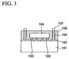
- the wafer level CSP has a structure shown in FIG.1, for example.
- wirings 102 are formed on a first semiconductor device chip 101, and a second semiconductor device chip 104 is secured to the wirings 102 via solder balls 103.
- the second semiconductor device chip 104 is smaller in size than the first semiconductor device chip 101.
- pin type terminals (vias) 105 are connected to the wirings 102 on the first semiconductor device chip 101 in the peripheral area of the second semiconductor device chip 104.
- a sealing resin 106 for sealing the second semiconductor device chip 104 is formed on an upper surface of the first semiconductor device chip 101 to have such a thickness that upper ends of the terminals 105 are exposed from the resin.
- a solder ball 107 is connected to the upper ends of the terminals 105 respectively.
- the terminals 105 shown in FIG.1 are formed on the wirings 102 by the plating method. Thus, it takes much time to form the terminals 105 and thus throughput of the CSP formation is gone down.
- forming areas of the terminals 105 are limited to the periphery of the second semiconductor device chip 104. Thus, it is not expected to increase the number of the terminals 105.
- a semiconductor device which comprises a first semiconductor chip having a first terminal on one surface; a second semiconductor chip which is larger than the first semiconductor chip and on which the first semiconductor chip is stacked, and which has a second terminal on one surface; an insulating layer formed on second semiconductor chip to cover the first semiconductor chip; a plurality of holes formed in the insulating layer; a conductive via formed like a film on inner peripheral surfaces and bottom surfaces of the holes and connected electrically to at least one of the first terminal and the second terminal; a first wiring pattern formed on an upper surface of the insulating layer; and an external terminal formed on the first wiring pattern.
- the insulating layer for covering the first semiconductor chip is formed on the second semiconductor chip, the holes are formed in the insulating layer, the film-like vias are formed in the hole respectively, and the wiring patterns are formed on the insulating layer.
- the vias can be formed in a short time, and both the wiring patterns and the vias can be formed by the same conductive film, and thus the number of the film forming steps can be reduced.
- the wiring patterns formed on the insulating layer are led onto the first semiconductor chip and then the external terminals are formed on the wiring patterns. Therefore, the narrower pitch between plural external terminals on the insulating layer can be suppressed, and also the number of the external terminals can be increased.
- corrosion of the vias can be prevented by covering the vias in the holes with the insulating layer.
- migration short and corrosion of the first wiring patterns can be prevented by covering the first wiring patterns except the portions to be connected to the wiring patterns on the insulating layer with another insulating layer.
- the wafer-level laminated package can be formed by the same technology independently of whether a circuit surface of the first semiconductor chip on which the first terminals are formed is face-up or face-down bonded on a circuit surface of the second semiconductor chip on which the first terminals are formed. Also, the face up bonding or the face down bonding can be used in its proper way, and also the semiconductor devices having various functions can be stacked. Therefore, the present invention is useful.
- the external terminals can be formed at any positions to correspond to a multi-pin structure.
- a plurality of semiconductor chips can be mounted by forming the above insulating layer having the wiring patterns and the vias therein as a multi-layered structure or by stacking the above mentioned structures.
- FIG.2 to FIG.5 are sectional views showing steps of forming a multi-chip package (MCP) according to a first embodiment of the present invention.
- MCP multi-chip package
- a semiconductor wafer 1 in which a first semiconductor circuit (not shown) is formed in a plurality of device areas A respectively is prepared.
- the semiconductor wafer 1 has a protection insulating layer 2 on its upper surface, as shown in a fragmental enlarged view of FIG.6A, and openings 2a to expose a first terminal (conductive pad) 3 that is connected electrically to an internal wiring (not shown) of the semiconductor device are formed in the protection insulating layer 2.
- the first terminal 3 is formed of aluminum, copper, or the like.
- the semiconductor wafer 1 is composed of a silicon wafer, for example, and is cut away in the later step every first semiconductor circuit and divided into the device area A unit.
- first rewiring patterns 4 are formed by forming a metal film having a double-layered structure made of titanium and nickel on the protection insulating layer 2 and the first terminals 3 to have a thickness of about 0.5 ⁇ m, and then patterning the metal film by means of the photolithography method.
- the first rewiring pattern 4 is a conductive pattern that is led from an upper surface of the first terminal 3 to an upper surface of the protection insulating layer 2.
- first semiconductor device chips 5 on which a second semiconductor circuit (not shown) is formed respectively are prepared.
- the first semiconductor device chip 5 is formed of a silicon chip, for example, which is smaller than the device area A of the semiconductor wafer 1, and has a protection insulating layer 6 on its upper surface. Openings 6a to expose second terminals 7 that are connected to wirings (not shown) in the first semiconductor device chip 5 are formed in the protection insulating layer 6. Also, second rewiring patterns 8 each of which is led from an upper surface of the second terminal 7 are formed on the protection insulating layer 6.
- each first semiconductor device chip 5 is bonded to a center portion of the device area A of the semiconductor wafer 1 via a die bonding agent (adhesive) 9.
- a resin insulating layer 10 made of epoxy, polyimide, or the like is formed on an upper surface of the semiconductor wafer 1 to have a thickness that is higher than the first semiconductor device chip 5 by about 10 to 20 ⁇ m.
- the first semiconductor device chips 5 are covered with the resin insulating layer 10.
- the resin insulating layer 10 is formed on the semiconductor wafer 1 by the spin coating, the printing, the laminating method, or the like.
- a countermeasure to prevent generation of the bubble in overlying areas of the first semiconductor device chips 5 and their peripheral areas must be taken by adjusting sufficiently a film thickness of the resin insulating layer 10, etc.
- the resin insulating layer 10 made of epoxy resin, polyimide, or the like, for example, is formed on the semiconductor wafer 1 to have a thickness of 120 to 150 ⁇ m, for example, and then the upper surface of the resin insulating layer 10 is planarized by the mechanical polishing method or the chemical-mechanical polishing method.
- via holes (through holes) 10a each having a diameter of 80 to 100 ⁇ m are formed in the resin insulating layer 10 on the first rewiring patterns 4 and the second rewiring patterns 8 respectively.
- the via holes 10a are formed easily by exposing the resin insulating layer 10 by using an exposure mask for the via hole formation and then developing the resin insulating layer 10 by using an inorganic alkaline solution such as sodium carbonate (NaCO 3 ), or the like after the resin insulating layer 10 is formed on the semiconductor wafer 1 in the non-exposure light environment.
- an inorganic alkaline solution such as sodium carbonate (NaCO 3 ), or the like after the resin insulating layer 10 is formed on the semiconductor wafer 1 in the non-exposure light environment.
- the via holes 10a should be formed by irradiating a high energy such as the laser, or the like onto predetermined positions of the resin insulating layer 10.
- a high energy such as the laser, or the like
- the via holes 10a are formed by the laser, it is not possible that the first terminals 3 made of the relatively soft conductive material such as aluminum, copper, or the like and the neighboring protection insulating layer 2 are removed or deteriorated by the laser irradiation because the first terminals 3 and the protection insulating layer 2 located under the via holes 10a are covered with the first rewiring pattern 4 made of a hard metal.
- the via holes 10a may be formed by the drilling.
- the surface of the resin insulating layer 10 is activated by the diluent solvent, and then a metal film 11, e.g., a copper film, of 0.5 to 1.0 ⁇ m thickness is formed on the upper surface of the resin insulating layer 10 and inner peripheral surfaces and bottom surfaces of the via holes 10a by the electroless plating.
- the metal film 11 having such thickness is formed in a very short time in contrast to the case where the external terminals 105 shown in FIG.1 are formed by the plating. In this case, the metal film 11 is connected to the upper surfaces of the first rewiring patterns 4 in the via holes 10a.
- the metal film may be formed herein to have a multi-layered structure.
- the metal film 11 when it is desired to form the metal film 11 of about 3 to 5 ⁇ m thickness, a method for forming the film thin once by virtue of the electroless plating method and then forming the film thick by virtue of the electroplating method may be employed. Also, in the case where the resin insulating layer 10 is formed of epoxy resin or polyimide, the growth of the metal film 11 on the upper surface of the resin insulating layer 10 and the inner surfaces of the via holes 10a by the electroless plating is easy.
- the metal film 11 is patterned by the photolithography method.
- the metal film 11 in the via holes 10a is left as vias 11a and also patterns of the metal film 11 on the upper surface of the resin insulating layer 10 are used as third rewiring patterns 11b.
- a plurality of third rewiring patterns 11b on the resin insulating layer 10 are connected electrically to the second terminals 7 of the first semiconductor device chips 5 via the holes 10a and the second rewiring patterns 8 respectively, and also connected electrically to the first terminals 3 of the semiconductor wafer 1 via the vias 11a and the first rewiring patterns 4.
- the second terminals 7 of the first semiconductor device chips 5 are connected electrically to the first terminals 3 of the semiconductor wafer 1 via the vias 11a and the third rewiring patterns 11b respectively.
- all the vias 11a are connected to the third rewiring patterns 11b respectively, but the vias 11a that are not connected to such pattern may be provided.
- buried insulating layers 12 are formed by filling the non-photosensitive epoxy resin into the opening portions 10a in the resin insulating layer 10 by using the squeegee or the printing method.
- the via 11a in the opening portion 10a is covered with the buried insulating layer 12.
- an insulating resin cover layer 13 made of a photosensitive epoxy resin, a photosensitive novolak resin, or the like is formed on the resin insulating layer 10, the third rewiring patterns 11b, and the buried insulating layers 12 respectively.
- the resin cover layer 13 is coated on the resin insulating layer 10 in the non-exposure light environment by using the squeegee or by the printing method.
- the resin cover layer 13 prevents corrosion of the third rewiring patterns 11b and prevents the migration short of the third rewiring patterns 11b.
- openings 13a for exposing contact portions of the third rewiring patterns 11b are patterned by exposing/developing the resin cover layer 13.
- external terminals 14 such as solder bumps, or the like are connected to the third rewiring patterns 11b through the openings 13a in the resin cover layer 13.
- the external terminals 14 are formed in the openings 13a in the resin cover layer 13, displacement is prevented or positioning is facilitated.
- a diameter of the opening 13a is expanded upward in a taper shape by the exposure and the development, the positioning and the connection of the ball-like external terminals 14 on the third rewiring patterns 11b are made easy.
- the semiconductor device is divided into a plurality of second semiconductor device chips 1a by dicing boundaries between the device areas A of the semiconductor wafer 1 shown in FIG.5B.
- a plurality of MCP semiconductor devices shown in FIG. 7 are formed.
- side surfaces of the second semiconductor device chip 1a are not covered with the resin insulating layer 10 to expose.
- a bottom surface of the semiconductor wafer 1 may be polished by the mechanical polishing method or the chemical-mechanical polishing method.
- the via holes 10a are formed around the first semiconductor device chips 5 in the resin insulating layer 10 formed on the upper surfaces of the second semiconductor device chips 1a, also the conductive films formed on the inner peripheral surfaces and the bottom surfaces of the via holes 10a are used as the vias 11a, and also the conductive films on the upper surface of the resin insulating layer 10 are used as the third rewiring patterns 11b.
- the formation of the vias 11a to be formed in the via holes 10a is executed by the step of forming the metal film 11.
- the vias can be formed in a short time rather than the conventional structure in which the via holes are buried completely.
- the portion of the metal film 11 constituting the via 11a, which is formed on the upper surface of the resin insulating layer 10, is patterned and used as the third rewiring pattern 11b.
- the external terminals 14 are formed over the first semiconductor device chips 5, so that the number of the external terminals 14 can be increased rather than the prior art and also a narrower pitch between the external terminals 14 can be relaxed.
- both the vias 11a and the third rewiring patterns 11b are formed by the same metal film 11, the throughput can be improved rather than the case they are formed separately respectively.
- the first semiconductor device chips 5 are adhered onto the semiconductor wafer 1, then the resin insulating layer 10, the vias 11a, the third rewiring patterns 11b, the resin cover layer 13, and the external terminals 14 are formed, and then the semiconductor wafer 1 is divided separately.
- first the semiconductor wafer 1 may be divided into a plurality of second semiconductor device chips 1a, then the first semiconductor device chips 5 may be adhered onto the second semiconductor device chips 1a respectively, and then the resin insulating layer 10, the vias 11a, the third rewiring patterns 11b, the resin cover layer 13, and the external terminals 14 may be formed.
- the semiconductor device having the same structure as shown in FIG.7 is also formed. In this case, the side surfaces of the second semiconductor device chip 1a are covered with the resin insulating layer 10.
- the wiring structure layers having the resin insulating layer 10, the vias 11a, and the third rewiring patterns 11b may be formed as a multi-layered wiring structure having two layers or more.
- the resin cover layer 13 and the external terminals 14 are formed on the uppermost resin insulating layer 10.
- upper and lower rewiring patterns 11b are arranged in such a manner that they intersect with each other to deal with the high-speed signal processing.
- Such multi-layered wiring structure may be employed in embodiments given in the following.
- the vias 11a and the third rewiring patterns 11b are formed, then the buried insulating layers 12 are formed in the via holes 10a, and then the resin cover layer 13 is formed on the resin insulating layer 10.
- the buried insulating layers 12 and the resin cover layer 13 may be formed at the same time.
- a photosensitive resin layer 15 e.g., an epoxy resin
- the epoxy resin in the via holes 10a is used as the buried insulating layers respectively, and the epoxy resin on the resin insulating layer 10 is used as the resin cover layer. Also, the buried insulating layers and the resin cover layer can be formed at the same time, whereby the number of the steps of forming the insulating layer can be reduced in contrast to the first embodiment.
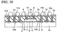
- a semiconductor device shown in FIG.10 is formed by cutting off the boundaries between the device areas A.
- the side surfaces of the second semiconductor device chip 1a are not covered with the resin insulating layer 10 and are exposed.
- a coating conductive layer 16 made of nickel-phosphorus (NiP), nickel, gold, or the like is formed selectively on the first terminals 3 in the openings 2a of the protection insulating layer 2 on the semiconductor wafer 1 by the electroless plating method to have a thickness of 3 to 5 ⁇ m.
- the first semiconductor device chips 5 are secured onto the semiconductor wafer 1 by the same method as the first embodiment.
- a chip having a structure in which not the second rewiring pattern but a coating conductive layer 17 made of NiP is formed on the second terminals 7 in the protection insulating layer 6 on the upper surface is employed.
- the resin insulating layer 10 is formed on the semiconductor wafer 1 to cover the first semiconductor device chip 5.
- the same methods as the first embodiment are employed to form and planarize the resin insulating layer 10.
- the via holes 10a are formed in the resin insulating layer 10 on the coating conductive layers 16, 17 on the first and second terminals 3, 7 on the semiconductor wafer 1 and the first semiconductor device chip 5 respectively.
- the via holes 10a are formed by the exposure and the development when the resin insulating layer 10 is formed of the photosensitive material, while the via holes 10a are formed by the laser irradiation when the resin insulating layer 10 is formed of the non-photosensitive material.
- the via holes 10a may be formed by the drilling.
- the vias 11a and the third rewiring patterns 11b are formed in the via holes 10a and on the resin insulating layer 10 via the steps similar to those in the first embodiment respectively.
- the buried insulating layers 12, the cover insulating layer 13, and the external terminals 14 are formed.
- the buried insulating layers 12 and the cover insulating layer 13 may be formed of the same resin layer 15 at the same time, as shown in the second embodiment.
- the semiconductor wafer 1 is divided into a plurality of second semiconductor device chips 1a every device area A.
- a semiconductor device shown in FIG.14 is formed.
- the side surfaces of the second semiconductor device chip 1a are not covered with the resin insulating layer 10 and exposed.
- the inorganic alkali used to form the via holes 10a in the resin insulating layer 10 can be prevented from being supplied to the terminals 3, 7 by the coating conductive layers 16, 17, or the laser used to form the via holes 10a can be prevented from being irradiated onto the terminals 3, 7 by the coating conductive layers 16, 17.
- the degradation of the first and second terminals 3, 7 can be prevented.
- the rewiring patterns may be formed on any one of the first semiconductor device chips 5 and the semiconductor wafer 1.
- the terminals 3, 7 that are not covered with the rewiring patterns must be covered with the coating conductive layers 16, 17.
- the first semiconductor device chips 5 shown in FIG.6B may be connected to the first terminals 3 on the semiconductor wafer 1 via not the third rewiring patterns 11b formed on the upper surface of the resin insulating layer 10 but the wires or the solder balls.
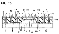
- such a structure may be employed that not the rewiring patterns but the coating conductive layers 17 made of nickel-phosphorus are formed on the second terminal 7 of the first semiconductor device chip 5 and then the coating conductive layers 17 and the first rewiring patterns 4 on the semiconductor wafer 1 (the second semiconductor device chip 1a) are connected via gold (conductive) wires 21 by the wire bonding.
- no via hole 10a is formed in the resin insulating layer 10 on the first semiconductor device chip 5.
- solder bumps (external terminals) 22 may be connected onto the second terminal 7 of the first semiconductor device chip 5, and then the solder bumps 22 may be connected onto the first rewiring patterns 4 on the semiconductor wafer 1 (the second semiconductor device chip 1a). In this case, no via hole 10a is also formed in the resin insulating layer 10 on the first semiconductor device chip 5.
- the via holes 10a are not formed in the resin insulating layer 10 shown in FIG.15, FIG.16 over the first semiconductor device chips 5, but the third rewiring patterns 11b are formed on the resin insulating layer 10 and then the external terminals 14 are bonded thereon.
- the forming areas of the external terminals 14 on the resin insulating layer 10 can be widened rather than the prior art, and the number of the external terminals 14 can be increased rather than the prior art, and also the narrower pitch between the external terminals 14 can be relaxed.
- the insulating layer for covering the first semiconductor chip is formed on the second semiconductor chip, the holes are formed in the insulating layer, the film-like vias are formed in the hole respectively, and the wiring patterns are formed on the insulating layer. Therefore, the vias can be formed in a short time, and both the wiring patterns and the vias can be formed by the same conductive film, and thus the number of the film forming steps can be reduced.
- the wiring patterns on the insulating layer are led onto the first semiconductor chip and then the external terminals are formed on the wiring patterns. Therefore, the narrower pitch between plural external terminals on the insulating layer can be suppressed, and also the number of the external terminals can be increased.
- corrosion of the vias can be prevented by covering the vias in the holes with the insulating layer, and also migration short and corrosion of the first wiring patterns can be prevented by covering the first wiring patterns on the insulating layer except the portions to be connected to the external terminals with another insulating layer.
Landscapes
- Internal Circuitry In Semiconductor Integrated Circuit Devices (AREA)
Abstract
Description
Claims (20)
- A semiconductor device comprising:a first semiconductor chip having a first terminal on one surface;a second semiconductor chip which is larger than the first semiconductor chip and on which the first semiconductor chip is stacked, and which has a second terminal on one surface;an insulating layer formed on second semiconductor chip to cover the first semiconductor chip;a plurality of holes formed in the insulating layer;a conductive via formed like a film on inner peripheral surfaces and bottom surfaces of the holes and connected electrically to at least one of the first terminal and the second terminal;a first wiring pattern formed on an upper surface of the insulating layer; andan external terminal formed on the first wiring pattern.
- A semiconductor device according to claim 1, wherein the first semiconductor chip is mounted on the second semiconductor chip to direct the first terminal and the second terminal in a same direction.
- A semiconductor device according to claim 2, wherein the first terminal of the first semiconductor chip is connected to the second terminal of the second semiconductor chip via a conductive wire.
- A semiconductor device according to claim 2, wherein the first terminal of the first semiconductor chip is connected electrically to the second terminal of the second semiconductor chip via the first wiring pattern and the via.
- A semiconductor device according to claim 2, wherein the first semiconductor chip is mounted on the second semiconductor chip via an adhesive.
- A semiconductor device according to claim 1, wherein the first semiconductor chip and the second semiconductor chip are stacked so as to oppose surfaces having the first terminal and the second terminal to each other.
- A semiconductor device according to claim 6, wherein a third wiring pattern connected electrically to the second terminal is formed on the second semiconductor chip, and the first terminal of the first semiconductor chip is connected to the third wiring pattern via conductive material.
- A semiconductor device according to claim 1, wherein a second wiring pattern is formed on at least one of the first terminal and the second terminal, and the via is formed on the second wiring pattern.
- A semiconductor device according to claim 1, wherein at least one of the first terminal and the second terminal is connected to the via via a coating conductive layer.
- A semiconductor device according to claim 1, wherein the via and the first wiring pattern are connected mutually.
- A semiconductor device according to claim 1, wherein the via is buried in an insulating layer in the holes.
- A semiconductor device according to claim 1, wherein the first wiring pattern except a portion connected to the external terminal is covered with a cover insulating layer on the insulating layer.
- A semiconductor device according to claim 1, wherein a surface of the via and an area of the first wiring pattern except the portion connected to the external terminal in the holes are covered with a same insulating layer.
- A semiconductor device according to claim 1, wherein side surfaces of the second semiconductor chip are exposed.
- A method for manufacturing a semiconductor device comprising the steps of:adhering a first semiconductor chip having a first terminal to a semiconductor substrate which is larger than the first semiconductor chip and has a second terminal;forming an insulating layer that covers the first semiconductor chip on the semiconductor substrate;forming a hole in the insulating layer;forming a conductive film in the hole and on the insulating layer;patterning the conductive film to leave as a via in the hole and form a wiring on the insulating layer; andconnecting an external terminal onto the wiring.
- A method for manufacturing a semiconductor device according to claim 15, wherein a metal pattern is formed on at least one of the first terminal and the second terminal, and the hole is formed on the metal pattern.
- A method for manufacturing a semiconductor device according to claim 16, wherein the metal pattern is a wiring pattern.
- A method for manufacturing a semiconductor device according to claim 15, wherein the hole is formed by any of a laser irradiation method, a photolithography method, and a drilling method.
- A method for manufacturing a semiconductor device according to claim 15, wherein the conductive film is a metal film formed by a plating method.
- A method for manufacturing a semiconductor device according to claim 15, wherein the insulating layer is formed of an epoxy resin or a polyimide resin.
Applications Claiming Priority (1)
| Application Number | Priority Date | Filing Date | Title |
|---|---|---|---|
| PCT/JP2001/010722 WO2003049184A1 (en) | 2001-12-07 | 2001-12-07 | Semiconductor device and method for manufacturing the same |
Publications (2)
| Publication Number | Publication Date |
|---|---|
| EP1455392A1 true EP1455392A1 (en) | 2004-09-08 |
| EP1455392A4 EP1455392A4 (en) | 2008-05-07 |
Family
ID=11738006
Family Applications (1)
| Application Number | Title | Priority Date | Filing Date |
|---|---|---|---|
| EP01274912A Ceased EP1455392A4 (en) | 2001-12-07 | 2001-12-07 | SEMICONDUCTOR DEVICE AND METHOD FOR MANUFACTURING THE SAME |
Country Status (6)
| Country | Link |
|---|---|
| US (2) | US7084513B2 (en) |
| EP (1) | EP1455392A4 (en) |
| JP (1) | JP4182189B2 (en) |
| KR (1) | KR100636259B1 (en) |
| CN (1) | CN100350607C (en) |
| WO (1) | WO2003049184A1 (en) |
Cited By (5)
| Publication number | Priority date | Publication date | Assignee | Title |
|---|---|---|---|---|
| DE102004048203A1 (en) * | 2004-09-30 | 2005-12-29 | Infineon Technologies Ag | Stackable semiconductor module for electronics packaging has electronic component with vertical opening provided with continuous metallization with layer of soldering paste to connect it to contact of another electronic component |
| WO2008049672A1 (en) * | 2006-10-25 | 2008-05-02 | Robert Bosch Gmbh | Electrical component comprising contact means |
| US9446943B2 (en) | 2013-05-31 | 2016-09-20 | Stmicroelectronics S.R.L. | Wafer-level packaging of integrated devices, and manufacturing method thereof |
| EP3163614A3 (en) * | 2015-10-05 | 2017-07-12 | MediaTek Inc. | Stacked fan-out package structure |
| US9802813B2 (en) | 2014-12-24 | 2017-10-31 | Stmicroelectronics (Malta) Ltd | Wafer level package for a MEMS sensor device and corresponding manufacturing process |
Families Citing this family (76)
| Publication number | Priority date | Publication date | Assignee | Title |
|---|---|---|---|---|
| US6710454B1 (en) | 2000-02-16 | 2004-03-23 | Micron Technology, Inc. | Adhesive layer for an electronic apparatus having multiple semiconductor devices |
| CN100350607C (en) * | 2001-12-07 | 2007-11-21 | 富士通株式会社 | Semiconductor device and manufacturing method thereof |
| US7548430B1 (en) | 2002-05-01 | 2009-06-16 | Amkor Technology, Inc. | Buildup dielectric and metallization process and semiconductor package |
| US9691635B1 (en) | 2002-05-01 | 2017-06-27 | Amkor Technology, Inc. | Buildup dielectric layer having metallization pattern semiconductor package fabrication method |
| US7633765B1 (en) * | 2004-03-23 | 2009-12-15 | Amkor Technology, Inc. | Semiconductor package including a top-surface metal layer for implementing circuit features |
| KR100574947B1 (en) * | 2003-08-20 | 2006-05-02 | 삼성전자주식회사 | BA package, manufacturing method thereof and BA package laminated structure |
| JP4271590B2 (en) * | 2004-01-20 | 2009-06-03 | 新光電気工業株式会社 | Semiconductor device and manufacturing method thereof |
| US11081370B2 (en) | 2004-03-23 | 2021-08-03 | Amkor Technology Singapore Holding Pte. Ltd. | Methods of manufacturing an encapsulated semiconductor device |
| US10811277B2 (en) | 2004-03-23 | 2020-10-20 | Amkor Technology, Inc. | Encapsulated semiconductor package |
| TWI250596B (en) | 2004-07-23 | 2006-03-01 | Ind Tech Res Inst | Wafer-level chip scale packaging method |
| CA2594483C (en) * | 2005-01-28 | 2014-08-26 | Duke University | Apparatuses and methods for manipulating droplets on a printed circuit board |
| US20060237828A1 (en) * | 2005-04-22 | 2006-10-26 | Robinson William D | System and method for enhancing wafer chip scale packages |
| US9601474B2 (en) | 2005-07-22 | 2017-03-21 | Invensas Corporation | Electrically stackable semiconductor wafer and chip packages |
| JP4395775B2 (en) * | 2005-10-05 | 2010-01-13 | ソニー株式会社 | Semiconductor device and manufacturing method thereof |
| TWI284976B (en) * | 2005-11-14 | 2007-08-01 | Via Tech Inc | Package, package module and manufacturing method of the package |
| JP2007207921A (en) * | 2006-01-31 | 2007-08-16 | Stanley Electric Co Ltd | Manufacturing method of surface mount type optical semiconductor device |
| US7884464B2 (en) * | 2006-06-27 | 2011-02-08 | Advanced Chip Engineering Technologies Inc. | 3D electronic packaging structure having a conductive support substrate |
| WO2008014633A1 (en) | 2006-06-29 | 2008-02-07 | Intel Corporation | Apparatus, system, and method for wireless connection in integrated circuit packages |
| KR100800476B1 (en) * | 2006-07-11 | 2008-02-04 | 삼성전자주식회사 | Semiconductor package and manufacturing method thereof and semiconductor module and manufacturing method thereof |
| TWI302732B (en) * | 2006-08-03 | 2008-11-01 | Unimicron Technology Corp | Embedded chip package process and circuit board with embedded chip |
| TWI335658B (en) * | 2006-08-22 | 2011-01-01 | Advanced Semiconductor Eng | Stacked structure of chips and wafer structure for making same |
| US7550857B1 (en) | 2006-11-16 | 2009-06-23 | Amkor Technology, Inc. | Stacked redistribution layer (RDL) die assembly package |
| US8178982B2 (en) * | 2006-12-30 | 2012-05-15 | Stats Chippac Ltd. | Dual molded multi-chip package system |
| US8304923B2 (en) * | 2007-03-29 | 2012-11-06 | ADL Engineering Inc. | Chip packaging structure |
| KR100871380B1 (en) | 2007-06-18 | 2008-12-02 | 주식회사 하이닉스반도체 | Semiconductor Package with Passive Device |
| JP5215605B2 (en) * | 2007-07-17 | 2013-06-19 | ラピスセミコンダクタ株式会社 | Manufacturing method of semiconductor device |
| US8293587B2 (en) | 2007-10-11 | 2012-10-23 | International Business Machines Corporation | Multilayer pillar for reduced stress interconnect and method of making same |
| KR20090055316A (en) * | 2007-11-28 | 2009-06-02 | 삼성전자주식회사 | Semiconductor package, method for manufacturing electronic device and semiconductor package having same |
| US8847377B2 (en) | 2008-01-02 | 2014-09-30 | SK Hynix Inc. | Stacked wafer level package having a reduced size |
| KR100910233B1 (en) * | 2008-01-02 | 2009-07-31 | 주식회사 하이닉스반도체 | Stacked Wafer Level Packages |
| CN101946409B (en) | 2008-02-18 | 2014-08-20 | 株式会社村田制作所 | Elastic wave device and manufacturing method thereof |
| US8637341B2 (en) * | 2008-03-12 | 2014-01-28 | Infineon Technologies Ag | Semiconductor module |
| US8362617B2 (en) * | 2008-05-01 | 2013-01-29 | Infineon Technologies Ag | Semiconductor device |
| US7888184B2 (en) * | 2008-06-20 | 2011-02-15 | Stats Chippac Ltd. | Integrated circuit packaging system with embedded circuitry and post, and method of manufacture thereof |
| US8354304B2 (en) * | 2008-12-05 | 2013-01-15 | Stats Chippac, Ltd. | Semiconductor device and method of forming conductive posts embedded in photosensitive encapsulant |
| US20100148337A1 (en) * | 2008-12-17 | 2010-06-17 | Yong Liu | Stackable semiconductor package and process to manufacture same |
| US8003445B2 (en) * | 2009-03-26 | 2011-08-23 | Stats Chippac Ltd. | Integrated circuit packaging system with z-interconnects having traces and method of manufacture thereof |
| JP5165006B2 (en) * | 2010-01-25 | 2013-03-21 | 株式会社テラミクロス | Manufacturing method of semiconductor device |
| US8138014B2 (en) | 2010-01-29 | 2012-03-20 | Stats Chippac, Ltd. | Method of forming thin profile WLCSP with vertical interconnect over package footprint |
| US8455300B2 (en) | 2010-05-25 | 2013-06-04 | Stats Chippac Ltd. | Integrated circuit package system with embedded die superstructure and method of manufacture thereof |
| US8343810B2 (en) | 2010-08-16 | 2013-01-01 | Stats Chippac, Ltd. | Semiconductor device and method of forming Fo-WLCSP having conductive layers and conductive vias separated by polymer layers |
| JP5703010B2 (en) | 2010-12-16 | 2015-04-15 | 新光電気工業株式会社 | Semiconductor package and manufacturing method thereof |
| US8765525B2 (en) | 2011-06-16 | 2014-07-01 | Stats Chippac Ltd. | Method of manufacturing an integrated circuit packaging system including lasering through encapsulant over interposer |
| TWI469292B (en) * | 2011-07-26 | 2015-01-11 | 萬國半導體股份有限公司 | Stacked power semiconductor device using dual lead frame and manufacturing method |
| US8487421B2 (en) * | 2011-08-01 | 2013-07-16 | Tessera, Inc. | Microelectronic package with stacked microelectronic elements and method for manufacture thereof |
| US20130040423A1 (en) | 2011-08-10 | 2013-02-14 | Taiwan Semiconductor Manufacturing Company, Ltd. | Method of Multi-Chip Wafer Level Packaging |
| CN103383927A (en) * | 2012-05-03 | 2013-11-06 | 三星电子株式会社 | Semiconductor encapsulation and forming method thereof |
| US8901730B2 (en) | 2012-05-03 | 2014-12-02 | Taiwan Semiconductor Manufacturing Company, Ltd. | Methods and apparatus for package on package devices |
| TWI562295B (en) | 2012-07-31 | 2016-12-11 | Mediatek Inc | Semiconductor package and method for fabricating base for semiconductor package |
| US9177899B2 (en) | 2012-07-31 | 2015-11-03 | Mediatek Inc. | Semiconductor package and method for fabricating base for semiconductor package |
| US10991669B2 (en) | 2012-07-31 | 2021-04-27 | Mediatek Inc. | Semiconductor package using flip-chip technology |
| US9953907B2 (en) | 2013-01-29 | 2018-04-24 | Taiwan Semiconductor Manufacturing Company, Ltd. | PoP device |
| US8778738B1 (en) | 2013-02-19 | 2014-07-15 | Taiwan Semiconductor Manufacturing Company, Ltd. | Packaged semiconductor devices and packaging devices and methods |
| US8970023B2 (en) * | 2013-02-04 | 2015-03-03 | Taiwan Semiconductor Manufacturing Company, Ltd. | Package structure and methods of forming same |
| KR101488590B1 (en) | 2013-03-29 | 2015-01-30 | 앰코 테크놀로지 코리아 주식회사 | Semiconductor device and manufacturing method thereof |
| US9653442B2 (en) * | 2014-01-17 | 2017-05-16 | Taiwan Semiconductor Manufacturing Company, Ltd. | Integrated circuit package and methods of forming same |
| US9704841B2 (en) | 2014-03-26 | 2017-07-11 | United Microelectronics Corp. | Method of packaging stacked dies on wafer using flip-chip bonding |
| KR102161776B1 (en) | 2014-03-28 | 2020-10-06 | 에스케이하이닉스 주식회사 | Stack package |
| US9330994B2 (en) | 2014-03-28 | 2016-05-03 | Stats Chippac, Ltd. | Semiconductor device and method of forming RDL and vertical interconnect by laser direct structuring |
| JP6317629B2 (en) * | 2014-06-02 | 2018-04-25 | 株式会社東芝 | Semiconductor device |
| US11239138B2 (en) | 2014-06-27 | 2022-02-01 | Taiwan Semiconductor Manufacturing Company | Methods of packaging semiconductor devices and packaged semiconductor devices |
| US10177115B2 (en) * | 2014-09-05 | 2019-01-08 | Taiwan Semiconductor Manufacturing Company, Ltd. | Package structures and methods of forming |
| KR102352237B1 (en) | 2014-10-23 | 2022-01-18 | 삼성전자주식회사 | method for fabricating fan-out wafer level package and the structure of the same |
| US9627311B2 (en) | 2015-01-22 | 2017-04-18 | Mediatek Inc. | Chip package, package substrate and manufacturing method thereof |
| KR102505189B1 (en) * | 2015-07-22 | 2023-03-02 | 인텔 코포레이션 | multi-layer package |
| US11037904B2 (en) * | 2015-11-24 | 2021-06-15 | Taiwan Semiconductor Manufacturing Company, Ltd. | Singulation and bonding methods and structures formed thereby |
| KR101803929B1 (en) | 2016-03-10 | 2018-01-11 | 주식회사 소프트에피 | Light emitting device emiting near-uv rays and iii-nitride semiconductor template used for the smae |
| US10068853B2 (en) * | 2016-05-05 | 2018-09-04 | Taiwan Semiconductor Manufacturing Co., Ltd. | Integrated fan-out package and method of fabricating the same |
| US10177078B2 (en) * | 2016-11-28 | 2019-01-08 | Taiwan Semiconductor Manufacturing Co., Ltd. | Method for forming chip package structure |
| US10510722B2 (en) * | 2017-06-20 | 2019-12-17 | Taiwan Semiconductor Manufacturing Company Ltd. | Semiconductor device and method for manufacturing the same |
| US10879220B2 (en) * | 2018-06-15 | 2020-12-29 | Taiwan Semiconductor Manufacturing Company, Ltd. | Package-on-package structure and manufacturing method thereof |
| CN110875294B (en) * | 2018-08-29 | 2024-01-23 | 恒劲科技股份有限公司 | Package structure of semiconductor device and manufacturing method thereof |
| CN111341750B (en) * | 2018-12-19 | 2024-03-01 | 奥特斯奥地利科技与系统技术有限公司 | Component carrier including conductive base structure and method of manufacturing |
| US11387177B2 (en) * | 2019-06-17 | 2022-07-12 | Taiwan Semiconductor Manufacturing Company Ltd. | Package structure and method for forming the same |
| US11063019B2 (en) * | 2019-07-17 | 2021-07-13 | Taiwan Semiconductor Manufacturing Company, Ltd. | Package structure, chip structure and method of fabricating the same |
| US11735554B2 (en) * | 2020-08-14 | 2023-08-22 | Sj Semiconductor (Jiangyin) Corporation | Wafer-level chip scale packaging structure having a rewiring layer and method for manufacturing the wafer-level chip scale packaging structure |
Family Cites Families (27)
| Publication number | Priority date | Publication date | Assignee | Title |
|---|---|---|---|---|
| JP2593965B2 (en) * | 1991-01-29 | 1997-03-26 | 三菱電機株式会社 | Semiconductor device |
| JP3397542B2 (en) * | 1994-10-03 | 2003-04-14 | 株式会社東芝 | Semiconductor package integrated with semiconductor chip and method of manufacturing the same |
| EP0706208B1 (en) * | 1994-10-03 | 2002-06-12 | Kabushiki Kaisha Toshiba | Method of manufacturing of a semiconductor package integral with semiconductor chip. |
| US5886412A (en) * | 1995-08-16 | 1999-03-23 | Micron Technology, Inc. | Angularly offset and recessed stacked die multichip device |
| JP3644662B2 (en) * | 1997-10-29 | 2005-05-11 | 株式会社ルネサステクノロジ | Semiconductor module |
| US6025995A (en) * | 1997-11-05 | 2000-02-15 | Ericsson Inc. | Integrated circuit module and method |
| JP3481444B2 (en) * | 1998-01-14 | 2003-12-22 | シャープ株式会社 | Semiconductor device and manufacturing method thereof |
| JP3512657B2 (en) * | 1998-12-22 | 2004-03-31 | シャープ株式会社 | Semiconductor device |
| JP2000223645A (en) * | 1999-02-01 | 2000-08-11 | Mitsubishi Electric Corp | Semiconductor device |
| US6291884B1 (en) * | 1999-11-09 | 2001-09-18 | Amkor Technology, Inc. | Chip-size semiconductor packages |
| KR100347135B1 (en) * | 1999-12-24 | 2002-07-31 | 주식회사 하이닉스반도체 | Wafer level multi-chip package and the manufacturing method |
| US6348728B1 (en) | 2000-01-28 | 2002-02-19 | Fujitsu Limited | Semiconductor device having a plurality of semiconductor elements interconnected by a redistribution layer |
| JP3996315B2 (en) * | 2000-02-21 | 2007-10-24 | 松下電器産業株式会社 | Semiconductor device and manufacturing method thereof |
| JP3651346B2 (en) * | 2000-03-06 | 2005-05-25 | カシオ計算機株式会社 | Semiconductor device and manufacturing method thereof |
| JP3772066B2 (en) * | 2000-03-09 | 2006-05-10 | 沖電気工業株式会社 | Semiconductor device |
| KR100559664B1 (en) * | 2000-03-25 | 2006-03-10 | 앰코 테크놀로지 코리아 주식회사 | Semiconductor Package |
| JP4178715B2 (en) * | 2000-04-14 | 2008-11-12 | 松下電器産業株式会社 | Semiconductor device and manufacturing method thereof |
| JP2002009236A (en) * | 2000-06-21 | 2002-01-11 | Shinko Electric Ind Co Ltd | Multilayer semiconductor device and method of manufacturing the same |
| US6452278B1 (en) * | 2000-06-30 | 2002-09-17 | Amkor Technology, Inc. | Low profile package for plural semiconductor dies |
| JP2002043503A (en) * | 2000-07-25 | 2002-02-08 | Nec Kyushu Ltd | Semiconductor device |
| JP2002050721A (en) * | 2000-08-03 | 2002-02-15 | Hitachi Cable Ltd | Electronic device and method of manufacturing the same |
| TW454287B (en) * | 2000-12-06 | 2001-09-11 | Siliconware Precision Industries Co Ltd | Multi-media chip package and its manufacture |
| TW502408B (en) * | 2001-03-09 | 2002-09-11 | Advanced Semiconductor Eng | Chip with chamfer |
| US6734568B2 (en) * | 2001-08-29 | 2004-05-11 | Kabushiki Kaisha Toshiba | Semiconductor device and method of manufacturing the same |
| TW550997B (en) * | 2001-10-18 | 2003-09-01 | Matsushita Electric Industrial Co Ltd | Module with built-in components and the manufacturing method thereof |
| CN100350607C (en) * | 2001-12-07 | 2007-11-21 | 富士通株式会社 | Semiconductor device and manufacturing method thereof |
| JP3904541B2 (en) * | 2003-09-26 | 2007-04-11 | 沖電気工業株式会社 | Manufacturing method of semiconductor device embedded substrate |
-
2001
- 2001-12-07 CN CNB018238653A patent/CN100350607C/en not_active Expired - Fee Related
- 2001-12-07 JP JP2003550280A patent/JP4182189B2/en not_active Expired - Fee Related
- 2001-12-07 WO PCT/JP2001/010722 patent/WO2003049184A1/en not_active Ceased
- 2001-12-07 KR KR1020047008710A patent/KR100636259B1/en not_active Expired - Fee Related
- 2001-12-07 EP EP01274912A patent/EP1455392A4/en not_active Ceased
-
2004
- 2004-06-04 US US10/860,657 patent/US7084513B2/en not_active Expired - Fee Related
-
2006
- 2006-06-30 US US11/477,550 patent/US7759246B2/en not_active Expired - Fee Related
Cited By (7)
| Publication number | Priority date | Publication date | Assignee | Title |
|---|---|---|---|---|
| DE102004048203A1 (en) * | 2004-09-30 | 2005-12-29 | Infineon Technologies Ag | Stackable semiconductor module for electronics packaging has electronic component with vertical opening provided with continuous metallization with layer of soldering paste to connect it to contact of another electronic component |
| WO2008049672A1 (en) * | 2006-10-25 | 2008-05-02 | Robert Bosch Gmbh | Electrical component comprising contact means |
| US9446943B2 (en) | 2013-05-31 | 2016-09-20 | Stmicroelectronics S.R.L. | Wafer-level packaging of integrated devices, and manufacturing method thereof |
| US9802813B2 (en) | 2014-12-24 | 2017-10-31 | Stmicroelectronics (Malta) Ltd | Wafer level package for a MEMS sensor device and corresponding manufacturing process |
| US10435290B2 (en) | 2014-12-24 | 2019-10-08 | Stmicroelectronics (Malta) Ltd | Wafer level package for a MEMS sensor device and corresponding manufacturing process |
| EP3163614A3 (en) * | 2015-10-05 | 2017-07-12 | MediaTek Inc. | Stacked fan-out package structure |
| US10692789B2 (en) | 2015-10-05 | 2020-06-23 | Mediatek Inc. | Stacked fan-out package structure |
Also Published As
| Publication number | Publication date |
|---|---|
| US7759246B2 (en) | 2010-07-20 |
| US20060246623A1 (en) | 2006-11-02 |
| JP4182189B2 (en) | 2008-11-19 |
| JPWO2003049184A1 (en) | 2005-04-21 |
| US20050001329A1 (en) | 2005-01-06 |
| KR100636259B1 (en) | 2006-10-19 |
| WO2003049184A1 (en) | 2003-06-12 |
| KR20040071177A (en) | 2004-08-11 |
| EP1455392A4 (en) | 2008-05-07 |
| US7084513B2 (en) | 2006-08-01 |
| CN1579020A (en) | 2005-02-09 |
| CN100350607C (en) | 2007-11-21 |
Similar Documents
| Publication | Publication Date | Title |
|---|---|---|
| US7759246B2 (en) | Semiconductor device having a plurality of semiconductor chips and method for manufacturing the same | |
| US12388046B2 (en) | Semiconductor package | |
| US7057290B2 (en) | Electronic parts packaging structure and method of manufacturing the same | |
| US7053475B2 (en) | Semiconductor device and manufacturing method therefor | |
| JP3813402B2 (en) | Manufacturing method of semiconductor device | |
| US7105423B2 (en) | Method of manufacturing semiconductor device | |
| US20020173133A1 (en) | Method for packaging a microelectronic device using on-die bond pad expansion | |
| KR102749213B1 (en) | Semiconductor package and method of manufacturing thereof | |
| US12381163B2 (en) | Semiconductor package and manufacturing method thereof | |
| KR100449307B1 (en) | Semiconductor device and method for manufacturing the same | |
| CN110556354B (en) | Package substrate and manufacturing method thereof | |
| CN113053759A (en) | Method for manufacturing semiconductor device | |
| KR20230134086A (en) | Heat dissipating features for laser drilling process | |
| KR20240007848A (en) | Semiconductor package and fabricating method thereof | |
| JP2004146728A (en) | Semiconductor device and its manufacturing method | |
| KR20250027433A (en) | Semiconductor package | |
| KR100596797B1 (en) | Manufacturing Method of Wafer Level Package | |
| KR20250043656A (en) | Semiconductor package | |
| CN120854291A (en) | Package and method of forming the same | |
| TW527708B (en) | Semiconductor device and method of manufacturing the same | |
| CN118198009A (en) | Semiconductor packaging |
Legal Events
| Date | Code | Title | Description |
|---|---|---|---|
| PUAI | Public reference made under article 153(3) epc to a published international application that has entered the european phase |
Free format text: ORIGINAL CODE: 0009012 |
|
| 17P | Request for examination filed |
Effective date: 20040630 |
|
| AK | Designated contracting states |
Kind code of ref document: A1 Designated state(s): DE FR GB |
|
| A4 | Supplementary search report drawn up and despatched |
Effective date: 20080409 |
|
| RIC1 | Information provided on ipc code assigned before grant |
Ipc: H01L 25/065 20060101AFI20080403BHEP Ipc: H01L 23/12 20060101ALI20080403BHEP Ipc: H01L 21/60 20060101ALI20080403BHEP |
|
| RAP1 | Party data changed (applicant data changed or rights of an application transferred) |
Owner name: FUJITSU MICROELECTRONICS LIMITED |
|
| RAP1 | Party data changed (applicant data changed or rights of an application transferred) |
Owner name: FUJITSU SEMICONDUCTOR LIMITED |
|
| 17Q | First examination report despatched |
Effective date: 20110120 |
|
| RAP1 | Party data changed (applicant data changed or rights of an application transferred) |
Owner name: SOCIONEXT INC. |
|
| REG | Reference to a national code |
Ref country code: DE Ref legal event code: R003 |
|
| STAA | Information on the status of an ep patent application or granted ep patent |
Free format text: STATUS: THE APPLICATION HAS BEEN REFUSED |
|
| 18R | Application refused |
Effective date: 20160206 |