EP1455378A1 - Sample imaging method and charged particle beam system - Google Patents
Sample imaging method and charged particle beam system Download PDFInfo
- Publication number
- EP1455378A1 EP1455378A1 EP20010274171 EP01274171A EP1455378A1 EP 1455378 A1 EP1455378 A1 EP 1455378A1 EP 20010274171 EP20010274171 EP 20010274171 EP 01274171 A EP01274171 A EP 01274171A EP 1455378 A1 EP1455378 A1 EP 1455378A1
- Authority
- EP
- European Patent Office
- Prior art keywords
- image
- charged particle
- sample
- particle beam
- images
- Prior art date
- Legal status (The legal status is an assumption and is not a legal conclusion. Google has not performed a legal analysis and makes no representation as to the accuracy of the status listed.)
- Granted
Links
Images






Classifications
-
- G—PHYSICS
- G01—MEASURING; TESTING
- G01N—INVESTIGATING OR ANALYSING MATERIALS BY DETERMINING THEIR CHEMICAL OR PHYSICAL PROPERTIES
- G01N23/00—Investigating or analysing materials by the use of wave or particle radiation, e.g. X-rays or neutrons, not covered by groups G01N3/00 – G01N17/00, G01N21/00 or G01N22/00
- G01N23/22—Investigating or analysing materials by the use of wave or particle radiation, e.g. X-rays or neutrons, not covered by groups G01N3/00 – G01N17/00, G01N21/00 or G01N22/00 by measuring secondary emission from the material
-
- H—ELECTRICITY
- H01—ELECTRIC ELEMENTS
- H01J—ELECTRIC DISCHARGE TUBES OR DISCHARGE LAMPS
- H01J37/00—Discharge tubes with provision for introducing objects or material to be exposed to the discharge, e.g. for the purpose of examination or processing thereof
- H01J37/02—Details
- H01J37/22—Optical, image processing or photographic arrangements associated with the tube
- H01J37/222—Image processing arrangements associated with the tube
-
- H—ELECTRICITY
- H01—ELECTRIC ELEMENTS
- H01J—ELECTRIC DISCHARGE TUBES OR DISCHARGE LAMPS
- H01J37/00—Discharge tubes with provision for introducing objects or material to be exposed to the discharge, e.g. for the purpose of examination or processing thereof
- H01J37/26—Electron or ion microscopes; Electron or ion diffraction tubes
- H01J37/28—Electron or ion microscopes; Electron or ion diffraction tubes with scanning beams
Definitions
- the present invention relates to a method of forming a sample image and a charged particle beam apparatus, and particularly to a method of forming a sample image and a charged particle beam apparatus which are suitable for obtaining a high resolution image in a high magnification and not influenced by image drift.
- a charged particle beam apparatus typical of which is a scanning electron microscope
- desired information for example, a sample image
- the resolution becomes higher year by year, and the required observation magnification becomes higher as the resolution becomes higher.
- the beam scanning method for obtaining a sample image there are a method which obtains a final objective image by adding a plurality of images obtained by high speed scanning and a method which obtains a final objective image by once of low speed scanning (acquiring time of one frame image: approximately 40 seconds to 80 seconds). The influence of the drift of a view area on the acquired image becomes more serious as the observation magnification becomes higher.
- the objective image after adding has blurs in a direction of the drift because displaced pixels of the view area are added. Reducing the influence of the drift may be attained by reducing number of adding frames and shortening the adding time, but this method can not obtain a sufficient S/N ratio.
- a technology is disclosed in Japanese Patent Application Laid-Open No.62-43050.
- the technology is that a pattern for detecting drift is stored, and a beam irradiating position is corrected by periodically acquiring an image of the pattern to detect a displacement between the acquired image and the stored pattern.
- a technology is disclosed in Japanese Patent Application Laid-Open No.5-290787.
- the technology is that two images are acquired based on electron beam scanning on a specified observed area, and pattern matching is performed in order to specify an amount of displacement and a direction of displacement between the both images, and pixels are added by moving the pixels by the specified amount of displacement and the specified direction of displacement.
- the accuracy of controlling the beam irradiating position becomes insufficient when the observation magnification becomes several hundred thousand times.
- the size of one pixel on the observation view area (on the sample) is approximately 0.5 nm.
- Measurement and evaluation with a higher magnification become necessary as the scale-down of a measured object is progressed.
- image shift drift below several nm causes "blurs" in a flame added image.
- an S/N ratio of image data before processing image adding is low and accordingly the displacement between the images is difficult to be detected, it is difficult to correct the displacement with high accuracy. Further, it can be considered that the S/N ratio is improved by increasing the probe current (the electron beam current) to increase the amount of secondary electron emission.
- the probe current the electron beam current
- the displacement between the images acquired at different timing is further increased by movement of the view area of the electron beam due to charging, and as the result, it has been difficult to correct the displacement with high accuracy.
- a sample weak against electron beam damage is irradiated by an electron beam having a large beam current, there is a problem in that the sample may be broken or evaporated.
- An object of the present invention is to provide a sample image forming method and a charged particle beam apparatus which are suitable for realizing suppressing of the view area displacement with high accuracy while the influence of charging due to irradiation of the charged particle beam is being suppressed.
- the present invention provide a method of forming a sample image by scanning a charged particle beam on a sample and forming an image based on secondary signals emitted from the sample, the method comprising the steps of forming a plurality of composite images by superposing a plurality of images obtained by a plurality of scanning times; and forming a further composite image by correcting positional displacements among the plurality of composite images and superposing the plurality of composite images, and a charged particle beam apparatus for realizing the above method.
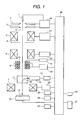
- FIG. 1 is a block diagram showing an embodiment of a scanning electron microscope in accordance with the present invention.
- a voltage is applied between a cathode 1 and a first anode 2 by a high voltage control power source 20 controlled by a computer 40 to extract a primary electron beam 4 with a preset emission current from the cathode 1.
- An acceleration voltage is applied between the cathode 1 and a second anode 3 by the high voltage control power source 20 controlled by the computer 40, and the primary electron beam 1 emitted from the cathode 1 is accelerated and travels to a lens system in the rear stage.
- the primary electron beam 4 is focused by a focusing lens 5 controlled by a lens control power source 21. Then, after unnecessary regions of the primary electron beam are removed by an aperture plate 8, the primary electron beam 4 is focused on a sample 10 as a very small spot by a focusing lens 6 controlled by a lens control power source 22 and an objective lens 7 controlled by an objective lens control power source 23.
- the objective lens 7 may be of various type such as an in-lens type, an out-lens type, a snorkel type (a semi-in-lens type) etc. Further, each of the lenses may be constructed of an electrostatic lens which is composed of a plurality of electrodes.
- the primary electron beam 4 is two-dimensionally (in X-Y directions) scanned on the sample 10 by a scanning coil 9. Current is supplied to the scanning coil 9 from a scanning coil control power source. Secondary signals 12 generated from the sample 10 by irradiation of the primary electron beam are travel to the upper portion of the objective lens 7, and then are separated from the primary electrons by a secondary signal separation orthogonally-crossing electro-magnetic field generator 11 to be detected by a secondary signal detector 13. The signals detected by the secondary signal detector 13 are amplified by a signal amplifier 14, and then transmitted to an image memory 25 and displayed on an image display unit 26 as a sample image.
- the secondary signal detector may be a detector for detecting secondary electrons or reflected electrons, or a detector for detecting light or X-rays.
- An address signal corresponding to a memory area of the image memory 25 is generated in a computer 40, and converted to an analogue signal, and than supplied to the scanning coil 9 though the scanning coil control power source 24.
- the address signal in X-direction is a digital signal repeating, for example, 0 to 512 in a case where the image memory 25 is 512 X 512 pixels
- the address signal in Y-direction is a digital signal repeating 0 to 512 which is added by 1 when the address signal in X-direction reaches 512 from 0.
- the signals are converted to the analogue signals.
- the address of the image memory 25 corresponds to the address of the reflection signal for scanning the primary electron beam
- a two-dimensional image of the deflection region of the primary electron beam by the scanning coil 9 is recorded in the image memory 25.
- the signals in the image memory 25 can be sequentially and successively read out using a read-out address generating circuit (not shown) synchronized by a read-out clock.
- the signal read-out corresponding to the address is converted to an analogue signal, and becomes a brightness modulated signal for the image display unit 26.
- the image memory 25 has a function for superposing (adding) the images (image data items) in order to improve the S/N ratio and then storing the composite image. For example, by superposing images obtained by 8 times of two-dimensional scanning and then storing the composite image, one frame of complete image is formed. That is, a final image is formed by adding images which are formed by once or more times of X-Y scanning. Number of images (number of adding frames) for forming one frame of the complete image may be arbitrarily set, and an appropriate number is set in taking into consideration conditions such as secondary electron generating efficiency and so on. Further, by superposing a plurality of frames each of which is formed by adding the plurality of images, a finally desired image may be formed. By executing blanking of the primary electron beam at the time when a desired number of image frames are stored or after the time, information input to the image memory may be interrupted.
- the number of adding frames is set to 8
- a two-stage deflecting coil 51 (an image shift deflector) is arranged at a position the same as that of the scanning coil 9, and thereby, the position of the primary electron beam 4 (the observed area) on the sample 10 can be two-dimensionally controlled.
- the deflecting coil 51 is controlled by a deflecting coil control power source 31.
- a stage 15 can move the sample 10 at least in 2 directions (X-direction and Y-direction) on a plane normal to the primary electron beam.
- an image acquiring condition (scanning speed, number of adding flames of image) and a method of correcting view area can be specified, and outputting and storing of the images can be also specified.
- the embodiment of the apparatus in accordance with the present invention comprises a function for forming a line profile based on detected secondary electrons or detected reflected electrons.
- the line profile is formed based on an amount of detected electrons when the primary electron beam is one-dimensionally or two-dimensionally scanned or based on brightness information of the sample image, and the obtained line profile is used for dimension measurement of a pattern formed, for example, on a semiconductor wafer.
- the embodiment of the apparatus in accordance with the present invention may further comprise an interface 41 for transmitting image data to an external unit or the like, and a recording unit 27 for storing image data to an appropriate memory medium.
- control unit is described as a unit integrated with the scanning electron microscope or the like, but it is, of course, not limited to such a unit.
- a control processor separately provided from the scanning electron microscope may be used to execute the processing as described below.
- a transmitting medium for transmitting signals from the control processor to the scanning electron microscope and input and output terminals for inputting and outputting the transmitted signals through the transmitting medium are necessary.
- a program for executing the processing to be described below is registered in a memory medium, and the program is executed by the control processor for supplying necessary signals to the scanning electron microscope having an image memory. That is, the embodiments of the present invention to be described below also hold as the invention of program which can be employed to a charged particle beam apparatus such as a scanning electron microscope having an image processor.
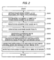
- FIG. 5 is a view schematically showing the processing of FIG. 2.
- Number N0 of adding frames for each acquired image and number N1 of acquired image sheets are specified. At that time, total number of adding frames of the final image is N0 X N1.
- the number N0 may be set to 1 frame.
- the number N0 can be set to 2.
- the condition setting it is preferable that the plurality of sample images are formed by fixing the optical conditions (a focusing condition of the electron beam and a scanning condition) in order to make detection of positional displacement easy.
- N1 sheets of images of frame adding number N0 F1, F2, ..., FN1 in the same view area are successively acquired.
- F1 is set to a memory area of the objective image F0.
- a sharpened image F0a is produced from the objective image F0.
- a technique using an image filter for emphasizing edges in the image may be used.
- a sharpened image F2a is produced from the image F2.
- a positional displacement between the sharpened image F2a of F2 and the sharpened image F0a is detected.
- Calculation processing such as image correlation may be applied to the detection of the positional displacement.
- the present invention is not limited to the above, and all the image processing methods capable of detecting the positional displacement are applicable.
- Pixels of the original image F2 is shifted by the amount of the displacement of view area detected in the Sixth Step and added to the image of F0, and then the formed image is returned as the objective image F0 again.
- the finally obtained image is an image formed by adding N0 X N1 frames, but the image is blurred by the drift only when N0 frames are added. Therefore, the blur of the image by the drift is reduced to 1/N1 compared with the case of directly adding N0 X N1 frames.
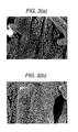
- FIG. 3 shows an example of a result obtained by this embodiment.
- FIG. 3 (a) is an image obtained through commonly adding the frames (1280 X 960 pixels, 200 thousands times of magnification), and drifts are accumulated during adding the images to form conspicuous "blur" in the final image.
- FIG. 3 (b) is an image obtained by acquiring 10 sheets of images having frame adding number 1/10 times as small as the frame adding number of FIG. 3 (a), and adding these 10 sheets of the images while the positional displacements are being corrected.
- the "blur" in the final image caused by the drift is also reduced to 1/10 times as small as that in FIG. 3 (a) because only the drift accumulated each of the added image becomes “blur” in the final image and the acquiring time for each image is 1/10 times as short as that in FIG. 3 (a).
- N0 and N1 are set corresponding to the S/N ratio. Since number of scanning times (number of images) required for securing a required S/N ratio is determined based on the quality of obtained image and the efficiency of generating secondary electrons, N0 and N1 may be determined in taking the degree of drift into consideration. Further, it is also possible to construct the sequence that by inputting a parameter expressing conditions of the sample (easiness of charge-up etc) and at least one of total adding number, number of adding frames (N0) and number of acquired images (N1), the other two parameters are determined. According to such a construction, the apparatus condition can be easily set only by inputting specification necessary for observation.
- correction of the positional displacement may be executed by the unit of an arbitrary number of frames or by the unit of arbitrary number of acquired sheets.
- N0 the frame adding number
- N1 number of acquired image sheets
- the image may be stored in the image memory 25 after correcting the positional displacement. Otherwise, by preparing a frame memory corresponding to (frame adding number) X (acquired images), the positional displacement among sample images may be corrected when the sample image is displayed, or when the sample image is transferred to an external image memory element, or before the sample image is transferred to the external image memory element. Otherwise, the positional displacement among sample images may be corrected in the external image memory element.
- an image memory for storing images before executing superposing processing and an image memory for storing an image to be acquired images acquired one after another by the electron beam scanning can be successively superposed.
- the system in order to make the setting of N0 and N1 for specified samples easier, the system may be constructed in such that a reference image for each combination of N0 and N1 is stored, and the reference image can be read out at setting N0 and N1. By doing so, an operator can set appropriate N0 and N1 by referring to the reference image.
- N0 when drift is fast, number of displacement corrections is increased by decreasing number of frames N0, and that when drift is nor so fast, number of frames N0 is increased in order to improve the quality of the image to be compared with.
- a means for adjusting N0 and N1 stepwise is provided as a means for appropriately setting numbers of N0 and N1.
- the combinations of N0 and N1 are 1 X 50, 2 X 25, 5 X 10, 10 X 5, 25 X 2 and 50 X 1.
- the operator can set appropriate N0 and N1 from the superposed image without detailed knowledge on the technology in regard to the present invention.
- the same effect can be attained by providing a means for adjusting the degree of displacement correction which sets N1 to a larger value when "the degree of displacement correction is large” is selected, and sets N0 to a smaller value when "the degree of displacement correction is small” is selected.
- FIG. 4 A processing flow of FIG. 4 will be described below in detail.
- Number N0 of adding frames for each acquired image and number N1 of acquired image sheets are set.
- Sharpened images are generated from the acquired two sheets of images, and a positional displacement between the sharpened images is calculated.
- each of the images before correcting the position and being added conspicuously includes "blurs" due to drift. Therefore, the processing is stopped, and a display function may notify the operator that the drift is too large.
- the two sheet of images after correcting the positional displacement are added to each other, and the added image is registered as F0.
- each of a method of using an electric view-area shifting means (an image shift deflector) and a method of using a stage is available depending on the amount of shifting.
- an image shift deflector an image shift deflector
- a method of using a stage is available depending on the amount of shifting.
- the amount of shifting is small, both of the image shift deflector and the stage are used.
- the stage is used or the image shift deflector is used if necessary.
- the next image is acquired.
- the image F0 and the image acquired in S4006 are added by correcting the positional displacement between the images, and the added image is newly set as F0.
- the view area is moved in a direction canceling the positional displacement obtained in the process of S4008.
- a large drift component can be corrected by the stage and the beam deflection, and very small drift of pixel level can be corrected at adding the images. Therefore, a high resolution image can be obtained by effectively correcting even a comparatively large drift.
- the limit is determined by the S/N ratio of the images necessary for deteuting the positional displacement. Therefore, if the amount of the drift exceeds a certain value, each of the images itself for detecting the positional displacement becomes blurred due to drift. When an amount of drift causing such a result is detected, a means for displaying that a high resolution image is difficult to be acquired or for stopping the measurement may be provided. By doing so, it is possible to solve a problem of uselessly operating the apparatus under a state that acquiring of the sample images is clearly difficult.
- FIG. 6 A processing flow of FIG. 6 will be described below in detail.
- a first image F1 for detecting drift is acquired.
- An objective image F0 is acquired under an appropriate slow scanning condition.
- a high contrast image can be obtained because secondary electrons can be generated more compared to the case of fast scanning.
- a second image F2 for detecting drift is acquired.
- a displacement ⁇ F ( ⁇ Fx, ⁇ Fy) between the images F1 and F2 is detected.
- Amounts of deformations in the horizontal direction and the vertical direction of the objective image are calculated from the amount of image displacement ⁇ F.
- a new image F0' is formed by deforming the objective image F0.
- drift speeds (Vx, Vy) in X-direction and Y-direction can be calculated by the following equations.
- Vx ⁇ Fx / ⁇ T
- Vy ⁇ Fy / ⁇ T
- X-direction ⁇ F0x Vx X T0
- Y-direction ⁇ F0y Vy X T0
- the images F1 and F2 for detecting drift are acquired before and after acquiring the objective image F0, respectively, but, of course, the present invention is not limited to the above.
- the images F1 and F2 may be successively acquired before acquiring the image F0 or after acquiring the image F0. In that case, the deformation is estimated from the displacement between the images F1 and F2 at the time when the image F0 is acquired, and then the estimated image F0' can be reproduced.
- Each of the images F1, F2 and F0 is stored in the image memory, and the images F1 and F2 are read out based on judgment on necessity of image reproduction, and then the reproduction processing is performed.
- the shape of an observed object deformed by drift can be accurately known.
- the present embodiment has been described on the case of two images for correcting drift and one image to be corrected, the present invention is not limited to the above and arbitrary number of images may be used.
- GUI graphical user interface
- FIG. 16 shows the example of performing selection using a pointing device or the like on the image display unit, the present invention is not limited to this method. Setting may be performed using another well-known input setting means.
- the sample image is highly accurately formed.
- damage of the sample is reduced by suppressing irradiation of the electron beam as low as possible.
- the sample image can be firmed with high accuracy if the deformation of the sample due to drift can be suppressed, but the electron beam scanning for acquiring at least the images F1 and F2 is further required, which is different from the case of simply forming the image F0. That is, since the scanning time of the electron beam is increased, possibility of the sample damage caused by7 the electron beam irradiation is increased,
- the operator can select necessity of the reproduction taking a status of the observed object or the condition for forming an appropriate sample image into consideration, and can form the sample image which the operator desires.
- the information can be used for setting the scanning speed and for judgment of necessity of drift correction. Further, by storing and displaying number of scanning times of the electron beam and amount of correction and the amount of deformation versus the irradiation time, it is possible to know the sample image is deformed by how long the electron beam is scanned.
- measurement of dimension of a pattern on a wafer uses a signal distribution (a line profile) which is obtained when an electron beam is line-scanned on a pattern of a measured object.
- a signal distribution a line profile
- the sample is an insulator
- high speed scanning is performed in order to prevent disturbance caused by charging. Therefore, since a signal obtained by once of line scanning is bad in the S/N ratio, it is difficult to perform highly reproducible measurement.
- signal distributions obtained from several times of scanning are added to form a profile of the measured object. At that time, if drift occurs in the direction of line scanning, the added line profile becomes dull, and accordingly the accuracy of measurement is decreased.
- each of the profiles obtained by plural times of line scanning is stored, and positional correction of the profiles is performed so that the correlation among the profiles becomes highest, and then the profiles are added.
- a signal acquired by once of scanning may be used as each of the profiles before addition.
- the scanning speed is high, the signal acquired by once of scanning is too bad in the S/N ratio. Therefore, signals obtained by minimum number of scanning times within a range capable of correlating among the profiles are simply added, and the added signal may be used as each of the profiles before addition.
- the problem of dullness of the profile is improved even if there is drift, and a profile having a high S/N ratio can be produced. Therefore, it is possible to perform highly reproducible measurement.
- the apparatus may be constructed in such that the setting page described in FIG. 16 is also used for selecting the necessity of positional correction.
- a semiconductor inspection apparatus or the like may be constructed in such that reliability of the measurement can be checked later by sounding an alarm or setting a flag to the measurement when an amount of positional correction exceeds a threshold and clearly increases.
- the apparatus may be constructed in such that the added image or the images before adding are stored and displayed on an image display unit later.
- the measurement can be rapidly performed compared to the case of two-dimensional scanning.
- the line profile can be formed with high accuracy even in the case of one-dimensional scanning by which the measurement can be rapidly performed.
- the length can be measured with high accuracy based on the line profile formed with high accuracy.
- the measuring length range is expanded toward directions perpendicular to the direction of measuring length, and measurement of length based in the line profile is performed using a plurality of different positions within the measuring length range. Then, the plurality of obtained measured length values are averaged, or the dispersion values of roughness are measured based on the plurality of measured length values obtained within the expanded measuring length range.
- the present embodiment is also applicable to this case.
- the added line profile can be appropriately formed and the length can be accurately measured by performing positional correction, using one reference line profile, to the line profiles in the other positions, not by performing positional correction for each of the plurality of the length measuring positions. According to the construction described above, reliability evaluation of electric property of a semiconductor element pattern can be easily realized regardless of existence of roughness.
- the apparatus may be constructed in such that an error message is output or that the measured results such as the sample image and the line profile are registered together with the measuring conditions so as to check the results later by read out the data.
- FIG. 9 is a graph for explaining an example of estimating an accurate dimension from time-varying pattern dimensions by repeating measurement of the same pattern plural times.
- the object to be measured using an electron beam is damaged to be shrunk or evaporated depending on the material by irradiation of the electron beam.
- the pattern dimension is decreased as the amount of beam irradiation increases, the measurement itself is an error cause.
- the same pattern is measured plural times. Since the amount of beam irradiation is increased in proportion to number of measuring times, deformation of the pattern is also increased as the number of measuring times is increased. Therefore, the pattern dimension before irradiating the beam or before shrinking at starting the beam irradiation can be estimated by obtaining the relationship between the number of measuring times (in proportion to the amount of beam irradiation) and the dimension measured value.
- a sequence for automatically executing the above-described dimension estimation is installed.
- the apparatus may be constructed in such that in order to judge later whether or not the dimension estimation is correctly performed, a table graphing number of measuring times versus measured value is stored, and then output to the display unit or an external output unit. For example, in a case where an observed object is shrunk and at the same time drift also occurs, the dimension estimation may be not appropriately performed by influence of the drift, the operator can check by referring to the above-described graph whether or not the dimension estimation is correct. By storing a sample image obtained at that time corresponding to the stored graph, the correctness of the dimension estimation can be checked referring to the sample image.
- the apparatus may be constructed in such that when the above-described graph records an abnormal trend, the graph is selectively stored or a preset flag is set. For example, when an abnormal change is observed in a graph expressing the trend of dimension change, something may occur in the electron beam apparatus at that time, and accordingly the dimension measurement may be not correctly performed. If the apparatus is constructed so that the graph or the sample image can be selectively checked at that time, the operator can efficiently check the correctness of the dimension estimation without performing useless check.
- the abscissa of the graph expresses "number of measuring times” in the present embodiment, the abscissa may express another parameter such as “number of scanning times” or "time”.
- the ordinate is not limited to express "measured value” either, and the ordinate may express a ratio of a measured value to a normal value (a design value).
- FIG. 10 is a view showing an example in which images, each of which has number of pixels larger than number of pixels of an objective image, are acquired, and displacements among the acquired images are corrected.
- the number of pixels of the objective image is, for example, 512 X 512 pixels.
- the number of pixels of the acquired image is 1024 X 1024 pixels.
- FIG. 11 shows an embodiment in which images are added by removing an abnormal images.
- an abnormally displaced image or an abnormally blurred image is formed by a sporadic disturbance during acquiring a plurality of images, or in a case where images acquired after acquiring a specific image show abnormal contrast due to charge during irradiating the beam
- the abnormal image can be removed from the original images to be added by detecting the abnormality through image processing of these images.
- displacement the abnormality can be detected by presetting an amount of displacement of view area to be judged as abnormal.
- the abnormal image can be removed by executing image differential processing or the like, and setting a threshold to be judged as abnormal.
- the abnormal image can be removed by judging on a histogram or by judging on abnormal decrease in the value of correlation with another image after correcting view area.
- the image judged to be abnormal can be removed, in order to search the cause of abnormality later, the image judged to be abnormal is stored in the image memory together with the optical conditions (acceleration voltage of the electron source, emission current and so on) at the time when the abnormality is recognized, or before and after the time when the image is judged to be abnormal.
- the optical conditions acceleration voltage of the electron source, emission current and so on
- Changes of current and voltage applied to the optical element such as the extracting electrode, the acceleration electrode or the scanning coil of the electron microscope are displayed by a time chart, and the timing that the abnormality occurs is superposed on the time chart. By doing so, the operator can visually specify the cause.
- the abnormal frame removing technology explained by the present embodiment can be applied to the line profile addition explained in Embodiment 4.
- the present invention is not limited to the above.
- the apparatus is constructed in such that some of images can be selected using a pointing device or the like from the plurality of images before adding arranged and displayed on the image display unit, the operator can be visually select images to be removed from the plurality of images before adding.
- the apparatus may be constructed in such that not only the images before adding are displayed, but also the plurality of added images are displayed in order to ascertain abnormal images using the images having a some degree of S/N ratio.
- FIG. 12 shows an embodiment in which view area displacements among a plurality of images acquired by a plurality of image signals are corrected, and then the images are added. For example, when an added image using reflected electron signal is tried to be acquired, a lot of frames must be acquired for each of the original images because the amount of the reflected electron signal is generally little. The reason is that if an original image is formed by acquiring a small number of image frames acquired by the small signal amount, the view area displacement among the images can not detected because the S/N ratio of the original image is extremely decreased. On the other hand, if number of the original image frames is increased, the original image itself is blurred due to drift because the time acquiring the original images becomes long.
- the original images are acquired by the reflected electron signal, and at the same time original images having a good S/N ratio are acquired using secondary electron signal, and view area displacement among the original images acquired by the secondary electron signal is detected, and then the amount of the detected view area displacement is applied to the view area displacement among the plurality of images obtained by the reflected electron signal.
- the view area displacement of the original reflected electron images having a bad S/N ratio can be accurately corrected through the method of the present embodiment. Since the secondary electron signal image having a high S/N ratio is used as the image for detecting the view area displacement, number of frames composing the original image can be minimized. Therefore, the original image itself is not blurred by drift.
- signal having a bad S/N ratio there are, for example, X-ray signal and sample absorption current.
- the embodiment of the present invention can be applied to various kinds of signals.
- the secondary electron signal in the present embodiment may be replaced by transmission electron signal.
- occurrence of X-rays scattering inside a sample can be prevented by making the sample into a foil having a thickness of several tens nm, and accordingly a high resolution element distribution image can be obtained.
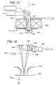
- FIG. 17 As the detection system for detecting secondary electrons and reflected electron at the same time, a construction shown in FIG. 17 is considered. According to this construction, two kinds of electrons (reflected electrons 1706, secondary electrons 1707) emitted from a sample 1705 can be detected at the same time using a reflected electron detector 1703 and a secondary electron detector 1704 arranged at an upper position and at a lower position of an objective lens 1702 for focusing a primary electron beam 1701, respectively.
- a reflected electron detector 1703 and a secondary electron detector 1704 arranged at an upper position and at a lower position of an objective lens 1702 for focusing a primary electron beam 1701, respectively.
- secondary electrons and reflected electrons can be detected together using a detection system shown in FIG. 18.
- secondary electrons and reflected electrons 1803 are accelerated by a retarding voltage 1802 applied to a sample 1801, and collide against a secondary electron converting electrode 1805 arranged above an objective lens 1804.
- the accelerated secondary electrons and the accelerated reflected electrons 1803 produce secondary electrons 1806, and the secondary electrons 1806 are attracted to a secondary electron detector 1807 to be detected.
- An energy filter 1808 is applied with an energy filter voltage 1809 which is equal to or slightly higher than the retarding voltage 1802 applied to the sample. By applying such a voltage, only the reflected electrons are selectively pass through the energy filter 1808.
- the secondary electrons and the reflected electrons are alternatively acquired by switching the voltage of the energy filter 1809 on-off or strong-weak every acquiring of predetermined number of two-dimensional image frames. Then, the positional displacement is detected using the secondary electron images, and the positional displacement of the reflected electron image is corrected using the detected positional displacement information, and then the reflected electron image is stored in the image memory. By doing so, in the scanning electron microscope employing the retarding technology, the reflected electron image without blur can be obtained. Although the reflected electrons and the reflected electrons are clearly separated in the present embodiment, the present invention is not limited to the above.
- the amount of electrons detected by the secondary electron detector 1809 may be increased by applying an energy filter voltage 1809 lower than the retarding voltage 1802 to the energy filter 1808. Since most of the electrons emitted from the sample have energy smaller than 50 eV, number of frames composing the original image can be minimized by using electrons having energy smaller than 50 eV for the images for detecting the view area displacement.
- the applied voltage to the energy filter 1808 may be changed depending on the purpose of analysis.
- the reflected electron detector and the secondary electron detector are not limited to those described in the present embodiment, but various types of detectors may be employed. Although the X-ray detector has not been illustrated, all of the existing X-ray detectors are applicable.
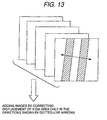
- FIG. 13 shows an embodiment in which positional displacements of a plurality of acquired images are corrected only in a specified direction on a sample surface, and then the images are added.
- positional displacement in a direction perpendicular to the pattern can be detected with high accuracy, but accuracy of detecting positional displacement in a direction parallel to the pattern is extremely low.
- the error in the view area adjusting can be reduced.
- the direction of the pattern can be specified by analysis of frequency components of the image or line profiling of the image by binarization.
- FIG. 14 shows a method of detecting the amount of positional displacement and adding the corrected images.
- a region 1403 having an adequate size is put, for example, in the central portion of the input image 1401, and template matching is performed to the input image 1402 using the area 1403 as a template.
- a region 1404 matches with the region 1403 as the result, the region 1403 and the region 1404 are overlapped on each other, and a rectangular region (an AND region) 1405 of overlapping the input image 1401 and the input image 1402 on each other is set, and a portion not overlapping with the AND region in each of the input image 1401 and the input image 1402 is cut off to form a post-position-adjusting input image 1406 or 1407, respectively.
- Adding processing is performed by inputting the post-position-adjusting input images 1406 and 1407.
- This example shows the case of two input images, but it is easy to extend to a case of three or more input images.
- the template matching there is a method of executing normalized correlation processing between two images based on the following equation, where the size of the input image is assumed to be 512 X 512 pixels and the size of the template in the center is assumed to be 256 X 256 pixels. Therein, a position where the calculated correlation value becomes the maximum is defined as a matching position.
- r(x, y) is a correlation value at (x, y)
- M ij is a density value at a point (i, j) inside the template
- P ij is a density value at a corresponding point (x+1, y+1) of the input image
- N is number of pixels of the template.
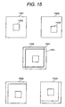
- FIG. 15 shows another embodiment of a method of adding corrected images.
- a region 1403 having an adequate size is put, for example, in the central portion of the input image 1401, and template matching is performed to the input image 1402 using the area 1403 as a template.
- a region 1404 matches with the region 1403 as the result, the region 1403 and the region 1404 are overlapped on each other, and a rectangular region (an OR region) 1501 including both of the input image 1401 and the input image 1402 is set, and a portion not overlapping with the OR region in each of the input image 1401 and the input image 1402 is added, and each of the added portions is filled with number of pixels of 0 or an average value of each of the input images to form a post-position-adjusting input image 1502 or 1503, respectively.
- Adding processing is performed by inputting the post-position-adjusting input images 1502 and 1503. This example shows the case of two input images, but it is easy to extend to a case of three or more input images.
- drift correction technology in accordance with the present invention is applied to automatic operation of a semiconductor inspection scanning electron microscope.
- a recipe file to which information such as measuring positions and observing conditions is registered is formed in advance, and then measurement positioning, observation and measurement are performed according to the file.
- an environment set before executing the recipe file is registered.
- FIG. 19 shows a recipe execution environment page.
- Main sequence of executing the recipe is as follows. That is, initially, alignment for detecting a position of a wafer on a stage is executed. At that time, image recognition is performed according to an image registered at forming the recipe. Next, the wafer is moved to the measuring position using the stage, and an image is acquired with a comparatively low magnification. Positioning of the measured pattern (called as addressing) is performed with high accuracy by image recognition, and pattern dimension measurement is performed by electrically deflecting the electron beam and zooming up to the measuring magnification. Automatic focus adjustment is performed before the positioning of the pattern or before the measurement.
- an amount of drift during the time period from acquiring of an image for positioning the pattern to acquiring an image for measurement is measured for each of the measured points using the first wafer.
- an amount of drift at several minutes after the alignment is measured and stored.
- an amount of drift at each of the measured points or the alignment point is added to the image as an offset after positioning.
- the electron beam is deflected to a position added with the offset and the magnification is zoomed up to the measuring magnification.
- the drift after positioning can be reduced, and the plurality of samples can be measured with high throughput because it is unnecessary to detect the amount of drift at the actual measurement using the recipe or at measuring the second wafers and wafers after the second.
- the drift correction is executed at alignment, at addressing or at measurement is judged by ON or OFF of a drift correction switch 1901 for alignment, a drift correction switch 1902 for addressing or a drift correction switch 1903 for measurement, respectively.
- a plurality of semiconductor wafers are usually dealt by the cassette unit by containing the semiconductor wafers in a cassette.
- An apparatus for continuously measuring such a plurality of measured objects is provided with a means for selecting whether or not drift correction is performed based on an amount of correction registered at forming the recipe and a means for selecting whether or not drift correction is performed based on an amount of drift actually measured each wafer.
- a means for selecting whether or not offset correction is performed based on a value registered at forming the recipe and a means for selecting whether or not offset correction is performed using a value used for detecting the amount of drift in the first wafer in the cassette and registered are provided.
- the present invention is not limited to the above.
- the present invention is not limited to the scanning electron microscope.
- the present invention can be applied to a charged particle beam apparatus of another type in which a sample image is displaced due to some drift producing cause.
Landscapes
- Chemical & Material Sciences (AREA)
- Analytical Chemistry (AREA)
- Life Sciences & Earth Sciences (AREA)
- Computer Vision & Pattern Recognition (AREA)
- Physics & Mathematics (AREA)
- Health & Medical Sciences (AREA)
- Engineering & Computer Science (AREA)
- Biochemistry (AREA)
- General Health & Medical Sciences (AREA)
- General Physics & Mathematics (AREA)
- Immunology (AREA)
- Pathology (AREA)
- Length-Measuring Devices Using Wave Or Particle Radiation (AREA)
- Testing Or Measuring Of Semiconductors Or The Like (AREA)
Abstract
Description

Claims (21)
- A method of forming a sample image by scanning a charged particle beam on a sample and forming an image based on secondary signals emitted from said sample, the method comprising the steps of:forming a plurality of composite images by superposing a plurality of images obtained by a plurality of scanning times; andforming a further composite image by correcting positional displacements among said plurality of composite images and superposing said plurality of composite images.
- A method of forming a sample image by scanning a charged particle beam on a sample and forming an image based on secondary signals emitted from said sample, the method comprising the steps of:two-dimensionally scanning said charged particle beam on said sample;detecting secondary signals emitted from a scanned region;forming image data based on said detected secondary signals;forming a plurality of composite image data items formed by superposing said plurality of image data items;detecting positional displacements in said two-dimensional directions among said plurality of formed composite image data items; andforming an image by correcting said detected positional displacements.
- A charged particle beam apparatus comprising a charged particle source; a deflector for scanning a charged particle beam emitted from said charged particle source; and a detector for detecting secondary signals emitted from a scanned region of said charged particle beam, a sample image being formed based on said secondary signals detected by said detector, which further comprises:a control unit which forms a plurality of image data items based on said detected secondary signals, and forms a plurality of composite image data items by superposing said plurality of image data items, and corrects displacements among said plurality of composite image data items, and then superposes said plurality of composite image data items.
- A charged particle beam apparatus according to claim 3, wherein said plurality of composite image data items are formed by the unit of two-dimensional scanning performed by said deflector.
- A charged particle beam apparatus according to claim 3, wherein said plurality of composite image data items are acquired in different timing from one another.
- A charged particle beam apparatus according to claim 3, which further comprises
an image shift deflector for shifting a scanning region of said charged particle beam; and
a sample stage for shifting said sample, wherein
said control unit detects directions of displacements among said images, and operates said image shift deflector and/or said sample stage so that said scanning regions may be positioned toward directions canceling said displacements. - A charged particle beam apparatus according to claim 6, wherein
said control unit shifts said scanning region using said sample stage and/or said image shift deflector when an amount of said displacement is larger than a preset value, and shifts said scanning region using said image shift deflector when an amount of said displacement is smaller than the preset value. - A charged particle beam apparatus according to claim 3, which further comprises an image sharpening means for sharpening said image to be superposed, and a displacement between said image data items is detected based on image data sharpened by said image sharpening means.
- A charged particle beam apparatus according to claim 3, wherein number of pixels of said composite image data formed by superposing said plurality of image data items is larger than number of pixels of the image data before being superposed.
- A method of forming a sample image by scanning a charged particle beam on a sample and forming an image based on secondary signals emitted from said sample, the method comprising the steps of:two-dimensionally scanning said charged particle beam on said sample;detecting secondary signals emitted from a scanned region;forming at least three images based on said detected secondary signals;by using at least two of said three images, detecting deformation or positional displacement in the other one of said three images; andcorrecting deformations or displacements of said image based on said detected deformation.
- A charged particle beam apparatus comprising a charged particle source; a deflector for scanning a charged particle beam emitted from said charged particle source; and a detector for detecting secondary signals emitted from a scanned region of said charged particle beam, a sample image being formed based on said secondary signals detected by said detector, which further comprises:a control unit for two-dimensionally scanning said charged particle beam on said sample; detecting secondary signals emitted from a scanned region; forming at least three images based on said detected secondary signals; by using at least two of said three images, detecting deformation or positional displacement of the other one sheet; and correcting deformations or displacements of said image based on said detected deformation.
- A method of measuring a dimension of sample by scanning a charged particle beam on a sample, and forming a line profile based on secondary signals emitted from said sample, and measuring a dimension of a measured object on said sample from said line profile, the method comprising the steps of:scanning said charged particle beam on said sample;detecting secondary signals emitted from a scanned positions;forming a plurality of line profiles based on said detected secondary signals;detecting positional displacements among said plurality of line profiles;superposing said plurality of line profile by correcting said displacements, andmeasuring a dimension of said measured object based on said composite line profile.
- A charged particle beam apparatus comprising a charged particle source; a deflector for scanning a charged particle beam emitted from said charged particle source; and a detector for detecting secondary signals emitted from a scanned region of said charged particle beam, a line profile being formed based on said secondary signals detected by said detector, a dimension of a measured object being measured based on said line profile, which further comprises:a control unit for scanning said charged particle beam on said sample; detecting secondary signals emitted from a scanned positions; forming a plurality of line profiles based on said detected secondary signals; detecting positional displacements among said plurality of line profiles; superposing said plurality of line profile by correcting said displacements, and measuring a dimension of said measured object based on said composite line profile.
- A method of measuring a dimension of sample by irradiating a charged particle beam on a sample, and measuring a dimension of a measured object formed on said sample based on secondary signals emitted from said sample, the method comprising the steps of:measuring decreasing change of a dimension of said measured object which decreases as said sample is being irradiated with said charged particle beam; andcalculating a dimension of said measured object before or at starting irradiating said charged particle beam from said decreasing change.
- An electron beam apparatus comprising a charged particle source; a deflector for scanning a charged particle beam emitted from said charged particle source; and a detector for detecting secondary electrons emitted from a scanned region of said electron beam, which further comprises:a reflected electron detector for detecting reflected electrons emitted from said sample and/or an X-ray detector for detecting X-rays emitted from said sample; andan image display unit for display a sample image based on reflected electrons detected by said reflected electron detector or X-rays detected by said X-ray detector, whereina shifting amount of a secondary electron image detected by said secondary electron detector is detected, and a position of a reflected electron image or an X-ray image displayed on said image display unit is corrected based on said shifting amount of the secondary electron image.
- A method of forming a sample image by scanning a charged particle beam on a sample and forming an image based on charged particles emitted from said sample, the method comprising the steps of:scanning said charged particle beam on said sample plural times;obtaining a plurality of images based on detection of secondary signals emitted from said sample based on said plural times of scanning;removing images having abnormality from said plurality of images; andsuperposing said plurality of images excluding said images having abnormality to form a composite image.
- A charged particle beam apparatus comprising a charged particle source; a deflector for scanning a charged particle beam emitted from said charged particle source; and a detector for detecting secondary signals emitted from a scanned region of said charged particle beam, a sample image being formed based on said secondary signals detected by said detector, which further comprises:a control unit which forms a plurality of image data items based on said detected secondary signals, and removing image data items having abnormality from said plurality of image data items, andsuperposing said plurality of images excluding said image data items having abnormality.
- A method of forming a sample image by scanning a charged particle beam on a sample and forming an image based on charged particles emitted from said sample, the method comprising the steps of:selectively correcting displacements in a specific direction among a plurality of images obtained by plural times of scanning; andsuperposing said plurality of corrected images to form a composite image.
- A method of forming a sample image according to claim 18, wherein
said specific direction is a direction intersecting at right angle with a longitudinal direction of a line pattern formed on said sample. - A charged particle beam apparatus comprising a charged particle source; a deflector for scanning a charged particle beam emitted from said charged particle source on a sample; a detector for detecting secondary signals emitted from a scanned region of said charged particle beam, an image memory for storing a sample image formed based on charged particles detected by said detector, wherein
said image memory is constructed so as to add a plurality of sample images and then to store said added sample image, and comprises means for correcting displacements of said sample images to be added and performing said addition; and means for setting a condition of said addition. - A charged particle beam apparatus comprising a charged particle source; a deflector for scanning a charged particle beam emitted from said charged particle source; and a detector for detecting secondary signals emitted from a scanned region of said charged particle beam, a sample image being formed based on said secondary signals detected by said detector, which further comprises:means for forming N0 frames of image data items based on said detected secondary signals, and for forming N1 frames of composite image data items by superposing said N0 frames of image data items; andsetting means for setting said N0 and said N1.
Applications Claiming Priority (1)
| Application Number | Priority Date | Filing Date | Title |
|---|---|---|---|
| PCT/JP2001/010168 WO2003044821A1 (en) | 2001-11-21 | 2001-11-21 | Sample imaging method and charged particle beam system |
Publications (3)
| Publication Number | Publication Date |
|---|---|
| EP1455378A1 true EP1455378A1 (en) | 2004-09-08 |
| EP1455378A4 EP1455378A4 (en) | 2011-01-26 |
| EP1455378B1 EP1455378B1 (en) | 2013-08-14 |
Family
ID=32800783
Family Applications (1)
| Application Number | Title | Priority Date | Filing Date |
|---|---|---|---|
| EP01274171.6A Expired - Lifetime EP1455378B1 (en) | 2001-11-21 | 2001-11-21 | Sample imaging method and charged particle beam system |
Country Status (3)
| Country | Link |
|---|---|
| US (2) | US7034296B2 (en) |
| EP (1) | EP1455378B1 (en) |
| JP (1) | JP4065847B2 (en) |
Cited By (2)
| Publication number | Priority date | Publication date | Assignee | Title |
|---|---|---|---|---|
| EP2530699A4 (en) * | 2010-01-25 | 2014-06-04 | Hitachi High Tech Corp | Charged particle beam microscope and method of measurement employing same |
| CN107533017A (en) * | 2015-03-23 | 2018-01-02 | 泰科英赛科技有限公司 | The mthods, systems and devices related to distortion correction in imaging device |
Families Citing this family (34)
| Publication number | Priority date | Publication date | Assignee | Title |
|---|---|---|---|---|
| JP4069545B2 (en) * | 1999-05-19 | 2008-04-02 | 株式会社日立製作所 | Electron microscope method, electron microscope array biological sample inspection method and biological inspection apparatus using the same |
| US7361894B2 (en) * | 2002-10-22 | 2008-04-22 | Hitachi High-Technologies Corporation | Method of forming a sample image and charged particle beam apparatus |
| WO2003044821A1 (en) * | 2001-11-21 | 2003-05-30 | Hitachi High-Technologies Corporation | Sample imaging method and charged particle beam system |
| US7034296B2 (en) * | 2001-11-21 | 2006-04-25 | Hitachi High-Technologies Corporation | Method of forming a sample image and charged particle beam apparatus |
| DE10234404B4 (en) * | 2002-07-29 | 2021-10-14 | Leica Microsystems Cms Gmbh | Method, arrangement and software for monitoring and controlling a microscope |
| JP2004251829A (en) * | 2003-02-21 | 2004-09-09 | Hitachi High-Technologies Corp | Scanning electron microscope with length measuring function and length measuring method using the same |
| JP4383950B2 (en) * | 2004-04-23 | 2009-12-16 | 株式会社日立ハイテクノロジーズ | Charged particle beam adjustment method and charged particle beam apparatus |
| US7365310B2 (en) * | 2005-06-27 | 2008-04-29 | Agilent Technologies, Inc. | Increased depth of field for high resolution imaging for a matrix-based ion source |
| JP2007115587A (en) * | 2005-10-21 | 2007-05-10 | Sii Nanotechnology Inc | Charged particle beam processing method and charged particle beam apparatus |
| US7732765B2 (en) * | 2006-11-17 | 2010-06-08 | Hitachi High-Technologies Corporation | Scanning electron microscope |
| JP5638396B2 (en) * | 2008-01-22 | 2014-12-10 | アプライド マテリアルズ イスラエル リミテッド | System and method for material analysis of fine elements |
| JP2010017376A (en) * | 2008-07-11 | 2010-01-28 | Fujifilm Corp | Radiographic imaging apparatus |
| JP5286004B2 (en) * | 2008-09-12 | 2013-09-11 | 株式会社日立ハイテクノロジーズ | Substrate inspection apparatus and substrate inspection method |
| JP5080657B2 (en) | 2008-12-15 | 2012-11-21 | 株式会社日立ハイテクノロジーズ | Scanning electron microscope |
| JP5198654B2 (en) * | 2009-04-03 | 2013-05-15 | 株式会社日立ハイテクノロジーズ | Composite image creation method and apparatus |
| US9123502B2 (en) | 2009-05-20 | 2015-09-01 | Carl Zeiss Microscopy, Llc | Scan method |
| JP5668056B2 (en) * | 2009-05-20 | 2015-02-12 | カール ツァイス マイクロスコーピー エルエルシー | Scanning method |
| WO2011007492A1 (en) * | 2009-07-16 | 2011-01-20 | 株式会社日立ハイテクノロジーズ | Charged particle beam microscope and measuring method using same |
| JP5455694B2 (en) | 2010-02-09 | 2014-03-26 | 株式会社日立ハイテクノロジーズ | Charged particle beam equipment |
| JP5542478B2 (en) * | 2010-03-02 | 2014-07-09 | 株式会社日立ハイテクノロジーズ | Charged particle beam microscope |
| US8841612B2 (en) * | 2010-09-25 | 2014-09-23 | Hitachi High-Technologies Corporation | Charged particle beam microscope |
| JP5948074B2 (en) | 2012-02-13 | 2016-07-06 | 株式会社日立ハイテクノロジーズ | Image forming apparatus and dimension measuring apparatus |
| EP2660845A1 (en) * | 2012-05-02 | 2013-11-06 | FEI Company | Charged-particle microscopy with image stitching |
| JP5998004B2 (en) * | 2012-10-16 | 2016-09-28 | 株式会社日立ハイテクノロジーズ | Charged particle beam equipment |
| JP5758025B1 (en) * | 2014-04-30 | 2015-08-05 | 株式会社Pfu | Image reading device |
| CA3054601C (en) * | 2017-03-13 | 2023-02-28 | Zoetis Services Llc | A lateral flow test system |
| DE102017212214A1 (en) | 2017-07-17 | 2019-01-17 | Carl Zeiss Microscopy Gmbh | A method of recording an image using a particle microscope and particle microscope |
| DE102018124401A1 (en) | 2018-10-02 | 2020-04-02 | Carl Zeiss Smt Gmbh | Method for taking an image with a particle microscope |
| JP7162734B2 (en) | 2019-04-18 | 2022-10-28 | 株式会社日立ハイテク | Charged particle beam device |
| US11113827B2 (en) * | 2019-09-23 | 2021-09-07 | Kla Corporation | Pattern-to-design alignment for one-dimensional unique structures |
| CN115917438A (en) * | 2020-08-19 | 2023-04-04 | Asml荷兰有限公司 | Apparatus and method for automatic selection of high-quality images from raw images |
| JP7672351B2 (en) * | 2022-01-25 | 2025-05-07 | 株式会社日立ハイテク | Observation system, observation method, and program |
| JP7576592B2 (en) * | 2022-06-13 | 2024-10-31 | 日本電子株式会社 | Charged particle beam device and image acquisition method |
| JP7845078B2 (en) * | 2022-06-22 | 2026-04-14 | 株式会社島津製作所 | Detection method and detection apparatus |
Family Cites Families (56)
| Publication number | Priority date | Publication date | Assignee | Title |
|---|---|---|---|---|
| US3670172A (en) | 1970-04-20 | 1972-06-13 | Advanced Research Instr System | Charged particle generating and utilizing |
| DE2441288C2 (en) * | 1974-08-27 | 1976-10-28 | Max Planck Gesellschaft | BODY BEAM MICROSCOPE, IN PARTICULAR ELECTRON MICROSCOPE, WITH ADJUSTMENT DEVICES TO CHANGE THE POSITION OF THE OBJECT TO BE IMAGED OR THE OBJECT IMAGE |
| US4096055A (en) | 1976-12-29 | 1978-06-20 | Johnson Andrew G | Electron microscopy coating apparatus and methods |
| JPS61135034A (en) | 1984-12-05 | 1986-06-23 | Jeol Ltd | Image displayer in scanning electron microscope or the like |
| US4772847A (en) | 1985-04-17 | 1988-09-20 | Hitachi, Ltd. | Stroboscopic type potential measurement device |
| US4775236A (en) | 1985-05-03 | 1988-10-04 | Laser Metric Systems, Inc. | Laser based roundness and diameter gaging system and method of using same |
| DE3621045A1 (en) | 1985-06-24 | 1987-01-02 | Nippon Telegraph & Telephone | RADIANT GENERATING DEVICE |
| JPH0646550B2 (en) | 1985-08-19 | 1994-06-15 | 株式会社東芝 | Electronic beam fixed position irradiation control method and electronic beam fixed position irradiation control device |
| US4907287A (en) * | 1985-10-16 | 1990-03-06 | Hitachi, Ltd. | Image correction system for scanning electron microscope |
| JPS62174937A (en) | 1986-01-29 | 1987-07-31 | Hitachi Ltd | Strobe type potential measuring device |
| US4769551A (en) | 1986-06-27 | 1988-09-06 | Nippon Kogaku K.K. | Pattern detecting apparatus utilizing energy beam |
| JPS63266747A (en) | 1987-04-24 | 1988-11-02 | Nikon Corp | Sample image display device |
| JPH01311551A (en) | 1988-06-08 | 1989-12-15 | Toshiba Corp | Pattern shape measuring device |
| JP2602287B2 (en) * | 1988-07-01 | 1997-04-23 | 株式会社日立製作所 | X-ray mask defect inspection method and apparatus |
| US5257203A (en) | 1989-06-09 | 1993-10-26 | Regents Of The University Of Minnesota | Method and apparatus for manipulating computer-based representations of objects of complex and unique geometry |
| JPH03155112A (en) | 1989-11-13 | 1991-07-03 | Nikon Corp | Measurement of exposure conditions |
| NL9100294A (en) | 1991-02-20 | 1992-09-16 | Philips Nv | LOADED PARTICLE BUNDLE DEVICE. |
| JPH04294467A (en) * | 1991-03-22 | 1992-10-19 | Hitachi Ltd | Image processing device |
| US6051834A (en) | 1991-05-15 | 2000-04-18 | Hitachi, Ltd. | Electron microscope |
| US5866905A (en) | 1991-05-15 | 1999-02-02 | Hitachi, Ltd. | Electron microscope |
| JPH05114127A (en) | 1991-10-23 | 1993-05-07 | Hitachi Ltd | Magnetic disk, manufacturing method thereof, and magnetic disk device |
| US5227203A (en) | 1992-02-24 | 1993-07-13 | Nkk Corporation | Ion-plating method and apparatus therefor |
| JPH05290787A (en) | 1992-04-08 | 1993-11-05 | Jeol Ltd | Scanning electron microscope |
| US5665968A (en) * | 1992-05-27 | 1997-09-09 | Kla Instruments Corporation | Inspecting optical masks with electron beam microscopy |
| JPH05343020A (en) | 1992-06-05 | 1993-12-24 | Hitachi Ltd | Electron microscope |
| US5604819A (en) | 1993-03-15 | 1997-02-18 | Schlumberger Technologies Inc. | Determining offset between images of an IC |
| JP3205160B2 (en) | 1994-02-23 | 2001-09-04 | 株式会社日立製作所 | Magnetic field measuring method and charged particle beam device using the same |
| JPH0887974A (en) * | 1994-09-19 | 1996-04-02 | Jeol Ltd | Correction method of sample height displacement, sample height measurement method, electron beam automatic focusing method |
| JP2925965B2 (en) | 1994-12-15 | 1999-07-28 | 住友重機械工業株式会社 | Method and apparatus for collecting charged particle beams |
| US5541411A (en) * | 1995-07-06 | 1996-07-30 | Fei Company | Image-to-image registration focused ion beam system |
| JP3509348B2 (en) | 1995-12-15 | 2004-03-22 | 株式会社日立製作所 | Electron microscope for length measurement |
| JPH09320505A (en) | 1996-03-29 | 1997-12-12 | Hitachi Ltd | Electron beam inspection method and apparatus, semiconductor manufacturing method and manufacturing line thereof |
| JP3346172B2 (en) * | 1996-06-07 | 2002-11-18 | 株式会社日立製作所 | Scanning microscope |
| US6067164A (en) * | 1996-09-12 | 2000-05-23 | Kabushiki Kaisha Toshiba | Method and apparatus for automatic adjustment of electron optics system and astigmatism correction in electron optics device |
| US5869833A (en) | 1997-01-16 | 1999-02-09 | Kla-Tencor Corporation | Electron beam dose control for scanning electron microscopy and critical dimension measurement instruments |
| EP1028456A4 (en) | 1997-09-19 | 2003-03-05 | Nikon Corp | PLATINUM, SCANNING ALIGNMENT DEVICE, AND SCANNING EXPOSURE METHOD, AND DEVICE MANUFACTURED THEREBY |
| US6124140A (en) | 1998-05-22 | 2000-09-26 | Micron Technology, Inc. | Method for measuring features of a semiconductor device |
| JPH11355695A (en) * | 1998-06-10 | 1999-12-24 | Sony Corp | Video signal processor |
| US6128089A (en) | 1998-07-28 | 2000-10-03 | International Business Machines Corporation | Combined segmented and nonsegmented bar-in-bar targets |
| JP2000106121A (en) | 1998-07-29 | 2000-04-11 | Jeol Ltd | Electron microscope or similar device |
| JP3986032B2 (en) | 1998-08-31 | 2007-10-03 | 株式会社ホロン | electronic microscope |
| US6094256A (en) | 1998-09-29 | 2000-07-25 | Nikon Precision Inc. | Method for forming a critical dimension test structure and its use |
| JP2000294185A (en) | 1999-04-05 | 2000-10-20 | Canon Inc | Analyzer and transmission electron microscope |
| JP2000340496A (en) | 1999-05-31 | 2000-12-08 | Jeol Ltd | Measurement method and apparatus using charged particle beam |
| US6538249B1 (en) | 1999-07-09 | 2003-03-25 | Hitachi, Ltd. | Image-formation apparatus using charged particle beams under various focus conditions |
| JP2001155674A (en) | 1999-11-30 | 2001-06-08 | Jeol Ltd | A method of measuring and correcting a shift between an electron beam scanning axis and a stage movement axis and a stage movement error in a scanning electron microscope. |
| US7241993B2 (en) * | 2000-06-27 | 2007-07-10 | Ebara Corporation | Inspection system by charged particle beam and method of manufacturing devices using the system |
| US6472662B1 (en) | 2000-08-30 | 2002-10-29 | International Business Machines Corporation | Automated method for determining several critical dimension properties from scanning electron microscope by using several tilted beam or sample scans |
| US7109483B2 (en) * | 2000-11-17 | 2006-09-19 | Ebara Corporation | Method for inspecting substrate, substrate inspecting system and electron beam apparatus |
| US6864493B2 (en) | 2001-05-30 | 2005-03-08 | Hitachi, Ltd. | Charged particle beam alignment method and charged particle beam apparatus |
| US7034296B2 (en) * | 2001-11-21 | 2006-04-25 | Hitachi High-Technologies Corporation | Method of forming a sample image and charged particle beam apparatus |
| WO2003044821A1 (en) * | 2001-11-21 | 2003-05-30 | Hitachi High-Technologies Corporation | Sample imaging method and charged particle beam system |
| US7361894B2 (en) * | 2002-10-22 | 2008-04-22 | Hitachi High-Technologies Corporation | Method of forming a sample image and charged particle beam apparatus |
| US7138629B2 (en) | 2003-04-22 | 2006-11-21 | Ebara Corporation | Testing apparatus using charged particles and device manufacturing method using the testing apparatus |
| JP4511303B2 (en) * | 2004-10-05 | 2010-07-28 | 株式会社日立ハイテクノロジーズ | Charged particle beam apparatus and dimension measuring method |
| US8044986B2 (en) * | 2007-03-12 | 2011-10-25 | Canon Kabushiki Kaisha | Image forming apparatus and method for controlling the same |
-
2001
- 2001-11-21 US US10/239,062 patent/US7034296B2/en not_active Expired - Lifetime
- 2001-11-21 EP EP01274171.6A patent/EP1455378B1/en not_active Expired - Lifetime
- 2001-11-21 JP JP2003546368A patent/JP4065847B2/en not_active Expired - Lifetime
-
2008
- 2008-03-04 US US12/073,359 patent/US7800059B2/en not_active Expired - Fee Related
Cited By (5)
| Publication number | Priority date | Publication date | Assignee | Title |
|---|---|---|---|---|
| EP2530699A4 (en) * | 2010-01-25 | 2014-06-04 | Hitachi High Tech Corp | Charged particle beam microscope and method of measurement employing same |
| CN107533017A (en) * | 2015-03-23 | 2018-01-02 | 泰科英赛科技有限公司 | The mthods, systems and devices related to distortion correction in imaging device |
| EP3274698A4 (en) * | 2015-03-23 | 2018-12-26 | Techinsights Inc. | Methods, systems and devices relating to distortion correction in imaging devices |
| US10469777B2 (en) | 2015-03-23 | 2019-11-05 | Techinsights Inc. | Methods, systems and devices relating to distortion correction in imaging devices |
| CN107533017B (en) * | 2015-03-23 | 2021-01-08 | 泰科英赛科技有限公司 | Method, system and apparatus relating to distortion correction in an imaging device |
Also Published As
| Publication number | Publication date |
|---|---|
| JP4065847B2 (en) | 2008-03-26 |
| US7034296B2 (en) | 2006-04-25 |
| EP1455378B1 (en) | 2013-08-14 |
| US20030111602A1 (en) | 2003-06-19 |
| US20080217535A1 (en) | 2008-09-11 |
| JPWO2003044821A1 (en) | 2005-03-24 |
| US7800059B2 (en) | 2010-09-21 |
| EP1455378A4 (en) | 2011-01-26 |
Similar Documents
| Publication | Publication Date | Title |
|---|---|---|
| EP1455378B1 (en) | Sample imaging method and charged particle beam system | |
| US7164126B2 (en) | Method of forming a sample image and charged particle beam apparatus | |
| US10840060B2 (en) | Scanning electron microscope and sample observation method | |
| US8993961B2 (en) | Electric charged particle beam microscope and electric charged particle beam microscopy | |
| KR101685274B1 (en) | Charged particle beam device | |
| US9275829B2 (en) | Image forming device and computer program | |
| US8487253B2 (en) | Scanning electron microscope | |
| JP4832375B2 (en) | Sample image forming method and charged particle beam apparatus | |
| KR102936423B1 (en) | Learning method and image generation system of learning machine | |
| US7361894B2 (en) | Method of forming a sample image and charged particle beam apparatus | |
| KR102839625B1 (en) | charged particle beam device | |
| JP2010101907A (en) | Sample image formation method and charged particle beam device | |
| US6011262A (en) | Object observing apparatus and method for adjusting the same | |
| US10665420B2 (en) | Charged particle beam apparatus | |
| CN110926333B (en) | Electronic scanning method and electronic scanning device | |
| JP4696097B2 (en) | Sample image forming method and charged particle beam apparatus | |
| US11626266B2 (en) | Charged particle beam device | |
| JP7664427B2 (en) | Charged particle beam device and inspection method using same | |
| JP5216371B2 (en) | Scanning electron microscope |
Legal Events
| Date | Code | Title | Description |
|---|---|---|---|
| PUAI | Public reference made under article 153(3) epc to a published international application that has entered the european phase |
Free format text: ORIGINAL CODE: 0009012 |
|
| 17P | Request for examination filed |
Effective date: 20040614 |
|
| AK | Designated contracting states |
Kind code of ref document: A1 Designated state(s): AT BE CH CY DE DK ES FI FR GB GR IE IT LI LU MC NL PT SE TR |
|
| A4 | Supplementary search report drawn up and despatched |
Effective date: 20101227 |
|
| 17Q | First examination report despatched |
Effective date: 20110929 |
|
| REG | Reference to a national code |
Ref country code: DE Ref legal event code: R079 Ref document number: 60148232 Country of ref document: DE Free format text: PREVIOUS MAIN CLASS: H01J0027220000 Ipc: G01N0023220000 |
|
| GRAP | Despatch of communication of intention to grant a patent |
Free format text: ORIGINAL CODE: EPIDOSNIGR1 |
|
| RIC1 | Information provided on ipc code assigned before grant |
Ipc: H01J 37/28 20060101ALI20130130BHEP Ipc: G01N 23/22 20060101AFI20130130BHEP Ipc: H01J 37/22 20060101ALI20130130BHEP |
|
| RIN1 | Information on inventor provided before grant (corrected) |
Inventor name: OTAKA, T., C/O NAKA DIV. DESIGN & MANUFAC. GROUP Inventor name: IIZUMI, T., C/O NAKA DIV. DESIGN & MANUFAC. GROUP Inventor name: NIMURA, K., C/O HITACHI HIGH-TECHNOLOGIES CORP. Inventor name: TODOKORO, H., C/O NAKA DIV. DESIGN&MANUFAC. GROUP Inventor name: SATO, M., C/O NAKA DIV. DESIGN & MANUFAC. GROUP Inventor name: YAMAGUCHI, S., C/O NAKA DIV. DESIGN&MANUFAC. GROUP Inventor name: TAKANE, A., C/O NAKA DIV. DESIGN & MANUFAC. GROUP |
|
| GRAS | Grant fee paid |
Free format text: ORIGINAL CODE: EPIDOSNIGR3 |
|
| GRAA | (expected) grant |
Free format text: ORIGINAL CODE: 0009210 |
|
| AK | Designated contracting states |
Kind code of ref document: B1 Designated state(s): DE GB |
|
| REG | Reference to a national code |
Ref country code: GB Ref legal event code: FG4D |
|
| REG | Reference to a national code |
Ref country code: DE Ref legal event code: R096 Ref document number: 60148232 Country of ref document: DE Effective date: 20131010 |
|
| PGFP | Annual fee paid to national office [announced via postgrant information from national office to epo] |
Ref country code: GB Payment date: 20131122 Year of fee payment: 13 |
|
| PLBE | No opposition filed within time limit |
Free format text: ORIGINAL CODE: 0009261 |
|
| STAA | Information on the status of an ep patent application or granted ep patent |
Free format text: STATUS: NO OPPOSITION FILED WITHIN TIME LIMIT |
|
| 26N | No opposition filed |
Effective date: 20140515 |
|
| REG | Reference to a national code |
Ref country code: DE Ref legal event code: R097 Ref document number: 60148232 Country of ref document: DE Effective date: 20140515 |
|
| GBPC | Gb: european patent ceased through non-payment of renewal fee |
Effective date: 20141121 |
|
| PG25 | Lapsed in a contracting state [announced via postgrant information from national office to epo] |
Ref country code: GB Free format text: LAPSE BECAUSE OF NON-PAYMENT OF DUE FEES Effective date: 20141121 |
|
| REG | Reference to a national code |
Ref country code: DE Ref legal event code: R082 Ref document number: 60148232 Country of ref document: DE Representative=s name: STREHL SCHUEBEL-HOPF & PARTNER MBB PATENTANWAE, DE Ref country code: DE Ref legal event code: R081 Ref document number: 60148232 Country of ref document: DE Owner name: HITACHI HIGH-TECH CORPORATION, JP Free format text: FORMER OWNER: HITACHI HIGH-TECHNOLOGIES CORPORATION, TOKYO, JP |
|
| PGFP | Annual fee paid to national office [announced via postgrant information from national office to epo] |
Ref country code: DE Payment date: 20201110 Year of fee payment: 20 |
|
| REG | Reference to a national code |
Ref country code: DE Ref legal event code: R071 Ref document number: 60148232 Country of ref document: DE |