CN107533017B - Method, system and apparatus relating to distortion correction in an imaging device - Google Patents
Method, system and apparatus relating to distortion correction in an imaging device Download PDFInfo
- Publication number
- CN107533017B CN107533017B CN201680023239.8A CN201680023239A CN107533017B CN 107533017 B CN107533017 B CN 107533017B CN 201680023239 A CN201680023239 A CN 201680023239A CN 107533017 B CN107533017 B CN 107533017B
- Authority
- CN
- China
- Prior art keywords
- image
- substrate
- imaging
- corrected
- location
- Prior art date
- Legal status (The legal status is an assumption and is not a legal conclusion. Google has not performed a legal analysis and makes no representation as to the accuracy of the status listed.)
- Active
Links
Images


Classifications
-
- H—ELECTRICITY
- H04—ELECTRIC COMMUNICATION TECHNIQUE
- H04N—PICTORIAL COMMUNICATION, e.g. TELEVISION
- H04N25/00—Circuitry of solid-state image sensors [SSIS]; Control thereof
- H04N25/60—Noise processing, e.g. detecting, correcting, reducing or removing noise
-
- G—PHYSICS
- G01—MEASURING; TESTING
- G01N—INVESTIGATING OR ANALYSING MATERIALS BY DETERMINING THEIR CHEMICAL OR PHYSICAL PROPERTIES
- G01N23/00—Investigating or analysing materials by the use of wave or particle radiation, e.g. X-rays or neutrons, not covered by groups G01N3/00 – G01N17/00, G01N21/00 or G01N22/00
- G01N23/22—Investigating or analysing materials by the use of wave or particle radiation, e.g. X-rays or neutrons, not covered by groups G01N3/00 – G01N17/00, G01N21/00 or G01N22/00 by measuring secondary emission from the material
- G01N23/225—Investigating or analysing materials by the use of wave or particle radiation, e.g. X-rays or neutrons, not covered by groups G01N3/00 – G01N17/00, G01N21/00 or G01N22/00 by measuring secondary emission from the material using electron or ion
- G01N23/2251—Investigating or analysing materials by the use of wave or particle radiation, e.g. X-rays or neutrons, not covered by groups G01N3/00 – G01N17/00, G01N21/00 or G01N22/00 by measuring secondary emission from the material using electron or ion using incident electron beams, e.g. scanning electron microscopy [SEM]
-
- G—PHYSICS
- G06—COMPUTING; CALCULATING OR COUNTING
- G06T—IMAGE DATA PROCESSING OR GENERATION, IN GENERAL
- G06T7/00—Image analysis
- G06T7/70—Determining position or orientation of objects or cameras
- G06T7/73—Determining position or orientation of objects or cameras using feature-based methods
-
- H—ELECTRICITY
- H01—ELECTRIC ELEMENTS
- H01J—ELECTRIC DISCHARGE TUBES OR DISCHARGE LAMPS
- H01J37/00—Discharge tubes with provision for introducing objects or material to be exposed to the discharge, e.g. for the purpose of examination or processing thereof
- H01J37/02—Details
- H01J37/22—Optical or photographic arrangements associated with the tube
- H01J37/222—Image processing arrangements associated with the tube
-
- H—ELECTRICITY
- H01—ELECTRIC ELEMENTS
- H01J—ELECTRIC DISCHARGE TUBES OR DISCHARGE LAMPS
- H01J37/00—Discharge tubes with provision for introducing objects or material to be exposed to the discharge, e.g. for the purpose of examination or processing thereof
- H01J37/26—Electron or ion microscopes; Electron or ion diffraction tubes
- H01J37/28—Electron or ion microscopes; Electron or ion diffraction tubes with scanning beams
-
- H—ELECTRICITY
- H01—ELECTRIC ELEMENTS
- H01J—ELECTRIC DISCHARGE TUBES OR DISCHARGE LAMPS
- H01J37/00—Discharge tubes with provision for introducing objects or material to be exposed to the discharge, e.g. for the purpose of examination or processing thereof
- H01J37/30—Electron-beam or ion-beam tubes for localised treatment of objects
- H01J37/304—Controlling tubes by information coming from the objects or from the beam, e.g. correction signals
- H01J37/3045—Object or beam position registration
-
- G—PHYSICS
- G01—MEASURING; TESTING
- G01N—INVESTIGATING OR ANALYSING MATERIALS BY DETERMINING THEIR CHEMICAL OR PHYSICAL PROPERTIES
- G01N2223/00—Investigating materials by wave or particle radiation
- G01N2223/40—Imaging
- G01N2223/418—Imaging electron microscope
-
- G—PHYSICS
- G06—COMPUTING; CALCULATING OR COUNTING
- G06T—IMAGE DATA PROCESSING OR GENERATION, IN GENERAL
- G06T2207/00—Indexing scheme for image analysis or image enhancement
- G06T2207/10—Image acquisition modality
- G06T2207/10056—Microscopic image
- G06T2207/10061—Microscopic image from scanning electron microscope
-
- G—PHYSICS
- G06—COMPUTING; CALCULATING OR COUNTING
- G06T—IMAGE DATA PROCESSING OR GENERATION, IN GENERAL
- G06T2207/00—Indexing scheme for image analysis or image enhancement
- G06T2207/20—Special algorithmic details
- G06T2207/20068—Projection on vertical or horizontal image axis
-
- G—PHYSICS
- G06—COMPUTING; CALCULATING OR COUNTING
- G06T—IMAGE DATA PROCESSING OR GENERATION, IN GENERAL
- G06T2207/00—Indexing scheme for image analysis or image enhancement
- G06T2207/30—Subject of image; Context of image processing
- G06T2207/30108—Industrial image inspection
- G06T2207/30141—Printed circuit board [PCB]
-
- H—ELECTRICITY
- H01—ELECTRIC ELEMENTS
- H01J—ELECTRIC DISCHARGE TUBES OR DISCHARGE LAMPS
- H01J2237/00—Discharge tubes exposing object to beam, e.g. for analysis treatment, etching, imaging
- H01J2237/22—Treatment of data
- H01J2237/226—Image reconstruction
-
- H—ELECTRICITY
- H01—ELECTRIC ELEMENTS
- H01J—ELECTRIC DISCHARGE TUBES OR DISCHARGE LAMPS
- H01J2237/00—Discharge tubes exposing object to beam, e.g. for analysis treatment, etching, imaging
- H01J2237/26—Electron or ion microscopes
- H01J2237/28—Scanning microscopes
- H01J2237/2813—Scanning microscopes characterised by the application
- H01J2237/2817—Pattern inspection
Abstract
Disclosed herein are devices, systems, and methods related to distortion corrected imaging directed to acquiring image related data of a substrate, the devices, systems, and methods including: a beam emitter for directing emissions at a desired location on the substrate, and a signal detector for determining a signal strength value associated with the emissions; wherein the signal intensity value is associated with a corrected substrate position, the corrected substrate position being determined from the expected substrate position and a correction factor, the correction factor being a function of the expected substrate position.
Description
Technical Field
The present invention relates to scanning imaging systems and devices, and more particularly to methods, systems, and devices related to distortion correction of scanned images.
Background
Scanning imaging devices provide an exemplary illustration of image distortion problems, and they cover a wide range of systems all of which may have similar problems. Such problems may result in image distortion, which is caused by errors associated with differences between the ideal and actual positions of image capture during scanning. Many scanning and non-scanning imaging devices may be affected and may include electron beam systems, focused ion beam systems, laser imaging systems, Scanning Electron Microscopes (SEMs), Transmission Electron Microscopes (TEMs), and optical systems. The scanning system is characterized by scanning the image capture mechanism over the target substrate and image data acquisition is performed during such scanning. Non-scanning systems may perform one or more image data acquisitions of the substrate. In either case, differences between the ideal and actual positions of image data acquisition may result in distortion of the resulting image.
When a signal is acquired that is characteristic of a portion of a substrate to be imaged, such as a surface or cross-section of the substrate, there is typically some degree of error between the actual location being analyzed on the substrate and the ideal location being analyzed. The analysis position on the substrate is related to at least the current relative position and/or to the relative orientation of one or all of the beam emitter, the emitted beam, the signal detector and the substrate. The actual location of the analysis may often be different from the expected location for the analysis, which may cause distortion when evaluating the characteristics of the surface or cross-section, including for example when the applicable signal analysis values are combined together to form an image. The various complex sources associated with the imaging devices and interactions therebetween may cause differences between the actual and expected locations.
Various sources of error may result in differences between the expected and actual locations on the substrate for analysis. These errors may be caused by factors such as unexpected electromagnetic field values, mechanical and control system imperfections, lens imperfections, environmental changes, scan rates (in the case of a scanning imaging device) and the interaction between these factors. These and other factors can cause a shift between the expected and actual positions used for data acquisition on the substrate being imaged, where such inferred positions may be based on a number of factors, including the relative positions and locations of the beam emitter, the beam, the signal detector, and the substrate itself. Due to the number of error sources, in any case the interaction between them and the complexity of interpreting all these errors in determining the actual position of the sample measurement for different measurement values at different times, and in interpreting these errors in generating the image, it has always been difficult in any case, especially at higher resolutions and/or for larger areas. In addition, image distortion can introduce additional uncertainty when stitching such images to form a larger image, or aligning such stitched or other forms of images vertically (i.e., 3-D models).
Another source of error for scanning an image data collector may be caused by differences in the relative size of the substrate capture area relative to the corresponding image area, and inconsistencies in these differences across the substrate. This may result, for example, in a change in the rate of travel of the scanning infrastructure relative to the sampling rate. Likewise, a sample taken at a first location may correspond to a particular region of the surface or cross-section and that sample may then be used to generate image data corresponding to the pixels at that location, but the region may differ at another location due to differences in the above-mentioned errors occurring at different locations of the substrate.
This background information is provided to reveal information believed by the applicant to be of possible relevance. It is not admitted, nor should any of the above information be regarded as constituting prior art.
Disclosure of Invention
The following presents a simplified summary of the general inventive concept described herein in order to provide a basic understanding of some aspects of the invention. This summary is not an extensive overview of the invention. It is not intended to limit the critical or critical elements of the invention or to delineate the scope of the invention, except as described explicitly or implicitly in the following specification and claims.
According to one aspect of the present invention, there is provided methods, systems and apparatus relating to distortion correction in imaging devices that overcome some of the disadvantages of the known art, or at least provide a useful alternative. For example, in some embodiments, an improved method of accounting for complex errors in acquiring image data from a substrate is provided. For example, some embodiments provide improved methods of interpreting features such as increasing image resolution, and/or increasing image surface relative to these resolutions.
In one embodiment, an imaging device for imaging a substrate is provided, the device comprising a beam emitter for directing emission at the substrate so as to produce a detectable signal representative of the substrate at a desired location on the substrate; and a signal detector for detecting the intensity of said detectable signal; wherein the imaging device automatically correlates the intensity with a corrected substrate position for generating a distortion corrected image, wherein the corrected substrate position is determined from the expected position and a correction factor that is a function of the expected position.
In another embodiment, a distortion corrected imaging apparatus is provided for acquiring data relating to an image of a substrate, the apparatus comprising a beam emitter for directing emission at a desired location on the substrate, and a signal detector for determining a signal intensity value associated with the emission, wherein the signal intensity value is associated with a corrected substrate position, the corrected substrate position being determined from the desired substrate position and a correction factor, the correction factor being a function of the desired substrate position.
In another embodiment, a method is provided for correcting image distortion in an imaging device comprising a beam emitter for directing emission at a substrate to produce a detectable signal indicative of the substrate at a desired location, and a signal detector for determining an intensity value of the detectable signal. The method comprises the following steps: illuminating the emission onto the substrate; measuring the intensity of a detectable signal associated with the expected location; determining a corrected substrate position associated with said intensity for producing a distortion corrected image, said corrected substrate position being determined from the expected position and a correction factor which is a function of said expected substrate position.
In another embodiment, a method is provided for determining position-based correction information for an imaging device that includes a beam emitter for directing emission at a substrate to produce a detectable signal indicative of the substrate at a desired location, and a signal detector for determining an intensity associated with the detectable signal. The method comprises the following steps: placing a substrate having known surface features in the imaging device; measuring a surface characteristic feature indicative of said surface characteristic by detecting the intensity of said detectable signal at each of a plurality of expected substrate positions while keeping at least one operating characteristic of the imaging device constant, respectively detecting a signal intensity value indicative of said surface characteristic feature; and determining an association of each measurement location and a corresponding actual location from the measurement substrate locations based on a respective difference between each of a plurality of measurement locations of the surface feature and the corresponding actual location of the surface feature.
In another embodiment, a method of producing an image of a substrate from an imaging device is provided. The imaging device comprises a light source for directing emission at a desired location of the substrate and a signal detector for determining an intensity value of said signal related to said emission. The method comprises the following steps: collecting a plurality of signal intensity values with the signal detector, each signal intensity value representing a characteristic of the substrate at an actual location; determining an actual position associated with the signal intensity value for each of a plurality of signal intensity values by correcting the expected substrate position using a correction factor that is a function of the expected substrate position; and generating image pixel values for the image, each image pixel value being based on a corresponding proportion of at least one signal intensity value whose corrected substrate position corresponds to the portion of the image pixels.
In another embodiment, an imaging device for imaging a substrate is provided. The apparatus comprises a beam emitter for directing emission at a substrate to generate a detectable signal indicative of a desired area of said substrate; and a signal detector for detecting the intensity of said detectable signal for each of said desired areas; and a digital processor operable to process the respective intensities to automatically associate them with correction regions used to generate a distortion corrected image, wherein each correction region is determined from the expected region and a correction factor associated with the expected region.
In another embodiment, a method of correcting imaging distortion in an imaging device is provided. The imaging device comprises a beam emitter for directing emission at the substrate so as to generate a detectable signal representative of a desired area of said substrate; and a signal detector for determining for each detection area a respective intensity of the detectable signal. The method comprises the following steps: illuminating emissions onto the substrate; measuring a respective intensity associated with each expected area; for each intended area, defining a correction area from the intended area and a specified correction factor associated with the intended area; associating the measured intensity with the correction zone; and generating a distortion corrected image based on the correlation of the measured intensity and the correction region.
Many systems, including beam steering systems, typically include compensation electronics to adjust for erroneous characteristics of the location of the emission impinging on the substrate, the scanning speed across the substrate, and the resulting detected signal to account for a variety of possible characteristics that may affect the actual and presumed location on the substrate that caused the signal acquisition. These systems may include or result in substantial geometric non-linearity due to beam-altering effects that may be used to control beam direction, but may also have no practical way to fully correct its origin, nor any other elements that distort the image. Other features may contribute to image distortion due to signal measurement offsets; these features include errors caused by scanning electronics, non-linear amplification, electrical and electrostatic field variations, signal detectors (including electronics, lenses and other signal acquisition and detection devices), non-linear or incorrect correction mechanisms and algorithms, and others. While the distortion caused by each factor is itself complex, a combination of such factors, both known and unknown, can cause associated distortions that are difficult to interpret, and whose effects are associated with very high resolution imaging; furthermore, such distortions may differ at all locations on the substrate or over time. With high resolution imaging, these small uncorrected distortions can cause unnecessary errors, and as the imaged features get smaller, these unnecessary errors can cause more and more significant distortions in the resulting image. Even sub-pixel level distortion may cause unnecessary errors. It would be desirable to provide a method, system and apparatus that addresses the distortion caused by many complex sources.
Another related problem associated with image distortion arises when multiple images acquired by scanning imaging equipment are stitched together, or features on adjacent images are connected or connected in some manner (e.g., a circuit line across two or more images). Since distortion is often consistent, it is possible to maintain integrity in these splices or connections, as long as images of the same resolution and representing the same size of the substrate are used; this allows alignment of adjacent distorted images without losing much integrity, since the relative distortion at the edges of similar resolution images and at the substrate is also similar. However, given the significantly different feature densities and sizes of some substrates in different regions, the stitched image must use a component image of sufficient resolution and size to constitute the densest or smallest features on the substrate, even though such an image is typically not required for the portion of the substrate, thus, in some cases, greatly increasing the number of images used to create the image stitching of the entire image layer. This problem is further exacerbated when the images (or the stitching of images) of any given layer or the cross-sectional representation of the substrate are vertically aligned with each other, as is necessary, for example, when evaluating and/or reverse engineering semiconductor devices, or when performing biological, geographic, and other three-dimensional structures that are modeled using cross-sectional images. The resolution of the image and the size of the imaged area may be associated with the smallest or most dense features found anywhere on any layer or cross-section. It is necessary to correct for image distortion to enable correct alignment of images of different resolutions and/or to capture different sized areas of the imaging substrate.
Other aspects, features and/or advantages will become more apparent upon reading the following non-limiting description of specific embodiments, which is illustrated by the accompanying drawings.
Drawings
Several embodiments of the invention will now be provided by way of example only with reference to the accompanying drawings in which:
FIG. 1 shows a schematic image of a portion of a substrate and the same substrate illustrating the distorting effects of differences between the actual location of image capture and the expected location of image capture;
FIG. 2 illustrates a representative diagram of a first row of pixels for a given image generated in accordance with one embodiment of the presently disclosed subject matter;
FIG. 3 illustrates an exemplary and illustrative diagram of a distortion curve graphically representing a location-based distortion of an imaging device, in accordance with an embodiment of the presently disclosed subject matter;
FIG. 4 illustrates an exemplary and illustrative diagram of a distortion curve graphically representing a location-based distortion of an imaging device, along with a row of uncorrected image pixels, according to an embodiment of even the disclosed subject matter;
FIG. 5 illustrates an exemplary and illustrative diagram of a distortion curve graphically representing a location-based distortion of an imaging device, along with a row of uncorrected image pixels and location-corrected captured image data corresponding to the uncorrected image pixels, according to an embodiment of the presently disclosed subject matter;
FIG. 6 illustrates a schematic diagram illustrating image pixel locations along with corresponding location correction captured image related data according to an embodiment of the subject matter disclosed herein;
FIG. 7 illustrates a schematic diagram of an image magnification portion in a stitched image captured on a first image layer of a substrate, according to one embodiment of the subject matter disclosed herein;
FIG. 8 illustrates a schematic view of an image magnification portion in a stitched image captured on a first layer of a substrate corresponding to the position of the image magnification portion illustrated in FIG. 7, according to one embodiment of the subject matter disclosed herein;
FIG. 9 illustrates an enlarged portion of distortion correction of an image taken from a stitched image of a first image layer overlaid by an enlarged portion of distortion correction derived from an image in the stitched image captured in a second image layer according to an embodiment of the subject matter disclosed herein;
FIG. 10 shows a schematic diagram of an undistorted corrected magnified portion of an image in a stitched image of a first image layer overlaid by an undistorted corrected magnified portion of an image captured in a stitched image of a second image layer according to an embodiment of the subject matter disclosed herein;
FIG. 11 illustrates example images of an image set stitched together to show layers of partially delayed unknown samples according to one embodiment of the subject matter disclosed herein;
FIG. 12 illustrates an example image taken from the stitched image set illustrated in FIG. 11, according to one embodiment of the subject matter disclosed herein;
FIGS. 13a and 13b show enlarged regions of images derived from a first set of images taken from images of a given layer of an unknown sample, near the edges and in the middle of the imaged region, respectively;
FIGS. 14a and 14b show enlarged regions of an image derived from a second set of images taken from another layer of an unknown sample vertically adjacent to the given layer, near the edges and in the middle of the imaged region, respectively;
15a and 15b show overlay images of corresponding areas of the given layer and the further layer to which image correction is applied, said areas being near the edges of the imaged area and the middle of the imaged area, respectively;
fig. 16a and 16b show overlay images of corresponding areas of the given layer and the further layer to which no image correction is applied, said areas being near the edges of the imaged area and the middle of the imaged area, respectively.
Detailed Description
The present invention will be described more fully hereinafter with reference to the accompanying drawings and drawings, in which representative embodiments of the invention are shown. This invention may, however, be embodied, applied, and used in different forms and should not be construed as limited to the exemplary embodiments set forth herein. Rather, these embodiments are provided so that this disclosure will be thorough and complete, and will fully convey the true scope of the invention to those skilled in the art.
Typically, imaging systems require that image-related data be acquired from at least a portion of a substrate, and then that such information be translated based on position on or within the substrate that is associated with the image data capture. For example, light, including natural light or light originating from illumination, is reflected from a surface, and one or more light intensity measuring devices associate one or more light intensity values with the location of the reflection of said light. Similarly, in an ion beam or electron beam apparatus, a beam of particles is emitted toward a substrate, and the intensity of the reflected particles is characteristic of the substrate; in such an arrangement, the intensity data is associated with the area where the particles are reflected. In transmission electron microscopy, the emission of particles (or light, or other electromagnetic radiation) is directed through a material, and the intensity of the emission detected on the other side of the substrate is indicative of the substrate characteristics of the substrate location through which the emission passed. Whenever this happens, there will typically be a difference between the expected location of image data capture and the size of the area used for image capture at this location, and the size and location of the emitted real illumination on or through the substrate. When values associated with the image data capture are assigned to locations on the resulting image, differences between the expected location and size of the image capture area and the actual location and size of the image capture area will result in distortion of the resulting image in the captured image data. Embodiments of the present invention may characterize differences in various relative arrangements of emission source, emission, substrate, and emission detector; in some cases, these differences are characterized as being associated with one or more operating parameters of the imaging system. Based on the characteristics of the difference, embodiments of the present invention may correct the position and/or size of the image capture area associated with each image data acquisition. Embodiments of the invention may generate images and portions thereof by determining image pixel values based on one or more image data acquisitions. The image data acquisition has a corrected position and/or size corresponding to a pixel position at least partially relative to the substrate.
There are many sources of discrepancy between the expected and actual image locations. Such differences may be caused, for example, by lens imperfections, irregularities in the electromagnetic controller, non-linear relationships between the beam actuator and the point of illumination, imperfect correction algorithms and mechanisms, environmental changes, or any of a variety of complex or even unknown sources of error. Many modern imaging systems attempt to explain this; however, as resolution and magnification increase, even the finest differences can cause distortion. In a scanning device, the difference may further cause non-linearity between the rate of change of the sampling rate and the image capture position as the substrate is scanned by the image capture mechanism.
In some embodiments, it may be observed that there is a strong relationship between image data capture and the size and orientation of the deviation; thus, for other constant sets of operating characteristics, the nature of the deviation is generally the same at the same location of image capture, regardless of the substrate. Thus, for both scanning and non-scanning imaging devices, a correction factor relating to the expected location of image data capture may be determined and then applied to the location data associated with any given image data.
When stitching, stitching or otherwise vertically or horizontally aligning associated images, one of the past observations that has mitigated the problem of image distortion is that since the distortion of the same resolution image at the same location is the same, the images can be aligned to the same degree of their size. For example, if the size of horizontally or vertically adjacent images is the same, the degree of distortion at the respective vertices and edges will be the same. Thus, if adjacent images are the same size and properly aligned, the features that are transferred from the first image to the second image will be aligned and therefore imaged as a connection or assembly of the same features so that the distortion of the connected features at these locations is the same. If the images are different in size, they may not necessarily be aligned in the respective positions; connected features in adjacent images will not necessarily be connected even if they are on the substrate, resulting in an incorrectly stitched or aligned image. This makes it necessary to image all surfaces or cross-sections of the substrate with the minimum resolution required anywhere in the apparatus. For substrates that are significantly larger in width and/or length than the corresponding dimensions of the image, this may greatly increase the number of image captures required, especially if there are multiple layers that need to be aligned with each other. In the same case, i.e. the substrate may vary greatly in structure density, and the location and extent of such density is unknown prior to imaging, it may be necessary to acquire image data more extensively at each location of the substrate and at each layer. For example, when an integrated circuit is reverse engineered to have very small features (less than 20 nanometers) and high and variable density, thus requiring very high resolution images, and which are connected in many different layers, it is desirable to image all portions of each successive layer at the same resolution, where the regions with the smallest and/or most dense features require the same resolution. For example, this may result in the capture of thousands of unwanted images; thereby consuming a significant amount of time and imaging and processing resources that could be better utilized elsewhere.
Any scanning imaging system may be affected, including those that include (a) an incident beam that is scanned, swept, over a sample, resulting in the detection of an affected, emitted, or reflected signal; or (b) an affected, emitted, or reflected signal detected by a detector that is scanned across the sample; or (c) a combination of the two. One or more selected imaging systems that do not scan the substrate but capture image data at discrete locations (either above or within the substrate) also exhibit differences between the expected and actual locations of image capture, and thus such systems may be provided with methods and systems for image distortion correction, as disclosed herein and systems for which they are applicable. Non-scanning imaging systems may also be affected. Any system may have such errors-induced distortions resolved or reduced in accordance with such subject matter disclosed herein. Such systems associate captured image-related data with a location, and there may be a discrepancy between an expected location associated with the captured image-related data and an actual location associated with the captured image-related data.
In many beam-steering systems, the specific cause of the distortion is unknown, since the existence and extent of any correction to the distortion is determined, and such corrections have been applied by the manufacturer. In a scanning beam steering system, there may be a sampling rate associated with image data acquisition that is associated with the rate of change of sample beam illumination position, however this is generally assumed to be a linear relationship. This is often an incorrect assumption, particularly as resolution increases. Thus, the differences become more and more problematic with respect to image integrity, and the more ineffective the corrections there are. The final image may be distorted at the sub-pixel level, that is, there is distortion even within a pixel.
In an exemplary embodiment of the invention, two imaging systems are provided, the first system comprising a first scanning electron microscope ("SEM 1") and the other system comprising a second scanning electron microscope ("SEM 2"). Each system also includes a (or shared) high resolution image related data capture system, a computing processing device communicatively coupled to and loaded with software on the applicable SEM and high resolution image related capture systems, (1) according to the methods disclosed herein, with the objective of applying distortion correction on individual images; (2) providing "image stitching" for adjacent images; and (3) mosaicing, overlaying, and navigating the mosaic image. Each system will operate in conjunction with a calibration sample consisting of a substrate with a series of grid lines of known dimensions with at least nanometer precision and used to image a sample (e.g., an integrated circuit sample). During operation, appropriate distortion corrections are determined by taking a series of SEM images of the surface of the calibration sample at specific operating conditions on each SEM, and by locating for a given set of operating conditions. The different operating conditions include working distance (typically fixed at around 8 mm), pixel dwell time (typically fixed at 0.20 microseconds per pixel), aperture size (typically fixed at 60 microns), detector signal magnification range (typically fixed at "high"), image pixel resolution (typically fixed at 16000 × 16000), acceleration voltage (typically fixed at each of 8kv, 9kv, 10 kv), field of view or "FOV" (typically fixed at one of 50 microns, 75 microns, 100 microns, 150 microns). By comparing the calibration samples to the resulting images from the apparatus, substrate position or distortion curve generation corrections can be determined, which corrections represent each permutation of each SEM and a combination of the above parameters. Any number of parameters, not limited to those listed above, may also be varied with the data acquired from the sample to give a more comprehensive distortion curve for the full operating range of any given imaging device, including the parameters used in the system described above. It should be noted that not all parameters affect the distortion to the same extent, and some simplified parameters may be employed depending on the equipment used. Experimental design methods can be used to better characterize the impact of each parameter, including the interactions between them. Each particular SEM (even from the same vendor and operating under the same operating parameters) may have different sensitivities and distortions; the correct distortion value can only be used by measuring the full FOV and full extent of the parameter space of each image and making a decision based on the final accuracy required. In the exemplary systems described above, single pixel accuracy is required, but in some cases sub-pixel or super-pixel accuracy may be required.
Under certain operating conditions, once a correction distortion value is determined for a given system, the position samples (e.g., partially delayed ICs) may be imaged using the most appropriate parameters. Generally, the most basic requirements require faster imaging (and thus a relatively large FOV) while still having sufficient pixel resolution to identify the smallest circuit elements. If these elements are too small for useful imaging at a given pixel resolution, a smaller FOV with higher resolution may be required. While this may require repeated imaging of the imaged area of the substrate, it is the best way to determine the general location of small/dense features and the necessary resolution associated therewith.
For the above system, the following initial settings may be applied at SEM 1: a 1000x 1000 micron imaging area; 100 micron FOV (area of 100x100 microns per image capture); 10x 10 image stitching (100 images total; 16,000x 16,000 pixel image capture per image (6.25 nm/pixel); an acceleration voltage of 10 kv; an image capture device having a 60 micron aperture; and "high" gain signal amplification. The position-based correction distortion values are applied to the image to create a new set of image distortions of 16,000x 16,000 pixels, which is then reliably aligned to a stitched image that provides an undistorted image of the applicable FOV of the imaged layer of the sample. Fig. 7 shows an enlarged portion of a single image.
The sample may then be partially delayed again to show the next layer of the sample (specifically, in the case of the IC example, additional circuitry), and the imaging steps repeated on a different SEM, but with slightly different parameters (to match the newly exposed circuit layer to the smaller circuit elements). For example, SEM2 has an imaging area of 1000x 1000 microns, a 50 micron FOV (each image is 50x50 microns), stitching of 20x 20 images (for a total of 400 images), image capture of 16,000x 16,000 pixels (3.125 nm/pixel), acceleration voltage of 8kv, an aperture of 60 microns, and has "high" gain signal amplification. Fig. 8 shows an enlarged portion of a single image in position, the enlarged portion corresponding to the x and y coordinates shown in fig. 7.
A position-based distortion correction value is applied to each SEM and each set of conditions is used for each individual image from both data sets. After correction, the image sets are stitched, aligned and arranged into mosaics. One image set is overlaid on the other and features showing several pixel sizes are perfectly aligned. As shown in fig. 9 (enlarged portion of one single image resulting from stitching), in the case of different operating conditions and image resolutions, the distortion corrected images may be displayed superimposed on each other with the corresponding features on each layer aligned with each other, albeit captured by different SEMs. Particularly where produced by different resolutions on different SEMs, the results of stitching, aligning and overlapping as corrected images may show significant examples of misalignment between features from one data set to another, as can be seen in fig. 10, where a magnified portion of the same single image is overlapped without distortion, as corresponds to the magnified portion of the single image shown in fig. 9.
In a typical image capture of a substrate surface, a light beam, which may be optical, electronic, ionic, electromagnetic, etc., passes through an area where an image is captured. In many cases, the substrate is scanned in a raster pattern to obtain a more complete data acquisition from its surface or cross-section or portion. Raster patterns are generally characterized by a first pass from a first side to a second side in a first direction, then quickly returning to the first side at a location directly above or below the second direction, then again passing along a path parallel to the first pass from the first side to the second side in the first direction, and then repeating. Not all raster scans are performed in parallel lines; some in a zig-zag, star, serpentine, randomly oriented, or other shape. There is no need to collect different portions of the substrate surface or cross-section along the scan path, samples being taken at one or more sampling rates; by moving the beam/substrate/collection device to direct to any given location, manipulating the beam emission and detection, collecting image-related data, correlating it to a desired location, one or more discrete image capture locations may be collected, and then determining a correction factor based on the desired location. One or more discrete locations of image acquisition may be used to characterize features or characteristics of the image surface, cross-section, or region thereof.
In some embodiments, an image of a portion of the surface of the substrate is captured while a beam of light is directed toward the surface along the pattern, while a suitable emitter measures the emitted, reflected, or affected signal. The measured signals may be acquired (or recorded) at a predetermined sampling rate. In the case of an electron imaging system, the electrons may reflect (backscatter), be absorbed, or trigger emission (second electrons or X-rays). In addition to absorption and reflection, ion beam systems can generate secondary electrons that are used to characterize the image capture location. Light (e.g., laser and/or visible light) may reflect or generate photon emissions for substrate image capture characterization. Other beam steering signals may also be used. The resulting measurements (i.e., image-related data) are analyzed and an image can be generated based on the measured signal intensities, which will vary according to the shape and features, composition and structure on the surface. The shape and characteristics, composition and structure on the surface can affect how many electrons are directed towards the detector, etc. In many electronic imaging devices, the detector is configured to measure or record the sample at regular intervals, since the beam actuator will move the position of the beam illumination (by changing the direction of the beam, or the relative positions of two or more beam emitters, substrates, and emission detectors) at a desired predetermined rate. Each sample corresponds to a pixel, a group of pixels, a portion of a pixel (e.g., multiple samples may be combined from a single pixel), or an image component.
The scanning direction of the electron beam in an electron imaging device, and the rate of change during its passage, is typically controlled by electromagnetic field generation and control using one or more opposing electrode pairs between which there is a potential difference. By controlling the relative intensity of the voltage at each electrode, the direction of the light beam can be controlled. In many cases, the voltage at each electrode is controlled by a digital-to-analog converter (i.e., DAC) and corresponding voltage amplifier, although voltage amplifiers are typically highly specialized and precise for producing very precise and precise voltages, which can produce small, unexpected fluctuations in the resulting electromagnetic field, and therefore, some convenient variations in the movement of the beam across the sample area are imaged, and ultimately the beam position at any given time may not correspond to the expected position. For example, as the beam illumination location approaches the edge of the image capture area (relative to the rate of change closer to the image capture area), the rate of change of the image capture location may be accelerated or slowed down by a small amount. Furthermore, as the lateral field of view increases, the velocity of the beam varies towards the edges of the sample (which may or may not be correct, which electronics may take into account, and which lenses also affect). The result is image distortion due to the non-linear rate of change of the position of the beam and the regular sampling interval of the electronic detector, since the electronic imaging device discriminates pixels from positions in a given image that are closer (or farther) in the middle of a given channel than positions associated with adjacent pixels that are closer to the beginning or end of the channel. Further, the relative distance between adjacent pixels may be different for channels closer to the top or bottom of the sample region than closer to the center of the sample region. The illumination position at a given location on the image capture area may vary relative to other locations on the image capture area. In any case, the effects and interactions of many components may also cause distortion. In fact, although the beam is scanned at a linear rate, the optics and lenses of the system also affect the final position of the beam on the sample.
In many applications, the distortion generated in any one of the applications is not sufficient to effectively affect the ability to identify adjacent features in any given image, nor does it align adjacent images. However, no matter how subtle the distortion is at the lower resolution, imaging a high resolution surface on the surface (or cross-section) will exacerbate any distortion. When there are a very large number of images per surface (or cross-section), especially when the field of view of each image capture area is large, and/or the size and/or characteristic size and/or required resolution of the surface being imaged is very large relative to the image capture area, aligning adjacent images to one tile can be problematic.
Distortion can lead to errors in vertically aligning multiple mosaic images, since the structures used to vertically align from one layer to another may not be aligned due to image distortion, and if possible, it may be difficult to discern the location of the alignment; furthermore, even if adjacent structures can be identified, alignment in one area or location of two adjacent layers can cause misalignment of the alignment with respect to the other layer or location. In the example of reverse engineering an IC, an alignment misalignment of the circuit leads will cause a false identification of a break in a given circuit. In some embodiments, different types of detection and imaging may be used, for example, various properties of the substrate may be evaluated, including density, material analysis, and/or chemical composition, as well as other properties or characteristics across a surface or cross-section. For example, in some cases all with different fields of view (magnification), the system may use a secondary electron detector (SE) in one image, then a backscattered electron detector (BDS) in another image, then an energy dispersive X-ray spectroscopy (EDS) map in another image. By confirming that any distortions have been corrected, the various images of the same substrate can be overlaid without causing misalignment of features and structures.
This problem can be mitigated to some extent by minimizing the size of the sample regions and ensuring the same size and vertical alignment of the sample regions of all imaging layers, and then ensuring that all images have vertically aligned vertices and/or edges with respect to each other. If they are aligned according to their vertices, vertically oriented structures will appear in the corresponding vertically aligned images. Unfortunately, not all areas of any given layer and indeed all layers have equal or similar structure densities. However, to ensure that the distortions of the sample regions are aligned across all the overlapping images, in order to ensure that the damascene image layers can be properly aligned, sample regions of minimized and identical size must be captured across all the image layers from one image layer to the other. The minimized and same sized sample regions are perfectly aligned with the adjacent overlapping image layers.
In creating a three-dimensional structure example, an image is taken, the imaged portion of the sample is removed, and an image is taken again and then vertically aligned with the first image, and these steps are repeated. Even if the alignment is proper at one location (i.e., the alignment is correct at the center of the image, but may be misaligned at the edges), the distortion can cause significant misalignment between the layers. The following three examples illustrate layer imaging, layer removal, and mosaic aligned stacking of repeating build-up images to characterize a substrate. (1) FIB/SEM: one image or a mosaic of images is taken with an SEM, the layer is sliced with FIB, then the SEM takes another mosaic image, then a FIB slice, then an SEM image. (2) microtome/SEM: taking an image or a mosaic of images with an SEM, slicing the image layer with the microtome, taking an image of a surface with an SEM, and repeating the steps. (3) A delay integrated circuit: the SEM takes one image and then removes the slice from the IC by other means, such as mechanical or chemical stripping, and then takes another SEM image and repeats the steps of delaying and SEM imaging. In these and other cases, each image of adjacent layers in the same sample may be aligned to analyze structures present within a given sample. In some cases, there is no need to remove layers, as there are already some imaging techniques that can provide image-related data for a cross-section of the substrate without physically removing any part of the substrate that is directly above and below the imaged cross-section. Non-limiting examples of cross-sectional imaging include the following non-limiting examples: the image distortion correction method and system may be implemented in any system, which may include cross-sectional imaging of the type described above.
The present invention corrects for distortion within each sample region, thereby allowing the sample regions to be more easily aligned in any given layer, and allowing the use of varying sample region sizes within and from layer to layer. This greatly reduces the number of sample regions required to fully image all layers of the substrate. By correcting each image in the mosaic to be more representative of the actual surface, there is no need to align the images and/or image vertices, and different magnified imagery can be used on different layers, or areas on different surfaces in practice, without affecting the mosaic. In some embodiments, this is accomplished by modifying the coordinates of the samples in the resulting images to correct for system-induced nonlinearities by measuring the imaging characteristics of the test sample and comparing them to the actual known locations of those characteristics, which may depend on the characteristics of the electronic imaging device and various reaction chamber conditions. Thus, by correcting the position associated with the captured image-related data, image data representing the true position of the pixel in the image can be estimated, and the position can be corrected, thereby eliminating or significantly reducing distortion.
In a first embodiment, the present subject matter relates to a method and system for comparing features on a resulting image relative to actual known locations of features on a specimen under given conditions, and then applying this comparison to the associated non-live image based on the expected locations. In another embodiment, the present subject matter relates to a method and system for applying a predetermined image correction factor to each captured image-related data, prior to applying the image-related data to pixels in an image corresponding to the correction value, to correct for image distortion across a capture area of a substrate. In another embodiment, the present subject matter relates to a method and system for dynamically applying a suitable predetermined image correction factor depending on the resolution of a given image capture area of a substrate, which may differ by actual or assumed feature density, and the expected location of image-related data capture, and aligning any distortion-corrected image corresponding to that image capture area with one or more distortion-corrected images corresponding to vertically or horizontally adjacent image capture areas.
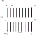
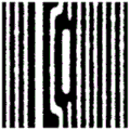
Referring to fig. 1, a first pattern 100 to be imaged by an imaging system is shown, and a resulting image 110 of the pattern 100. Due to system scanning and sample time non-linearity, the image 110 has non-uniform vertical line spacing due to imperfections associated with scanning imaging systems. As shown by features 111 and 101, the vertical line displacement is 0 at the beginning and also 0 at the end of the image, as shown by features 102 and 112. The deviation between the actual position of the feature, which is known from the pattern 100, and the image characteristic 110 can be used to determine a distortion curve. The distortion curve may be used to determine a distortion correction factor based on the expected position.
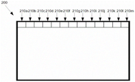
Referring to fig. 2, a first row of pixels of a given image 200 is shown. In some scanning imaging systems, image-related data is sampled at a given rate as the beam illumination point passes over the substrate; each sample is used to generate pixel values 210a to 210 m. Distortion occurs due to non-linearity between the sampling rate and the scan rate. To provide an illustrative example, the same imaging system, operating under the same operating characteristics, will be assumed to generate the image 110 of the substrate with the known pattern 100 shown in FIG. 1. By comparing the image 110 to the substrate having known characteristics 100, a distortion curve may be generated. As an example shown in fig. 3, a distortion curve is generated in the form of a graph, which represents this contrast. The distortion curve 310 in the distortion graph 300 shows the degree of pixel shift applied at the edge of each pixel of the pixel row shown in fig. 2, as shown in fig. 4. Fig. 5 shows the results of this application, along with the actual locations of the data acquisitions 510a through 510 m. The position correction samples 510a to 510m represent the positions of distortion corrected image-related data collected therefrom. However, since the pixel size is actually fixed in the resulting image, the acquired sample must be corrected to a fixed image pixel. This is achieved by calculating a corrected pixel image value based on the amount by which each sample overlaps a fixed pixel in proportion to the position corrected acquired image correlation value. For a row of pixels that only considers a single dimension, the following exemplary equation may be used to determine the correction value for a pixel:

where i is a fixed pixel index in the pixel row; corrPx [ i ] is the corrected image correlation value for the i-th fixed pixel in the pixel row; j is an index of each position correction sample, and an index of a portion of each position correction sample superimposed on the fixed pixel; n is the total number of position correction samples and the portion of the position correction samples that overlap on the ith fixed pixel value; px [ j ] is an image correlation value of each position correction sample, or an image correlation value of a portion of the position correction sample superimposed on a fixed pixel; [j] length is the length of each position correction sample, or the length of the position correction sample superimposed on a fixed pixel; and corr [ i ]. length is the length of the ith fixed pixel. As a clarifying example, if only a portion of the position correction samples overlap on a fixed pixel, then the contribution of the corrected image correlation value will thus be the sampled image correlation value multiplied by the fraction of the fixed pixel length (rather than the entire length of the position correction samples) only on the overlapping portion of the position correction samples.
Although fig. 1-5 show embodiments associated with a row of pixels, or distortion correction across one dimension, such as the width of the imaging region, the same principles can be applied in two dimensions and three dimensions. A distortion curve may be generated to correct for distortion across the length and width of an image region to account for differences between the expected and actual positions of samples at all regions of the sample. For some applications and systems, distortion correction across width only provides sufficient correction at a particular resolution. In other cases, distortion correction across length and width may be required. The above formula will be modified to the following 2D formula:

the values are the same as described above. j is still the index of each position correction sample and the index of the part of each position correction sample that overlaps on the fixed pixel, except in this case the proportion of each image correlation value is based on the overlapping area of each position correction sample or part thereof, where the image correlation value is used in correcting the image correlation value. With respect to three dimensions, a different two-dimensional distortion curve may be generated for each cross-section of the substrate, or a complete three-dimensional representation of the distortion curve may be generated over the entire volume of the substrate. In the former case, the 2D formula may be applied on each layer using a different 2D distortion curve for 3421 for each layer. Alternatively, for a fixed 3D pixel volume, a complete 3D distortion curve may be generated within the fixed 3D pixel, in which the above formula is calculated from the proportion of the volume of the correction sample or a partial volume thereof for each position. When layer removal is not possible or desirable and the imaging method does not require such removal, the 3D distortion curve and applicable distortion correction will be used for cross-sectional analysis.
In one embodiment, an imaging device for imaging a substrate is provided, the device comprising a beam emitter for directing emission at a desired location on the substrate so as to generate a detectable signal representative of the substrate. The beam transmitter may be an integral part of the apparatus, both of which may generate and direct a beam of a particular beam composition having a definable operating characteristic (e.g., composition, intensity, etc.). In other cases, the beam emitter may allow or direct ambient light or other electromagnetic radiation toward the substrate. The light beam may include the following non-limiting examples: light, electrons, ions, X-rays, magnetic energy, electromagnetic energy. In other words, the imaging system may be an optical imaging system, or it may irradiate the sample with different types of particles (e.g. X-rays, ions, etc.), or it may irradiate the sample with various forms of electromagnetic radiation or energy (e.g. X-rays, electromagnetic waves, etc.). The emission from the beam emitter causes the substrate to generate a detectable signal that is associated with a particular location thereon. The detectable signal may comprise a scattered or reflected beam of light emitted, or it may contain secondary electrons or other excitations. Either way, the emitted illumination causes a detectable signal originating from a particular location on or in the substrate.
In some embodiments, the desired location on the substrate is located on an outer surface of the substrate. Detectable signals may be acquired or measured for a plurality of desired locations on the substrate in order to characterize the surface of the substrate for the purpose of generating an image. In some embodiments, the desired location is on an interior cross-section of the substrate; in this case, the detectable signal may be collected along a location at a cross-section of the material, or along an internal feature. In some cases, multiple cross-sections are imaged and aligned to develop a 3D model of the substrate. Alternatively, the 3D model or image may be vertically aligned by imaging the substrate surface, removing the layer from the substrate, imaging the exposed surface, and repeating these steps; the resulting images may then be vertically aligned. The latter method results in repeated stripping layers, and therefore, in most cases, the substrate is damaged.
The device further comprises a signal detector for detecting an imaging characteristic of said detectable signal. In the following embodiments, the detected imaging characteristic of the detectable signal is typically correlated to the detected intensity of the signal. However, those skilled in the art will appreciate that different signal characteristics may be measured and/or quantified, alone or in combination, to image a particular substrate, such as signal wavelength, color, frequency, phase, spectrum, intensity, etc., without departing from the general scope and nature of the disclosed invention.
In some embodiments, the detectable signal may be a reflection or backscattering of an emission output from the beam emitter (e.g., electrons in a Scanning Electron Microscope (SEM), ions in a focused ion beam device (FIB), or light in an optical system). In other cases, the detectable signal is an emission through the sample (e.g., a TEM). In other cases, once the illumination is emitted, secondary particles, such as electrons or ionized particles, are generated and the signal detector may measure or detect the intensity associated therewith. In other cases, the emissions may cause other types of excitation (and resulting relaxation) that may be detected by the signal detector and associated with the desired location.
The imaging device is configured to automatically correlate the intensity with a corrected substrate position for generating a distortion corrected image, wherein the corrected substrate position is determined by the expected position and a correction factor. The correction factor is a function of the expected position. For any given system, the correction factor is predetermined based on the expected position when at least one operating characteristic is maintained at a constant value. For example, the beam of light passes through or is directed at a substrate having known surface characteristics while the chamber pressure, temperature, and ambient gas are held constant and the beam intensity and composition are held at constant levels. The resulting image is compared to the known surface features to generate a correction factor for each sampling location. While most systems attempt to minimize any error between the expected and actual locations of the sample (which includes the size of the sample region), and indeed many systems also attempt to compensate for any such error, the disclosed invention uses empirical data for an imaging system that has at least one constant operating characteristic to generate a correction factor at each expected location on the substrate based on this location. Thus, the complexity and interaction between all sources of error, and the offset, becomes insignificant, since each system under a given operating condition can be characterized, and such characterization can be applied in all future uses under such operating conditions to correct distortion. The correction factors can then be used to determine the actual size and position to which the detected signals are related, after which any distortion correction can be made to the resulting image, no matter how complex the cause of the distortion is.
In some embodiments, the system is a scanning imaging system that uses one or a combination of a beam emitter actuator, a substrate actuator, or a signal detector to measure signal strengths associated with different expected locations on the substrate. In some embodiments, for example using SEM and/or FIB, electromagnetic coils can be used to change the shape and direction of the emitted radiation by changing the potential drop around such coils to sweep the beam across the substrate. In some embodiments, the mechanical actuator may change the orientation and position of the beam transmitter itself. In both cases, the substrate and the signal detector remain stationary. In other cases, the emitted light beams remain in the same orientation and direction while either or both of the substrate and/or the signal detector are moved. In some cases, combinations of these components may be moved or remain unchanged. In any case, a signal associated with a particular location on the substrate should be associated with a given signal strength measurement. For a scanning imaging device, the beam passes through the substrate in a predetermined path, and the sample is measured at a predetermined rate. As with other types of devices, the sampling rate need not be closely related, as the device may acquire samples at predetermined expected locations and then use the intensity levels and expected locations (corrected for distortion) in the generated image data.
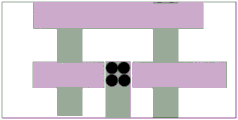
In some embodiments, multiple samples of signal intensity values are used to generate image pixels, where each sample of signal intensity values is associated with an actual location on or within the substrate. Since the actual position of the substrate is not necessarily aligned with the pixels of the image, they should be corrected. In some embodiments, this is accomplished by associating each pixel with a corrected intensity value that the pixel uses to fill in pixel image values to the pixel, which in turn can be used to determine the color or grayscale value of the pixel. There are image pixel values and image pixels corresponding to each expected substrate location, and the image pixel values are based on respective proportions of at least one signal intensity value whose corrected substrate location corresponds to a portion of the image pixels. The corrected intensity value for each pixel image value is determined with a proportion of each intensity value associated with the corrected location corresponding to that pixel location, the proportion being equal to the proportion of the size of the corrected location of the pixel size. For example, if a pixel location corresponds to the same location as a given correction location (or indeed if the location of the correction is greater than the pixel), then the corrected intensity value for that pixel is the same as the intensity measurement originating from that correction location. Referring to FIG. 6, an exemplary determination is illustrated. In the row corresponding to a fixed image pixel 600, the intensity of C1, otherwise known as p [ C1], is equivalent to the proportion of all samples 610 having a corrected position corresponding to C1. In this case, C1 corresponds exactly to A1, so p [ C1] equals p [ A1 ]. Only a6 contributes to C6, so p [ C6] ═ p [ a6 ]. C5 corresponds to portions a5 and a 6; accordingly, p [ C6] ═ p [ a6], 65% of C5 from a portion of a5 and 35% from a portion of a6, so p [ C5] ═ 0.65p [ a5] +0.35p [ a6 ]. In general, this contribution will be related to the detected intensity values associated with the actual location detection, although other embodiments may use other formulas and methods for determining pixel image values. The actual position detection corresponds to some or all of the pixel image values corresponding to the same position on the substrate.
In some embodiments, the apparatus comprises, in an integrated manner, the beam emitter, the substrate table and the signal detector. In other cases, the apparatus comprises a system in which each of the components is held in a non-integral part. The associating, measuring, determining, and correcting steps may be carried out by a communicatively coupled computing device, which may be integrally associated with the apparatus, or alternatively, as a system that is not integral to the device or system. As will be appreciated by those skilled in the art, the computing device may include different combinations of processing, communication, and data storage and memory components.
In some embodiments, a method of correcting image distortion in an imaging device or imaging system is provided. The imaging device or system comprises a beam emitter for directing emission at the substrate to produce a detectable signal representative of the associated substrate at the desired location, and a signal detector for determining an intensity value of said detectable signal. The method comprises the following steps: the emission is caused to illuminate the substrate so as to produce a detectable signal that is correlated with an expected location, which typically corresponds to an image pixel location on the area of the substrate being imaged. This detectable signal may be a reflected, scattered or non-absorbed portion of the emission from the beam emitter, or it may be a secondary signal caused by the emission illumination. Measuring, by the signal detector, an intensity of the detectable signal, the intensity initially associated with the measured expected location; the corrected substrate position is associated with a measured intensity associated with a corrected substrate position for generating a distortion corrected image, wherein the corrected substrate position is calculated from the expected position and a correction factor that is a function of the expected substrate position. Once sufficient intensity values are measured from a portion of the substrate to provide image data for an area of the substrate (on its surface or its cross-section), a corrected intensity value for each image pixel is determined by correlating a proportional amount of all corrected substrate locations corresponding to the pixel location in the imaged area.
In some embodiments, a method of determining a correction factor for a given imaging system at one or more constant operating characteristics is provided. The method involves imaging or detecting signal intensities associated with surface features on a substrate having known surface features and then comparing the resulting image with the known surface features (or signal intensity values associated with measured expected locations, as the case may be). Based on the difference, the translation in one or more directions (or dimensions, i.e., length, width, or depth) may be determined based on the expected location. At each desired location in a given substrate, the correction factor is expressed as a transformation or vector having a direction, and may also be expressed as one or more distortion curves or distortion indices. The correction factor can then be used to account for distortion correction for substrates imaged in the same device under the same operating conditions.
An exemplary set of imaging results from one embodiment is described, including the resulting distortion-corrected images and corresponding uncorrected images of the same substrate, as shown in fig. 11-16. This embodiment of the distortion-corrected imaging system comprises a first scanning electron microscope (SEM-a), a second scanning electron microscope (SEM-B), a high resolution image capture system, a calibration sample (comprising a substrate with a series of known gridlines of nanometer precision, the characteristics of which are detectable by the capture system), an integrated circuit sample, an associated daA processing device (e.g., computer) for running various software applications, including software for applying distortion correction processing to individual images, image stitching software, mosaicking overlay and navigation software.
An exemplary embodiment of one of the methods of correcting imaging distortion in the above system comprises the following steps. Using SEM-A and SEM-B, a series of SEM images were taken from the calibration sample under different operating conditions. Exemplary operating conditions may include: fixed working distance (8 mm), fixed pixel dwell time (0.20 microseconds per pixel), fixed aperture (60 microns), fixed detector signal amplification range (high), fixed pixel resolution (16000x 16000), acceleration voltage (8 kv, 9kv, 10 kv), field of view FOV (50 microns, 75 microns, 100 microns, 150 microns). By comparing the resulting image of each permutation combination of the above parameters with known characteristics of the calibration sample, the relationship of each set of operating conditions can be determined in terms of expected positions (which may include dimensions and the position of the resulting capture position, since the size of the area of the substrate on which the beam is incident will vary from one expected position to another). A correction function may be developed in which the size and position of the actual area and the image capture location may be returned for a given input of expected location when image data is captured for the imaging device under a given set of operating parameters.
Finally, many parameters may be varied and data collected to give a complete working range for characterizing distortion at any given location within the FOV. It should be noted that not all parameters will affect the distortion to the same extent, and some simplified parameters may be utilized depending on the equipment used. Experimental design methods may be used to reduce the number of tests. Each particular SEM (even from the same vendor) may have a different sensitivity and the correct algorithm may be employed only by measuring the range of the parameter space and making a decision based on the final accuracy required. In the present embodiment, single-pixel accuracy is required.
Once the correction function is established, the unknown sample (partially delayed IC) can be imaged using the most appropriate parameters (parameter values shown in the table below) to give image set # 1. The most fundamental requirement is the fastest imaging (maximum FOV) while still having sufficient resolution to identify the smallest circuit elements. The following table shows the imaging parameters for each image set.
| Parameter(s) | Parameter values of image set #1 | Parameter values of image set #2 |
| SEM | SEM-A | SEM-B |
| Imaging region | 1200x 1600 microns | 1200x 1650 |
| FOV | ||
| 100 micron | 75 micron | |
| Imaging stitching | 12x 16 image | 16x 22 image |
| Number of images | 192 | 352 |
| Pixel of each image | 16,000x 16,000 | 16,000x 16,000 |
| SEM kilovolt | 10 kilovolt | 8 kilovolt |
| SEM hole | 60 micron | 60 micron |
| SEM detector gain | Height of | Height of |
After image acquisition of the entire layer, the partially delayed IC is further partially delayed to show the circuitry of the next layer, and the imaging step is repeated but with different parameters (to match the newly exposed circuit layer with smaller circuit elements) and different SEMs. This creates image set #2 which is stitched together to form the entire imaged layer 1100, as shown in FIG. 11. The alignment lines for each stitched image, as at 1110, are shown in FIG. 11. Fig. 12 shows one single image of the image set # 2.
A distortion correction algorithm suitable for each SEM and each set of parameter values is applied to each individual image from both data sets. After correction, the images are stitched, aligned and arranged into a mosaic. Fig. 13 shows two enlarged regions of one image in the image set # 1. Fig. 13a is taken near the left edge of the image and fig. 13b is taken near the center. FIGS. 14a and 14b show two magnified regions of an image in image set # 2; fig. 14a shows an image from the vicinity of the edge of the image set #2, and fig. 14b shows an image from the vicinity of the center of the image set # 2. In fig. 15a and 15b, two magnified regions from one image in the correction image set #1 are shown at the top of the magnified region of response from one image in the correction image set # 2. Fig. 15a and 15b show perfect vertical alignment, where the interconnect vias of image set #2 are precisely aligned with the metal lines in image set # 1. This is true near the edges and near the center of the image. In contrast, fig. 16a and 16b show the same area, but the image is not corrected. Misalignment near the center of the image is apparent when the magnified area is well aligned at the edge of the image.
While the present invention has been described in terms of various exemplary embodiments, it is not intended that the invention be limited to the disclosed embodiments. On the contrary, the invention is intended to cover various modifications and equivalent arrangements included within the scope of the appended claims.
Claims (16)
1. An imaging device for imaging at least a portion of at least one layer in a substrate, the device comprising:
a beam emitter for directing emission toward the guide substrate so as to produce detectable signals representative of said portion of the substrate at a plurality of desired locations on the substrate; and
a signal detector for detecting an imaged feature of said detectable signal for each of said desired locations;
one or more actuators for changing the position of the emission relative to the substrate to detect the imaged feature at each of the expected locations of the substrate;
wherein the imaging device automatically associates the imaging features with a preset image resolution and a corrected substrate position at each of the expected locations for generating a distortion corrected image, wherein the corrected substrate position is determined from the expected locations and a correction factor, wherein the correction factor is a function of the expected locations and the preset image resolution, the preset image resolution corresponding to the expected locations;
wherein the imaging device is configured to align a plurality of the distortion corrected images to form a mosaic image of the portion of at least one layer in the substrate, the distortion corrected images comprising at least two different image resolutions.
2. The device of claim 1, wherein the imaging characteristic comprises an intensity of the detectable signal.
3. The apparatus of claim 1, wherein the correction factor is predetermined for at least one operating characteristic of the imaging apparatus.
4. A device according to any one of claims 1 to 3, wherein the actuator is a beam actuator for changing the direction of emission relative to the substrate position to detect the imaged feature at one or more different desired locations.
5. A device according to any one of claims 1 to 3 wherein the actuator is a device actuator for changing the position of the signal detector and thereby the relative position of the signal detector and the substrate to detect the imaged feature at one or more different desired locations.
6. An apparatus according to any one of claims 1 to 3 wherein the actuator is a substrate actuator for changing the position of the substrate such that the substrate remains in correspondence with the beam emitter and the signal detector.
7. The apparatus of any one of claims 1 to 3, wherein the signal detector determines a corresponding feature for each of a plurality of different corresponding expected positions, and wherein the imaging device automatically associates each of the corresponding features with a respective corrected substrate position for use in generating the distortion corrected image.
8. The apparatus of any of claims 1 to 3, wherein the given image pixel value for the given image pixel location corresponding to the given expected location is based on a respective proportion of the imaging feature associated with any of the at least one or more of the corrected substrate locations that at least partially overlap the given image pixel location.
9. The device according to any one of claims 1 to 3, wherein the device is selected from the group consisting of: optical imaging devices, FIB, SEM, TEM, X-ray devices, MRI, ion beam devices, CT scans and CAT scans.
10. The apparatus of claim 3, wherein the at least one operating characteristic comprises a current imaging resolution of the apparatus.
11. A method of correcting image distortion in an imaging device comprising a beam emitter for directing emission at a substrate to generate a detectable signal indicative of said substrate at a desired location, and a signal detector for determining an imaging characteristic representative of said detectable signal, the method comprising:
illuminating the emission onto the substrate;
measuring an imaging characteristic of the detectable signal associated with the expected location and a location-dependent image resolution;
determining a corrected substrate position associated with an imaging feature used to generate a distortion corrected image, the corrected substrate position determined from the expected position and a specified correction factor, the specified correction factor predetermined as a function of the expected position, the distortion corrected image having an image resolution associated with the corrected substrate position;
correlating the imaged feature of the measured detectable signal with the corrected substrate position;
repeating the measuring, determining and correlating steps for at least one other expected location; and
aligning a plurality of the distortion corrected images to form a mosaic image of portions of at least one layer in the substrate, the distortion corrected images comprising at least two different image resolutions.
12. The method of claim 11, wherein the imaging characteristic comprises an intensity of the detectable signal.
13. The method of claim 11, wherein the correction factor is further predetermined for a set of operating characteristics of the imaging device.
14. The method of any of claims 11 to 13, further comprising a given image pixel value having a given image pixel location corresponding to an expected location on the substrate, the given image pixel value being based on a respective scale of the imaging feature, the imaging feature being associated with one or more of the corrected substrate locations, and the corrected substrate locations overlapping at least a portion of the given image pixel location.
15. A method of generating an image of a substrate from an imaging device, the imaging device comprising a beam source for directing emissions to predetermined locations on a substrate to obtain an image resolution associated with the predetermined locations, and a signal detector for determining a signal feature value associated with the emissions, the method comprising:
collecting a plurality of signal feature values with the signal detector, each of the signal feature values representing a characteristic of the substrate at an actual location;
determining for each given signal characteristic value an actual position associated therewith by correcting the predetermined position with a correction factor; and are
Generating image pixel values for the image, wherein a given image pixel value at a given image pixel location is based on the position-dependent image resolution and a corresponding ratio of at least one of the given signal feature values whose corrected substrate position corresponds to a portion of the given image pixel location;
generating an image from a plurality of said image pixel values, said image pixel values comprising at least two different said position dependent image resolutions.
16. The method of claim 15, wherein the correction factor is associated with at least one operational characteristic of the imaging device.
Applications Claiming Priority (3)
| Application Number | Priority Date | Filing Date | Title |
|---|---|---|---|
| US201562137078P | 2015-03-23 | 2015-03-23 | |
| US62/137,078 | 2015-03-23 | ||
| PCT/CA2016/050328 WO2016149817A1 (en) | 2015-03-23 | 2016-03-22 | Methods, systems and devices relating to distortion correction in imaging devices |
Publications (2)
| Publication Number | Publication Date |
|---|---|
| CN107533017A CN107533017A (en) | 2018-01-02 |
| CN107533017B true CN107533017B (en) | 2021-01-08 |
Family
ID=56976889
Family Applications (1)
| Application Number | Title | Priority Date | Filing Date |
|---|---|---|---|
| CN201680023239.8A Active CN107533017B (en) | 2015-03-23 | 2016-03-22 | Method, system and apparatus relating to distortion correction in an imaging device |
Country Status (6)
| Country | Link |
|---|---|
| US (1) | US10469777B2 (en) |
| EP (2) | EP4009042A1 (en) |
| JP (1) | JP7294806B2 (en) |
| CN (1) | CN107533017B (en) |
| CA (1) | CA2980201C (en) |
| WO (1) | WO2016149817A1 (en) |
Families Citing this family (11)
| Publication number | Priority date | Publication date | Assignee | Title |
|---|---|---|---|---|
| WO2013173728A1 (en) | 2012-05-17 | 2013-11-21 | The University Of North Carolina At Chapel Hill | Methods, systems, and computer readable media for unified scene acquisition and pose tracking in a wearable display |
| WO2016073557A1 (en) | 2014-11-04 | 2016-05-12 | The University Of North Carolina At Chapel Hill | Minimal-latency tracking and display for matching real and virtual worlds |
| JP6867015B2 (en) * | 2017-03-27 | 2021-04-28 | 株式会社日立ハイテクサイエンス | Automatic processing equipment |
| GB201715902D0 (en) * | 2017-09-29 | 2017-11-15 | Oxford Instr Plc | Improved system for electron diffraction analysis |
| CA3081760A1 (en) | 2017-11-15 | 2019-05-23 | Butterfly Network, Inc. | Ultrasound apparatuses and methods for fabricating ultrasound devices |
| JP6934811B2 (en) * | 2017-11-16 | 2021-09-15 | 株式会社ミツトヨ | Three-dimensional measuring device |
| DE102018204683B3 (en) * | 2018-03-27 | 2019-08-08 | Carl Zeiss Microscopy Gmbh | electron microscope |
| US10410372B1 (en) * | 2018-06-14 | 2019-09-10 | The University Of North Carolina At Chapel Hill | Methods, systems, and computer-readable media for utilizing radial distortion to estimate a pose configuration |
| FR3087928B1 (en) | 2018-10-29 | 2020-11-06 | Texplained | PROCESS FOR PROCESSING A PLURALITY OF ELEMENTARY IMAGES ACQUIRED ON AN INTEGRATED CIRCUIT |
| US10834306B2 (en) * | 2019-01-15 | 2020-11-10 | International Business Machines Corporation | Method for a remote control of a radiation detection apparatus |
| KR102608797B1 (en) * | 2023-04-10 | 2023-12-01 | 부산대학교 산학협력단 | Apparatus and Method for Correcting Geometric Distortions in X-ray Backscatter Imaging |
Citations (5)
| Publication number | Priority date | Publication date | Assignee | Title |
|---|---|---|---|---|
| EP0370322A2 (en) * | 1988-11-23 | 1990-05-30 | Schlumberger Technologies, Inc. | Method and apparatus for alignment of images |
| JP2000149853A (en) * | 1998-11-06 | 2000-05-30 | Nikon Corp | Observation device and adjustment thereof |
| EP1455378A1 (en) * | 2001-11-21 | 2004-09-08 | Hitachi High-Technologies Corporation | Sample imaging method and charged particle beam system |
| CN101371326A (en) * | 2005-12-02 | 2009-02-18 | 阿利斯公司 | Ion sources, systems and methods |
| WO2011089911A1 (en) * | 2010-01-25 | 2011-07-28 | 株式会社日立ハイテクノロジーズ | Charged particle beam microscope and method of measurement employing same |
Family Cites Families (27)
| Publication number | Priority date | Publication date | Assignee | Title |
|---|---|---|---|---|
| CA2216900C (en) * | 1996-10-01 | 2001-12-04 | Semiconductor Insights Inc. | Method to extract circuit information |
| JP4002655B2 (en) | 1998-01-06 | 2007-11-07 | 株式会社日立製作所 | Pattern inspection method and apparatus |
| US7817844B2 (en) * | 1999-08-26 | 2010-10-19 | Nanogeometry Research Inc. | Pattern inspection apparatus and method |
| US20030003600A1 (en) * | 2001-07-02 | 2003-01-02 | Fuji Photo Film Co., Ltd. | Biochemical analysis kit and method for exposing stimulable phosphor sheet |
| DE10332059A1 (en) | 2003-07-11 | 2005-01-27 | Carl Zeiss Sms Gmbh | Analysis of microlithography objects, especially masks using aerial image measurement systems, whereby a detected image is corrected using a transfer function correction filter |
| US7313781B2 (en) | 2004-05-28 | 2007-12-25 | Kabushiki Kaisha Toshiba | Image data correction method, lithography simulation method, image data correction system, program, mask and method of manufacturing a semiconductor device |
| WO2007024221A1 (en) | 2005-08-23 | 2007-03-01 | University Of Washington | Distance determination in a scanned beam image capture device |
| WO2007067296A2 (en) | 2005-12-02 | 2007-06-14 | Alis Corporation | Ion sources, systems and methods |
| DE102005062618B4 (en) | 2005-12-23 | 2008-05-08 | Carl Zeiss Smt Ag | Optical imaging device and imaging method with determination of aberrations |
| JP4979246B2 (en) * | 2006-03-03 | 2012-07-18 | 株式会社日立ハイテクノロジーズ | Defect observation method and apparatus |
| JP4801518B2 (en) * | 2006-07-07 | 2011-10-26 | 株式会社日立ハイテクノロジーズ | Charged particle beam microscopic method and charged particle beam apparatus |
| JP2008046470A (en) * | 2006-08-18 | 2008-02-28 | Olympus Corp | Illumination device, illumination method, and scanning type optical microscope |
| JP5134804B2 (en) * | 2006-10-06 | 2013-01-30 | 株式会社日立ハイテクノロジーズ | Distortion calibration of scanning electron microscope and scanning electron microscope images |
| US20110304527A1 (en) * | 2007-09-14 | 2011-12-15 | Sean Wu | Computer-implemented methods, carrier media, and systems for displaying an image of at least a portion of a wafer |
| JP4856047B2 (en) * | 2007-11-12 | 2012-01-18 | 株式会社東芝 | Mask pattern dimension inspection method and mask pattern dimension inspection apparatus |
| US8326011B2 (en) * | 2008-05-21 | 2012-12-04 | Varian Medical Systems, Inc. | Methods, systems, and computer-program products for estimating scattered radiation in radiographic projections |
| JP2010002772A (en) * | 2008-06-20 | 2010-01-07 | Toshiba Corp | Pattern verification-inspection method, method for acquiring distribution of optical image intensity, and program for acquiring distribution of optical image intensity |
| EP2197018A1 (en) * | 2008-12-12 | 2010-06-16 | FEI Company | Method for determining distortions in a particle-optical apparatus |
| JP5472690B2 (en) * | 2009-06-23 | 2014-04-16 | 株式会社島津製作所 | Scanning beam irradiation device |
| JP5547942B2 (en) * | 2009-10-06 | 2014-07-16 | 株式会社日立ハイテクノロジーズ | Defect observation method and apparatus |
| US8253118B2 (en) | 2009-10-14 | 2012-08-28 | Fei Company | Charged particle beam system having multiple user-selectable operating modes |
| JP5357725B2 (en) * | 2009-12-03 | 2013-12-04 | 株式会社日立ハイテクノロジーズ | Defect inspection method and defect inspection apparatus |
| JP5963453B2 (en) * | 2011-03-15 | 2016-08-03 | 株式会社荏原製作所 | Inspection device |
| JP5651511B2 (en) * | 2011-03-22 | 2015-01-14 | 株式会社東芝 | Photomask pattern contour extraction method and contour extraction device |
| CA2835713C (en) | 2011-05-13 | 2023-04-04 | Fibics Incorporated | Microscopy imaging method and system |
| JP5809575B2 (en) * | 2012-01-31 | 2015-11-11 | 株式会社日立ハイテクノロジーズ | Image processing apparatus and method, distortion correction map creating apparatus and method, and semiconductor measurement apparatus |
| EP3155361A2 (en) | 2014-06-10 | 2017-04-19 | Carl Zeiss Meditec, Inc. | Improved frequency-domain interferometric based imaging systems and methods |
-
2016
- 2016-03-22 CA CA2980201A patent/CA2980201C/en active Active
- 2016-03-22 US US15/560,935 patent/US10469777B2/en active Active
- 2016-03-22 EP EP21215776.2A patent/EP4009042A1/en active Pending
- 2016-03-22 CN CN201680023239.8A patent/CN107533017B/en active Active
- 2016-03-22 JP JP2018500832A patent/JP7294806B2/en active Active
- 2016-03-22 EP EP16767584.2A patent/EP3274698A4/en not_active Withdrawn
- 2016-03-22 WO PCT/CA2016/050328 patent/WO2016149817A1/en active Application Filing
Patent Citations (5)
| Publication number | Priority date | Publication date | Assignee | Title |
|---|---|---|---|---|
| EP0370322A2 (en) * | 1988-11-23 | 1990-05-30 | Schlumberger Technologies, Inc. | Method and apparatus for alignment of images |
| JP2000149853A (en) * | 1998-11-06 | 2000-05-30 | Nikon Corp | Observation device and adjustment thereof |
| EP1455378A1 (en) * | 2001-11-21 | 2004-09-08 | Hitachi High-Technologies Corporation | Sample imaging method and charged particle beam system |
| CN101371326A (en) * | 2005-12-02 | 2009-02-18 | 阿利斯公司 | Ion sources, systems and methods |
| WO2011089911A1 (en) * | 2010-01-25 | 2011-07-28 | 株式会社日立ハイテクノロジーズ | Charged particle beam microscope and method of measurement employing same |
Also Published As
| Publication number | Publication date |
|---|---|
| CN107533017A (en) | 2018-01-02 |
| CA2980201A1 (en) | 2016-09-29 |
| EP4009042A1 (en) | 2022-06-08 |
| US20180054575A1 (en) | 2018-02-22 |
| CA2980201C (en) | 2023-06-27 |
| US10469777B2 (en) | 2019-11-05 |
| WO2016149817A1 (en) | 2016-09-29 |
| EP3274698A4 (en) | 2018-12-26 |
| JP7294806B2 (en) | 2023-06-20 |
| EP3274698A1 (en) | 2018-01-31 |
| JP2018517146A (en) | 2018-06-28 |
Similar Documents
| Publication | Publication Date | Title |
|---|---|---|
| CN107533017B (en) | Method, system and apparatus relating to distortion correction in an imaging device | |
| JP5156619B2 (en) | Sample size inspection / measurement method and sample size inspection / measurement device | |
| JP4801518B2 (en) | Charged particle beam microscopic method and charged particle beam apparatus | |
| JP5202071B2 (en) | Charged particle microscope apparatus and image processing method using the same | |
| KR100310106B1 (en) | Pattern inspection method and device | |
| KR100721846B1 (en) | Patterned wafer inspection method and apparatus therefor | |
| KR101101463B1 (en) | Scanning electron microscope having length measuring function and sample dimension length measuring method | |
| US20060284088A1 (en) | Focus correction method for inspection of circuit patterns | |
| US7526143B2 (en) | Imaging method | |
| US8330104B2 (en) | Pattern measurement apparatus and pattern measurement method | |
| US20030006371A1 (en) | Charged-particle beam apparatus and method for automatically correcting astigmatism of charged-particle beam apparatus | |
| JP4974737B2 (en) | Charged particle system | |
| US11170969B2 (en) | Electron beam observation device, electron beam observation system, and control method of electron beam observation device | |
| WO2013015040A1 (en) | Charged particle beam apparatus and measuring method | |
| JPH1140096A (en) | Particle bew inspection system and inspection method, and particle bew-applyed system | |
| KR102477184B1 (en) | Method for inspecting a sample with a charged particle beam device, and charged particle beam device | |
| JP4186464B2 (en) | Charged particle beam scanning system | |
| JP4028864B2 (en) | Pattern defect inspection method and inspection apparatus | |
| JP3950891B2 (en) | Pattern defect inspection method and pattern defect inspection apparatus | |
| KR20230041806A (en) | How to Image a Sample with a Charged Particle Beam Device, How to Calibrate a Charged Particle Beam Device, and a Charged Particle Beam Device | |
| CN113228222A (en) | Method for calibrating a scanning charged particle microscope | |
| JP2009211961A (en) | Scanning electron microscope | |
| JP2017084631A (en) | Image correction device | |
| JPH11237230A (en) | Method and equipment for specimen measuring in electron microscope | |
| KR20220131852A (en) | Image generation for examination of a semiconductor specimen |
Legal Events
| Date | Code | Title | Description |
|---|---|---|---|
| PB01 | Publication | ||
| PB01 | Publication | ||
| SE01 | Entry into force of request for substantive examination | ||
| SE01 | Entry into force of request for substantive examination | ||
| GR01 | Patent grant | ||
| GR01 | Patent grant |