JP5638396B2 - System and method for material analysis of fine elements - Google Patents
System and method for material analysis of fine elements Download PDFInfo
- Publication number
- JP5638396B2 JP5638396B2 JP2010543626A JP2010543626A JP5638396B2 JP 5638396 B2 JP5638396 B2 JP 5638396B2 JP 2010543626 A JP2010543626 A JP 2010543626A JP 2010543626 A JP2010543626 A JP 2010543626A JP 5638396 B2 JP5638396 B2 JP 5638396B2
- Authority
- JP
- Japan
- Prior art keywords
- charged particle
- particle beam
- mode illumination
- area
- during
- Prior art date
- Legal status (The legal status is an assumption and is not a legal conclusion. Google has not performed a legal analysis and makes no representation as to the accuracy of the status listed.)
- Expired - Fee Related
Links
Images


Classifications
-
- H—ELECTRICITY
- H01—ELECTRIC ELEMENTS
- H01J—ELECTRIC DISCHARGE TUBES OR DISCHARGE LAMPS
- H01J37/00—Discharge tubes with provision for introducing objects or material to be exposed to the discharge, e.g. for the purpose of examination or processing thereof
- H01J37/26—Electron or ion microscopes; Electron or ion diffraction tubes
- H01J37/28—Electron or ion microscopes; Electron or ion diffraction tubes with scanning beams
-
- H—ELECTRICITY
- H01—ELECTRIC ELEMENTS
- H01J—ELECTRIC DISCHARGE TUBES OR DISCHARGE LAMPS
- H01J37/00—Discharge tubes with provision for introducing objects or material to be exposed to the discharge, e.g. for the purpose of examination or processing thereof
- H01J37/02—Details
- H01J37/22—Optical or photographic arrangements associated with the tube
- H01J37/222—Image processing arrangements associated with the tube
-
- H—ELECTRICITY
- H01—ELECTRIC ELEMENTS
- H01J—ELECTRIC DISCHARGE TUBES OR DISCHARGE LAMPS
- H01J37/00—Discharge tubes with provision for introducing objects or material to be exposed to the discharge, e.g. for the purpose of examination or processing thereof
- H01J37/02—Details
- H01J37/244—Detectors; Associated components or circuits therefor
-
- H—ELECTRICITY
- H01—ELECTRIC ELEMENTS
- H01J—ELECTRIC DISCHARGE TUBES OR DISCHARGE LAMPS
- H01J37/00—Discharge tubes with provision for introducing objects or material to be exposed to the discharge, e.g. for the purpose of examination or processing thereof
- H01J37/26—Electron or ion microscopes; Electron or ion diffraction tubes
- H01J37/261—Details
- H01J37/263—Contrast, resolution or power of penetration
-
- H—ELECTRICITY
- H01—ELECTRIC ELEMENTS
- H01J—ELECTRIC DISCHARGE TUBES OR DISCHARGE LAMPS
- H01J37/00—Discharge tubes with provision for introducing objects or material to be exposed to the discharge, e.g. for the purpose of examination or processing thereof
- H01J37/26—Electron or ion microscopes; Electron or ion diffraction tubes
- H01J37/261—Details
- H01J37/265—Controlling the tube; circuit arrangements adapted to a particular application not otherwise provided, e.g. bright-field-dark-field illumination
-
- H—ELECTRICITY
- H01—ELECTRIC ELEMENTS
- H01J—ELECTRIC DISCHARGE TUBES OR DISCHARGE LAMPS
- H01J37/00—Discharge tubes with provision for introducing objects or material to be exposed to the discharge, e.g. for the purpose of examination or processing thereof
- H01J37/30—Electron-beam or ion-beam tubes for localised treatment of objects
- H01J37/304—Controlling tubes by information coming from the objects or from the beam, e.g. correction signals
- H01J37/3045—Object or beam position registration
-
- H—ELECTRICITY
- H01—ELECTRIC ELEMENTS
- H01J—ELECTRIC DISCHARGE TUBES OR DISCHARGE LAMPS
- H01J2237/00—Discharge tubes exposing object to beam, e.g. for analysis treatment, etching, imaging
- H01J2237/245—Detection characterised by the variable being measured
- H01J2237/24571—Measurements of non-electric or non-magnetic variables
- H01J2237/24578—Spatial variables, e.g. position, distance
-
- H—ELECTRICITY
- H01—ELECTRIC ELEMENTS
- H01J—ELECTRIC DISCHARGE TUBES OR DISCHARGE LAMPS
- H01J2237/00—Discharge tubes exposing object to beam, e.g. for analysis treatment, etching, imaging
- H01J2237/25—Tubes for localised analysis using electron or ion beams
- H01J2237/2505—Tubes for localised analysis using electron or ion beams characterised by their application
- H01J2237/2511—Auger spectrometers
-
- H—ELECTRICITY
- H01—ELECTRIC ELEMENTS
- H01J—ELECTRIC DISCHARGE TUBES OR DISCHARGE LAMPS
- H01J2237/00—Discharge tubes exposing object to beam, e.g. for analysis treatment, etching, imaging
- H01J2237/25—Tubes for localised analysis using electron or ion beams
- H01J2237/2505—Tubes for localised analysis using electron or ion beams characterised by their application
- H01J2237/2555—Microprobes, i.e. particle-induced X-ray spectrometry
-
- H—ELECTRICITY
- H01—ELECTRIC ELEMENTS
- H01J—ELECTRIC DISCHARGE TUBES OR DISCHARGE LAMPS
- H01J2237/00—Discharge tubes exposing object to beam, e.g. for analysis treatment, etching, imaging
- H01J2237/30—Electron or ion beam tubes for processing objects
- H01J2237/304—Controlling tubes
- H01J2237/30455—Correction during exposure
Description
本発明は、微細要素の物質分析のための方法およびシステムに関する。 The present invention relates to a method and system for material analysis of fine elements.
集積回路は、非常に複雑な製造プロセスによって製造される。様々な製造プロセス欠陥は、集積回路上に微細要素の沈着を招く可能性がある。これらの様々な製造欠陥の解決には、これらの微細要素を形成する物質を決定することが役立つ可能性がある。 Integrated circuits are manufactured by a very complex manufacturing process. Various manufacturing process defects can lead to deposition of microelements on the integrated circuit. To resolve these various manufacturing defects, it may be helpful to determine the materials that form these microelements.
様々な物質分析法は、(電子ビームもしくはイオンビームなどの)帯電粒子ビームまたはX線ビームの焦点を対象の微細要素上に合わせる。この帯電粒子ビームは、一般に、微細要素、加えてまたは代替としては、その微細要素に隣接する試料部分を帯電させる。この帯電は、帯電粒子ビームを微細要素から偏向させることが可能である。したがって、特定の期間の後には、帯電粒子ビームは完全に、対象の要素に届かない可能性があり、物質分析は、微細要素が形成される物質を反映しなくなる。 Various material analysis methods focus a charged particle beam (such as an electron beam or ion beam) or an x-ray beam onto a fine element of interest. This charged particle beam generally charges the microelement and, in addition or alternatively, the portion of the sample adjacent to the microelement. This charging can deflect the charged particle beam from the fine elements. Thus, after a certain period of time, the charged particle beam may not completely reach the element of interest and the material analysis will not reflect the material from which the microelements are formed.
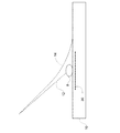
図1は、微細要素8と、経時的な帯電粒子ビームの変位とを示している。照明の開始時に、(破線12によって示される)帯電粒子ビームは、微細要素8に向かって方向付けられる。帯電粒子ビームは、(微細要素8の下の水平な破線によって示される)試料の一部分20を帯電させる。帯電した部分20は、帯電粒子ビームを変位させる電場を生成する。しばらくして、(破線14によって示される)帯電粒子ビームは、微細要素の周囲に向かって方向付けられ、微細要素8と相互作用しない。
FIG. 1 shows the
図2は、微細要素と、帯電粒子ビームの変位により、種々の時点間に走査される様々なエリアとを示している。その変位は、例えば、試料(またはその部分)の帯電から生じる。走査が開始するとき、微細要素8は、エリア30の中心に配置される。しばらくして、走査型電子顕微鏡は、別のエリア32に向かって方向付けられ、微細要素8は、このエリアに対する中心に配置されない。さらなる時間の後、微細要素8は完全に、帯電電子ビームによって走査されるエリア34の外側にある。帯電効果から生じるこの例においては、この変位が帯電粒子ビーム光学部のパラメータの意図的変更の結果でないことが分かる。
FIG. 2 shows the fine elements and the various areas that are scanned between various points in time due to the displacement of the charged particle beam. The displacement results from, for example, charging of the sample (or part thereof). When scanning starts, the
図3は、走査電子微細列に対して約45度に角度をなしたシリコンガラスのブランケットウェハ中で測定される電子ビームの変位(ドリフト)の例を示している。Y軸に沿うドリフトレートは、1秒当たり約1.4ナノメートルであり、X軸に沿うドリフトレートは、より低かった。小さい微細要素エリアが、物質分析のための電子ビームによって走査されること(例えば、30nm×30nmの微細要素内に配置される電子ビームスポット)になる場合、約10秒後に、微細要素は、電子ビームスポットの外になることが予想される。さらには、ドリフトレートは、低誘電率誘電物質から形成されたものなどの帯電した試料を走査するとき、より速くなることが予想される。 FIG. 3 shows an example of electron beam displacement (drift) measured in a silicon glass blanket wafer at an angle of about 45 degrees with respect to the scanning electron microarray. The drift rate along the Y axis was about 1.4 nanometers per second and the drift rate along the X axis was lower. If a small microelement area is to be scanned by an electron beam for material analysis (eg, an electron beam spot placed in a 30 nm × 30 nm microelement), after about 10 seconds, the microelement is It is expected to be outside the beam spot. Furthermore, the drift rate is expected to be faster when scanning charged samples such as those formed from low dielectric constant dielectric materials.
(例えば、約50nm以下の)小さい微細要素に関する物質分析のためのシステムおよび方法を提供する必要性が高まっている。 There is a growing need to provide systems and methods for material analysis on small microelements (eg, below about 50 nm).
本発明を理解するために、およびそれが実際にどのように行われることができるのかを知るために、次に、ある実施形態が、添付の図面を参照して、限定しない例によって説明されることになる。 In order to understand the present invention and to know how it can be done in practice, an embodiment will now be described by way of non-limiting example with reference to the accompanying drawings. It will be.
本発明の一実施形態によれば、微細要素の物質分析のための方法が提供され、方法は、帯電粒子ビームによって、微細要素の少なくとも一部分を含むエリアを照明し、帯電粒子ビームに応答してそのエリア内に生成される粒子を検出し、検出された粒子を分析して、微細要素の物質特性についての指標をもたらすステップを含み、照明動作は、それぞれが、連続する物質分析期間同士の間にもたらされる一連の変位補償決定期間において実施され、方法はさらに、変位補償決定期間の間に、微細要素に対する帯電粒子ビームの変位を評価し、連続する物質分析期間の間に、必要に応じて空間調整対策を適用して、それによって、帯電粒子ビームのドリフトを補償するステップを含む。 In accordance with one embodiment of the present invention, a method for material analysis of a microelement is provided, the method illuminating an area including at least a portion of the microelement with a charged particle beam and responsive to the charged particle beam. Detecting the particles produced in the area and analyzing the detected particles to provide an indication of the material properties of the microelements, each lighting operation between successive material analysis periods The method is further performed during a series of displacement compensation determination periods, and the method further evaluates the displacement of the charged particle beam relative to the microelements during the displacement compensation determination period and, if necessary, during successive material analysis periods. Applying spatial adjustment measures, thereby compensating for drift of the charged particle beam.
本発明の一実施形態によれば、微細要素に対する帯電粒子ビームの変位を評価する動作は、1つまたは複数の物質分析期間の前後に、微細要素の検出位置における変化を査定するステップを含む。 According to one embodiment of the invention, the act of evaluating the displacement of the charged particle beam relative to the microelement includes assessing changes in the detection position of the microelement before and after one or more material analysis periods.
本発明の一実施形態によれば、1つまたは複数の変位補償決定期間の間に照明されるエリアの長さは、(1)帯電粒子ビームのドリフトにもかかわらず、微細要素の大部分を含むほど十分に大きい、(2)1つまたは複数の物質分析期間の間に照明されるエリアの長さより約10倍大きい、(3)微細要素の幅より約10倍大きい、(4)250nmから1000nmの間であり、1つまたは複数の物質分析期間の間に照明されるエリアの長さは、30nmから40nmの間である、のうちの1つである。 According to one embodiment of the present invention, the length of the illuminated area during one or more displacement compensation determination periods is: (1) Despite the charged particle beam drift, Large enough to include (2) about 10 times larger than the length of the area illuminated during one or more substance analysis periods, (3) about 10 times larger than the width of the microelements, (4) from 250 nm The length of the area between 1000 nm and illuminated during one or more substance analysis periods is one of between 30 nm and 40 nm.
本発明の一実施形態によれば、照明は、物質分析期間の間には、帯電粒子ビーム光学部のスポットモードで、変位補償決定期間の間には、帯電粒子ビーム光学部の走査モードでもたらされる。 According to one embodiment of the present invention, illumination is provided in the spot mode of the charged particle beam optic during the material analysis period and in the scan mode of the charged particle beam optic during the displacement compensation determination period. It is.
本発明の別の実施形態によれば、方法は、帯電粒子ビームの変位レートを計算し、微細要素の有効部分が物質分析期間全体にわたって照明されるように、物質分析期間の望ましい長さを決定するステップをさらに含む。 According to another embodiment of the present invention, the method calculates the displacement rate of the charged particle beam and determines the desired length of the material analysis period so that the effective portion of the microelement is illuminated throughout the material analysis period. The method further includes the step of:
本発明の一実施形態によれば、物質分析期間の間に、空間調整を適用するステップは、補償信号を帯電電子ビーム光学部に与えて、それによって、その物質分析期間の有効部分の間に、微細要素を含むエリアに向かって帯電電子ビームを方向付けるステップを含む。 According to one embodiment of the present invention, applying a spatial adjustment during a material analysis period provides a compensation signal to the charged electron beam optics, thereby during the effective part of the material analysis period. Directing the charged electron beam towards the area containing the microelements.
本発明の一実施形態によれば、方法は、帯電粒子ビームの予想変位レートに応答して、および空間補償無効エリアの空間特性に応答して物質分析期間の長さを決定するステップをさらに含む。別の実施形態によれば、方法は、第1の物質分析期間の間に、帯電粒子ビームの変位に応答して変位補償決定期間の長さを決定するステップを含む。 According to one embodiment of the present invention, the method further includes determining a length of the material analysis period in response to an expected displacement rate of the charged particle beam and in response to a spatial characteristic of the spatial compensation invalid area. . According to another embodiment, the method includes determining a length of the displacement compensation determination period in response to the displacement of the charged particle beam during the first material analysis period.
本発明の一実施形態によれば、微細要素の物質分析のためのシステムが提供され、システムは、それぞれが、連続する物質分析期間同士の間にもたらされる一連の変位補償決定期間において、帯電粒子ビームによりエリアを照明するため、および電圧供給ユニットによって与えられる制御信号に応答して帯電粒子ビームを偏向させるための偏向要素を含む帯電粒子光学部と、帯電粒子ビームに応答してエリア内に生成される粒子を検出するための物質分析検出器と、物質分析検出器および電圧供給ユニットに結合され、物質分析検出器によって検出された粒子を分析して、微細要素の物質特性についての指標をもたらすように構成されているプロセシングユニットとを備え、プロセシングユニットは、変位補償決定期間の間に、微細要素に対する帯電粒子ビームの変位を評価するように、および連続する物質分析期間の間に、補償信号を電圧供給ユニットに与えて、それによって、帯電粒子ビームのドリフトを補償するようにさらに構成されている。 In accordance with one embodiment of the present invention, a system for microelement material analysis is provided, wherein the system includes charged particles in a series of displacement compensation determination periods each resulting between successive material analysis periods. Generated in the area in response to a charged particle beam, and a charged particle optic that includes a deflection element for illuminating the area with the beam and deflecting the charged particle beam in response to a control signal provided by a voltage supply unit Coupled to a substance analysis detector and a substance analysis detector and a voltage supply unit for detecting the generated particles, and analyzing the particles detected by the substance analysis detector to provide an indication of the material properties of the microelements A processing unit configured such that the processing unit is adapted to fine elements during the displacement compensation determination period. Further configured to provide a compensation signal to the voltage supply unit to evaluate the displacement of the charged particle beam and during successive material analysis periods, thereby compensating for the drift of the charged particle beam. .
本発明の一実施形態によれば、プロセッサ(プロセシングユニット)は、変位を評価する際に、1つまたは複数の物質分析期間の前後に、微細要素の検出位置における変化を査定するようになされている。別の実施形態によれば、プロセシングユニットは、1つまたは複数の物質分析期間および/あるいは1つまたは複数の変位補償決定期間の長さを制御するようにさらに構成されている。さらなる別の実施形態によれば、プロセシングユニットは、1つまたは複数の物質分析期間および/あるいは1つまたは複数の変位補償決定期間の間に、照明されるエリアの長さを制御するようにさらに構成されている。本発明の一実施形態によれば、プロセシングユニットは、帯電粒子ビームの変位レートを計算するように構成され、微細要素の有効部分が物質分析期間全体にわたって照明されるように、物質分析期間の所望の長さを決定するようにさらに構成されている。本発明の一実施形態によれば、プロセシングユニットは、帯電粒子ビームの予想変位レートに応答して、および空間補償無効エリアの空間特性に応答して物質分析期間の長さを決定するようになされている。さらなる別の実施形態によれば、プロセシングユニットは、第1の物質分析期間の間に、帯電粒子ビームの変位に応答して変位補償決定期間の長さを決定するようになされている。 According to one embodiment of the invention, the processor (processing unit) is adapted to assess changes in the detection position of the microelements before and after one or more substance analysis periods when evaluating the displacement. Yes. According to another embodiment, the processing unit is further configured to control the length of the one or more substance analysis periods and / or the one or more displacement compensation determination periods. According to yet another embodiment, the processing unit is further adapted to control the length of the illuminated area during one or more substance analysis periods and / or one or more displacement compensation determination periods. It is configured. According to one embodiment of the present invention, the processing unit is configured to calculate the displacement rate of the charged particle beam, so that the desired portion of the material analysis period is such that the effective portion of the microelements is illuminated throughout the material analysis period. Is further configured to determine the length of. According to an embodiment of the invention, the processing unit is adapted to determine the length of the material analysis period in response to the expected displacement rate of the charged particle beam and in response to the spatial characteristics of the spatial compensation invalid area. ing. According to yet another embodiment, the processing unit is adapted to determine the length of the displacement compensation determination period in response to the displacement of the charged particle beam during the first material analysis period.
本発明の一実施形態によれば、微細要素の物質分析のためのシステムおよび方法が提供され、方法は、物質分析期間の間に、帯電粒子ビームによって、微細要素の一部分を含む少なくとも1つの空間補償無効エリア(この場合、有効側方エリアは必要ではない)を照明し、少なくとも1つの空間補償無効エリアおよび帯電粒子ビームの間の相互作用に応答して生成される粒子を検出するステップであって、照明することにより微細要素に関する帯電粒子ビームの変位を招くステップと、変位補償決定期間の少なくとも一部分の間に、帯電粒子ビームによって、微細要素の少なくとも有効部分を含む少なくとも1つの空間補償有効エリアを照明し、少なくとも1つの空間補償有効エリアおよび帯電粒子ビームの間の相互作用に応答して生成される粒子を検出するステップと、少なくとも1つの空間補償無効エリアの照明中に、帯電粒子の変位を少なくとも部分的に補償するのに必要な帯電粒子ビームの空間調整対策を決定するステップと、別の物質分析期間の間に、帯電粒子ビームによって、微細要素の一部分を含む少なくとも1つの空間補償無効エリアを照明し、少なくとも1つの空間補償有効エリアおよび帯電粒子ビームの間の相互作用に応答して生成される粒子を検出するステップと、他の物質分析期間の少なくとも一部分の間に、空間調整対策を適用するステップとを含み、少なくとも1つの空間補償無効エリアの照明に応答して検出された粒子の分析は、微細要素の物質特性についての指標をもたらす。 According to one embodiment of the present invention, a system and method for material analysis of a microelement is provided, the method comprising at least one space containing a portion of the microelement by a charged particle beam during a material analysis period. Illuminating a compensation invalid area (in this case, an effective lateral area is not required) and detecting particles generated in response to the interaction between at least one spatial compensation invalid area and the charged particle beam. At least one spatial compensation effective area including at least an effective portion of the microelement by the charged particle beam during the step of inducing the displacement of the charged particle beam relative to the microelement by illuminating and at least a portion of the displacement compensation determination period Generated in response to the interaction between the at least one spatial compensation effective area and the charged particle beam. Detecting particles, determining spatial adjustment measures of the charged particle beam necessary to at least partially compensate for displacement of the charged particles during illumination of at least one spatial compensation ineffective area, and another material During the analysis period, the charged particle beam illuminates at least one spatial compensation invalid area including a portion of the microelements and is generated in response to the interaction between the at least one spatial compensation effective area and the charged particle beam. Analyzing the detected particles in response to illumination of the at least one spatial compensation invalid area, the method comprising: detecting particles, and applying spatial adjustment measures during at least a portion of another material analysis period Provides an indication of the material properties of the microelements.
本明細書に説明する実施形態は、本明細書における革新的な教示の多数の有利な使用法のうちのほんのいくつかの例を提供するに過ぎないことを理解すべきである。概して、本願の明細書になされる記述は、様々な権利を主張する発明のいずれもの範囲を必ずしも定めるものではない。さらには、いくつかの記述が、いくつかの発明的な特徴に適用する場合もあるが、他の特徴には適用しない場合もある。 It should be understood that the embodiments described herein provide only a few examples of the many advantageous uses of the innovative teachings herein. In general, statements made in the specification of the present application do not necessarily delimit any scope of the claimed invention. Furthermore, some descriptions may apply to some inventive features, but not to other features.
以下において、本発明は、主に、帯電ドリフトを補償することに関して説明することになる。本発明は、ドリフトの根本的原因によって限定されるものでなく、異なる起源の現象によって生じるドリフトを補償することに等しく適用できることに留意すべきである。 In the following, the present invention will mainly be described with respect to compensating for charging drift. It should be noted that the present invention is not limited by the root cause of drift, but is equally applicable to compensating for drift caused by phenomena of different origin.
用語「空間補償無効エリア」は、その画像が帯電粒子ビーム変位を補償するのに必要な空間補償を決定するために役立つことが不可能なエリアを意味する。好適には、このエリアは、撮像されるとき、空間補償を決定するために役立つことが可能な情報を提供することが可能な最小エリアより小さい。典型的には、空間補償無効エリアは、帯電粒子ビーム光学部のスポットモードの間に照明される。典型的には、空間補償無効エリアは、対象の微細粒子よりそれほど大きくない。典型的には、比較的短期間の間に、このような空間補償無効エリアに向かって最初に方向付けられる帯電粒子ビームは、それが、最終的には(その短期間の終了時には)空間補償無効エリアを照明しなくなるように、(例えば、帯電効果により)変位する。例えば、このような空間補償無効エリアの長さは、数ナノメートルであることが可能である。好適には、このようなエリアは、帯電粒子ビーム光学部がスポットモードで動作するとき、照明され、帯電粒子ビームは走査されない。好適には、空間補償無効エリアは、長さが数10ナノメートル(例えば、約30nm×30nmから40nm×40nmまで)であることが可能であるが、これは、必ずしもそうとは限らない。スポットサイズは、幅が数ナノメートル(例えば、幅が4〜10nm)であることが可能である。 The term “spatial compensation invalid area” means an area whose image cannot serve to determine the spatial compensation required to compensate for charged particle beam displacement. Preferably, this area is smaller than the smallest area that can provide information that can be used to determine spatial compensation when imaged. Typically, the spatial compensation invalid area is illuminated during the spot mode of the charged particle beam optics. Typically, the spatial compensation invalid area is not much larger than the fine particles of interest. Typically, during a relatively short period of time, a charged particle beam that is initially directed toward such a spatial compensation ineffective area will eventually (at the end of that short period) be spatially compensated. Displace so that the invalid area is no longer illuminated (eg, due to a charging effect). For example, the length of such a spatial compensation invalid area can be several nanometers. Preferably, such an area is illuminated when the charged particle beam optic operates in spot mode and the charged particle beam is not scanned. Preferably, the spatial compensation invalid area can be several tens of nanometers in length (eg, from about 30 nm × 30 nm to 40 nm × 40 nm), but this is not necessarily so. The spot size can be a few nanometers wide (eg, 4-10 nm wide).
用語「空間補償有効エリア」は、その画像が帯電粒子ビーム変位を補償するのに必要な空間補償を決定するために役立つことが可能なエリアを意味する。空間補償有効エリアは、空間補償無効エリアより大きく、さらには、著しく大きい。それは、帯電電子ビームの変位にもかかわらず、対象の微細要素の少なくとも有効な大部分を含むのに十分なほど大きい。例えば、このような空間補償有効エリアの長さは、数10ナノメートルであることが可能である。好適には、空間補償有効エリアは、長さが数100ナノメートル(例えば、約250nm×250nmから1000nm×1000nmまで)であることが可能であるが、これは必ずしもそうとは限らない。スポットサイズは、幅が数ナノメートル(例えば、幅4〜10nm)であることが可能である。画像は、数10ヘルツ(例えば、1フレーム当たり30ミリ秒)のレートで取得可能であり、数フレームが、変位補償決定期間の部分ごとに取得可能である。 The term “spatial compensation effective area” means an area whose image can serve to determine the spatial compensation required to compensate for charged particle beam displacement. The spatial compensation effective area is larger than the spatial compensation invalid area, and is significantly larger. It is large enough to contain at least the effective majority of the microscopic elements of interest despite the displacement of the charged electron beam. For example, the length of such a spatial compensation effective area can be several tens of nanometers. Preferably, the spatial compensation effective area can be several hundred nanometers in length (eg, from about 250 nm × 250 nm to 1000 nm × 1000 nm), but this is not necessarily so. The spot size can have a width of a few nanometers (eg, a width of 4-10 nm). Images can be acquired at a rate of tens of hertz (eg, 30 milliseconds per frame), and several frames can be acquired for each portion of the displacement compensation determination period.
用語「物質特性」は、要素を形成する物質を決定するために役立つことが可能ないずれもの特性を意味する。 The term “material property” means any property that can serve to determine the material forming the element.
図4および図5は、空間補償対策の適用の例を示している。このような対策は、方法100、または方法600の少なくともいくつかの段階を実行することによって適用される。
4 and 5 show examples of applying spatial compensation measures. Such measures are applied by performing at least some stages of
図4は、本発明の一実施形態による微細要素8と、変位補償帯電電子ビームとを示している。物質分析期間の開始時に、帯電粒子ビーム12は、微細要素8に向かって方向付けられる。その物質分析期間の間に、帯電粒子ビームは、試料の一部分20を帯電させる。帯電した一部分20は、少なくとも物質分析期間の間に、帯電粒子ビームを変位させる電場(破線16によって示される)を生成する。この物質分析期間の後には、変位補償決定期間と、空間調整対策の適用とが続く。この対策により、帯電粒子ビームは、曲線18によって示すように、上述の変位にもかかわらず、微細要素8上に方向付けられることになる。
FIG. 4 shows a
図5は、本発明の一実施形態による微細要素8と、物質評価期間の間に走査されるエリア32および36とを示している。物質分析期間の終了時に、エリア36が走査される。その物質分析期間の開始時に、別のエリア(図示せず)が走査され、微細要素8は、そのエリアの中央に配置された。物質分析期間の終了後、変位補償決定期間が開始し、空間調整対策が適用される。この対策により、帯電粒子ビームは、空間補償無効エリア36上に方向付けられることになり、微細要素8は、そのエリアの中心に配置される。
FIG. 5 shows microelement 8 according to one embodiment of the invention and
図6は、本発明の一実施形態による物質分析のための方法100を示している。
FIG. 6 illustrates a
方法100は、対象の微細要素を配置する段階105から開始する。
The
方法100はまた、段階110および115などの1つまたは複数の追加の初期段階から開始することが可能であるが、それらに限定しない。
The
段階110は、微細要素の有効部分がそれぞれの物質分析期間全体にわたって照明されるように、1つまたは複数の物質分析期間の長さを決定するステップを含む。
段階115は、物質分析プロセスの所望の長さに応答して、第1および第2の空間補償無効エリア、および空間補償有効エリアの空間特性を決定するステップを含む。 Step 115 includes determining first and second spatial compensation invalid areas and spatial characteristics of the spatial compensation valid area in response to a desired length of the material analysis process.
段階110および115の後には、(i)物質分析期間の間に、帯電粒子ビームによって、微細要素の少なくとも有効部分を含む少なくとも1つの空間補償無効エリアを照明し、(ii)少なくとも1つの空間補償無効エリアおよび帯電粒子ビームの間の相互作用に応答して生成される粒子を検出するステップの段階120が続く。照明は、微細要素に関して帯電粒子ビームの(帯電効果による)変位を招く。複数の空間補償無効エリアは、帯電粒子ビームの変位により、照明可能であることが分かる。したがって、物質分析期間が開始すると、ある空間補償無効エリアが照明され、この周期の終了時に、別の(離れてシフトされた)空間補償無効エリアが照明される。検出は、x線、オージェ電子、後方散乱電子、光子などを検出することを含むことが可能である。(1つまたは複数のタイプの)1つまたは複数の検出器が使用可能である。
After
好適には、段階120は、囲み部122によって示されるように、スポットモードにおいて帯電粒子ビーム光学部をアクティブ化するステップを含む。
Preferably,
段階120の後には、(i)変位補償決定期間の少なくとも一部分の間に、帯電粒子ビームによって、微細要素の少なくとも有効部分を含む少なくとも1つの空間補償有効エリアを照明し、(ii)少なくとも1つの空間補償有効エリアおよび帯電粒子ビームの間の相互作用に応答して生成される粒子を検出するステップの段階140が続く。
After
段階140の後には、段階130、135、150および160のうちのいずれか1つが続くことが可能である。
段階140の後すぐに、段階160が続いた場合、段階130、135、150、さらに170のうちのいずれか1つが、段階160に並行して実行される。この場合には、段階130、135、および特には150の中からの複数の段階は、別の物質分析期間の一部分の間に実行され、段階170は、他の物質分析期間の別の部分の間に実行される。最終シナリオは、図7のタイミング図に示されている。物質分析期間191の間に、少なくとも1つの空間補償無効エリアが照明される。その期間が終了すると、変位補償決定期間192の第1の部分192’が開始する。第1の部分192’の間に、少なくとも1つの空間補償有効エリアが照明され、1つまたは複数の空間補償有効エリアの画像が取得される。第1の部分192’の終了後、別の物質分析期間193が開始する。他の物質分析期間193の第1部分193’と、変位補償決定期間192の第2の部分192’’とは重なり合う。第2の部分192’’の間には、第1の部分192’の間に取得された画像が、他の物質分析期間193の第2の部分193’’の間に適用すべき空間補償対策を決定するために処理される。本発明の別の実施形態によれば(図7に示していない)、他の物質分析期間と、変位補償決定期間とは重なり合わない。
If
段階130は、帯電粒子ビームの変位レートを計算するステップを含む。
段階135は、物質分析期間の間に、帯電粒子ビームの変位に応答して他の物質分析期間の長さを決定するステップを含む。 Stage 135 includes determining the length of another material analysis period in response to the displacement of the charged particle beam during the material analysis period.
段階150は、帯電粒子ビームの予想変位レートに応答して、および少なくとも1つの空間補償無効エリアの空間特性に応答して他の物質分析期間の長さを決定するステップを含む。
段階160は、少なくとも1つの空間補償無効エリアを照明している間に、帯電粒子ビームの変位を少なくとも部分的に補償するのに必要な帯電粒子ビームの空間調整対策を決定するステップを含む。
段階160の後には、段階170および180が続く。
Step 160 is followed by
段階180は、別の物質分析期間の間に、帯電粒子ビームによって、微細要素の少なくとも有効部分を含む少なくとも1つの空間補償無効エリアを照明し、少なくとも1つの空間補償有効エリアおよび帯電粒子ビームの間の相互作用に応答して生成される粒子を検出するステップを含む。少なくとも1つの空間補償無効エリアの照明に応答して検出される粒子の分析が、微細要素の物質特性についての指標をもたらす。
段階170は、他の物質分析期間の少なくとも一部分の間に、空間調整対策を適用するステップを含む。段階170は、補償信号を、帯電粒子ビームを第2の空間補償無効エリアに向かって方向付ける帯電電子ビーム光学部に与える段階172を含むことが可能である。したがって、供給電圧の変化が帯電粒子ビームを走査する(例えば、ラスタ走査を実行する)ために使用される場合、バイアス電圧は、帯電粒子ビーム変位を補償することになるXシフトおよびYシフトを導入することが可能である。
Stage 170 includes applying spatial conditioning measures during at least a portion of another material analysis period. Stage 170 can include
物質分析プロセスは、上述の段階の中からの複数の段階の繰返しが必要であり得、複数の物質分析期間および複数の変位補償決定期間は、十分な情報が物質分析を実行するために得られる前に、必要とされることになることが分かる。 The substance analysis process may require repetition of multiple stages from the above mentioned stages, and multiple substance analysis periods and multiple displacement compensation determination periods are obtained to provide sufficient information to perform the substance analysis. It turns out that it will be needed before.
段階170および180(または上述の段階の複数の反復)の後には、複数の物質分析期間の間に、検出される粒子に応答して微細要素の物質特性を決定する段階190が続く。
Steps 170 and 180 (or multiple iterations of the steps described above) are followed by
本発明の別の実施形態によれば、1つの変位補償決定期間の結果は、複数のこれまでの変位補償決定期間の複数の結果に比較可能である。したがって、例えば、2つの連続する変位補償決定期間の結果同士の間の格差があまりにも大きいか、またはそうでなければ妥当でない場合、比較は、妥当でない結果を無視するように、1つまたは複数の結果、あるいはさらにより古い変位補償決定期間に対して行われることが可能である。他の理由により、3つ以上の変位補償決定期間の結果同士の間の比較が誘発され得ることが分かる。さらには、別の例では、このような比較は、毎回行われることが可能である。比較は、それぞれの結果に対する重みを割り当て、その重み付けされた結果を比較することを含むことが可能であることが分かる。さらには、本発明の別の実施形態によれば、様々な分析法が、所要の空間補償対策を決定するために、複数の変位補償決定期間の複数の結果に関して適用可能である。 According to another embodiment of the present invention, the result of one displacement compensation determination period can be compared to the results of a plurality of previous displacement compensation determination periods. Thus, for example, if the disparity between the results of two consecutive displacement compensation decision periods is too large or otherwise not valid, the comparison may be one or more so as to ignore the invalid results. Or for an older displacement compensation decision period. It can be seen that for other reasons, a comparison between the results of more than two displacement compensation decision periods can be induced. Furthermore, in another example, such a comparison can be made each time. It can be seen that the comparison can include assigning weights to each result and comparing the weighted results. Furthermore, according to another embodiment of the present invention, various analysis methods are applicable for multiple results of multiple displacement compensation determination periods to determine the required spatial compensation measures.
図8は、本発明の一実施形態によるシステム200を示している。
FIG. 8 illustrates a
説明を簡単にするために、システム200は、走査型電子顕微鏡(SEM)であり、帯電電子ビームは、電子ビームであるものとする。
For simplicity of explanation, it is assumed that the
電子ビーム光学部は、電子源202と、204、206、214、230、および234などの様々な電子部および磁気レンズとを含む。対物レンズ234の前に、偏向コイル230が置かれる。これらの偏向コイルは、帯電粒子ビーム111を走査するようになされている。これらの偏向コイルは、帯電電子ビームをシフトするバイアス信号を(電圧供給ユニット208から)受け取ることが可能であり、それにより、そのビームは微細要素を照明するようになる。電圧供給ユニット208はまた、帯電粒子ビームにエリアを走査させる信号を与える。
The electron beam optics includes an
システム200は、帯電粒子ビームと、照明されるエリアから散乱されるいくつかの粒子とがそれを通過する開口部を含むいわゆるインレンズの検出器232を含む。物質分析検出器220は、これらの粒子のうちのいくつかを受け取ることが可能であり、インターフェース206に与えられる検出信号を生成する。インターフェース206は、これらの信号を保管するか、またはそうでなければ、これらの信号をプロセッサ204に与えることが可能である。プロセッサ204は、コントローラ、物質分析器などの複数のコンピュータ化エンティティを含むことが可能であることが分かる。
物質分析期間の間に、帯電粒子ビーム光学部は、帯電粒子ビームによって、微細要素の少なくとも有効部分を含む第1の空間補償無効エリアを照明し、(検出器220などの)少なくとも1つの検出器は、第1の空間補償無効エリアおよび帯電粒子ビームの間の相互作用に応答して生成される粒子を検出し、その照明は、微細要素に関する帯電粒子ビームの変位を招く。 During the material analysis period, the charged particle beam optics illuminates the first spatially compensated invalid area including at least the effective portion of the microelements with the charged particle beam and at least one detector (such as detector 220). Detects particles generated in response to the interaction between the first spatially compensated invalid area and the charged particle beam, and its illumination causes displacement of the charged particle beam relative to the microelements.
変位補償決定期間の少なくとも1つの部分の間に、帯電粒子ビーム光学部は、帯電粒子ビームによって、微細要素の少なくとも有効部分を含む空間補償有効エリアを照明し、(検出器220などの)少なくとも1つの検出器は、空間補償有効エリアおよび帯電粒子ビームの間の相互作用に応答して生成される粒子を検出する。 During at least one portion of the displacement compensation determination period, the charged particle beam optics illuminates a spatially compensated effective area that includes at least the effective portion of the microelement with the charged particle beam and at least one (such as detector 220). One detector detects particles generated in response to the interaction between the spatially compensated effective area and the charged particle beam.
プロセッサ204は、物質分析期間の間に、帯電粒子ビームの変位を少なくとも部分的に補償するのに必要な帯電粒子ビームの空間調整を決定する。その決定は、画像処理に基づいており、特には、物質分析期間の前後に、微細要素の相対的位置における変化の査定に基づいている。
The
別の物質分析期間の少なくとも一部分の間に、システム200(特には、少なくとも補償電圧を偏向コイル230に供給する電圧供給ユニット208)は、空間調整対策を適用する。
During at least a portion of another material analysis period, the system 200 (in particular, the
他の物質分析期間の間に、帯電粒子ビーム光学部は、帯電粒子ビームによって、微細要素の少なくとも有効部分を含む第2の空間補償無効エリアを照明し、(検出器220などの)少なくとも1つの検出器は、第2の空間補償有効エリアおよび帯電粒子ビームの間の相互作用に応答して生成される粒子を検出する。 During another material analysis period, the charged particle beam optics illuminates a second spatially compensated invalid area including at least the effective portion of the microelements with the charged particle beam, and at least one The detector detects particles generated in response to the interaction between the second spatial compensation effective area and the charged particle beam.
第1および第2の物質分析期間の間に、検出される粒子の分析は、微細要素の物質特性についての指標をもたらす。 During the first and second material analysis periods, analysis of the detected particles provides an indication of the material properties of the microelements.
好適には、プロセッサ204は、帯電粒子ビームの予想変位レートに応答して、および空間補償無効エリアの空間特性に応答して物質分析期間の長さを決定するようになされている。
Preferably, the
好適には、プロセッサ204は、微細要素の少なくとも有効部分が物質分析期間全体にわたって照明されるように、物質分析期間の長さを決定するようになされている。
Preferably, the
好適には、プロセッサ204は、帯電粒子ビームの変位レートを計算するようになされている。
Preferably, the
好適には、システム200は、補償信号を帯電電子ビーム光学部に与えることによって、空間調整を適用するようになされている。
Preferably, the
好適には、プロセッサ204は、物質分析プロセスの所望の長さに応答して、それぞれの空間補償有効エリアおよびそれぞれの空間補償無効エリアの空間特性を決定するようになされている。
Preferably, the
好適には、物質分析期間は、変位補償決定期間よりもはるかに長い。 Preferably, the material analysis period is much longer than the displacement compensation determination period.
好適には、プロセッサ204は、第1の物質分析期間の間に、帯電粒子ビームの変位に応答して変位補償決定期間の長さを決定するようになされている。
Preferably, the
好適には、帯電粒子ビーム光学部は、物質分析期間の間に、スポットモードにおいてアクティブ化される。 Preferably, the charged particle beam optic is activated in spot mode during the material analysis period.
好適には、プロセッサ204はさらに、物質分析期間の間に、検出された粒子に応答して微細要素の物質特性を決定するようになされている。
Preferably, the
本発明は、従来の器具、方法論、および構成要素を使用することによって実施可能である。それ故に、このような器具、構成要素、および方法論の詳細は、本明細書には詳細に説明しない。これまでの説明、多数の具体的な詳細は、本発明を完全に理解するために述べられている。しかし、本発明は、具体的に説明された詳細に限らなくても実施可能であることは認識すべきである。 The present invention can be practiced by using conventional instruments, methodologies, and components. Therefore, details of such instruments, components, and methodologies are not described in detail herein. The foregoing description and numerous specific details are set forth in order to provide a thorough understanding of the present invention. However, it should be recognized that the invention can be practiced without limitation to the details specifically described.
単に本発明の例示的な実施形態およびその多様性のいくつかの例だけが、本開示に示され、説明されている。本発明は、様々な他の組合せおよび環境での使用が可能であり、本明細書に述べる発明的な概念の範囲内での変形形態および修正形態が可能であることを理解すべきである。 Only exemplary embodiments of the invention and some examples of its versatility are shown and described in the present disclosure. It should be understood that the present invention can be used in various other combinations and environments, and that variations and modifications are possible within the scope of the inventive concepts described herein.
Claims (16)
帯電粒子ビームによって、前記微細要素の少なくとも一部分を含むエリアを照明し、
前記帯電粒子ビームに応答して前記エリア内に生成される粒子を検出し、前記検出された粒子を分析して、前記微細要素の物質特性についての指標をもたらすステップを含み、
照明動作は、それぞれが、連続するスポットモード照明期間同士の間にもたらされる一連の走査モード照明期間において実施され、
方法がさらに、前記走査モード照明期間の間に取得した画像に基づいて、前記微細要素に対する前記帯電粒子ビームの変位を評価し、連続する前記スポットモード照明期間の間に、空間調整対策を適用して、それによって、前記帯電粒子ビームのドリフトを補償するステップを含み、
前記帯電粒子ビームの変位レートを計算し、前記微細要素の有効部分が前記スポットモード照明期間全体にわたって照明されるように、前記帯電粒子ビームの予想変位レートに応答して、前記スポットモード照明期間の所望の長さを決定するステップをさらに含む、方法。 A method for material analysis of fine elements,
Illuminating an area including at least a portion of the microelement with a charged particle beam;
Detecting particles generated in the area in response to the charged particle beam and analyzing the detected particles to provide an indication of the material properties of the microelements;
The illumination operations are performed in a series of scan mode illumination periods, each between successive spot mode illumination periods,
The method further evaluates the displacement of the charged particle beam relative to the microelements based on images acquired during the scanning mode illumination period and applies spatial adjustment measures during successive spot mode illumination periods. Te, thereby comprising the step of compensating for drift of the charged particle beam,
Calculating a displacement rate of the charged particle beam, and in response to the expected displacement rate of the charged particle beam so that an effective portion of the fine element is illuminated throughout the spot mode illumination period; The method further comprising determining a desired length.
i.前記帯電粒子ビームの前記ドリフトにもかかわらず、前記微細要素の大部分を含むほど十分に大きい、
ii.1つまたは複数の前記スポットモード照明期間の間に照明されるエリアの長さより約10倍大きい、
iii.前記微細要素の幅より約10倍大きい、
iv.250nmから1000nmの間であり、1つまたは複数の前記スポットモード照明期間の間に照明されるエリアの長さは、30nmから40nmの間である、
のうちの1つである、請求項1または2に記載の方法。 The length of the area illuminated during one or more of the scanning mode illumination periods is:
i. Despite the drift of the charged particle beam, it is large enough to contain most of the fine elements,
ii. About 10 times greater than the length of the illuminated area during one or more of the spot mode illumination periods;
iii. About 10 times larger than the width of the fine element,
iv. Between 250 nm and 1000 nm, and the length of the illuminated area during one or more of the spot mode illumination periods is between 30 nm and 40 nm,
The method according to claim 1 or 2, which is one of the following.
走査モード照明期間の間に取得した画像を、それ以前のスポットモード照明期間の前に取得した1つまたはそれ以上の画像と比較するステップを含む、請求項2に記載の方法。 Comparing the two or more of the images comprises:
The method of claim 2, comprising comparing an image acquired during a scan mode illumination period with one or more images acquired prior to a previous spot mode illumination period.
それぞれが、連続するスポットモード照明期間同士の間にもたらされる一連の走査モード照明期間において、帯電粒子ビームによりエリアを照明するため、および電圧供給ユニットによって与えられる制御信号に応答して前記帯電粒子ビームを偏向させるための偏向要素を含む帯電粒子光学部と、
前記帯電粒子ビームに応答して前記エリア内に生成される粒子を検出するための物質分析検出器と、
前記物質分析検出器および前記電圧供給ユニットに結合されており、前記物質分析検出器によって検出された前記粒子を分析して、前記微細要素の物質特性についての指標をもたらすように構成されているプロセシングユニットとを備え、
前記プロセシングユニットは、前記走査モード照明期間の間に取得した画像に基いて、前記微細要素に対する前記帯電粒子ビームの変位を評価するように、および連続するスポットモード照明期間の間に補償信号を前記電圧供給ユニットに与えて、それによって、前記帯電粒子ビームのドリフトを補償するようにさらに構成されており、
前記プロセシングユニットは、前記帯電粒子ビームの変位レートを計算するように構成され、前記微細要素の有効部分が前記スポットモード照明期間全体にわたって照明されるように、前記帯電粒子ビームの予想変位レートに応答して、前記スポットモード照明期間の所望の長さを決定するようにさらに構成されている、システム。 In a system for material analysis of fine elements,
Said charged particle beam for illuminating an area with a charged particle beam and in response to a control signal provided by a voltage supply unit, in a series of scanning mode illumination periods each provided between successive spot mode illumination periods A charged particle optical unit including a deflecting element for deflecting
A material analysis detector for detecting particles generated in the area in response to the charged particle beam;
A processing coupled to the material analysis detector and the voltage supply unit and configured to analyze the particles detected by the material analysis detector to provide an indication of material properties of the microelements With a unit,
The processing unit evaluates the displacement of the charged particle beam relative to the microelements based on images acquired during the scanning mode illumination period and outputs a compensation signal during successive spot mode illumination periods. Further configured to provide a voltage supply unit, thereby compensating for drift of the charged particle beam;
The processing unit is configured to calculate a displacement rate of the charged particle beam and is responsive to an expected displacement rate of the charged particle beam such that an effective portion of the fine element is illuminated over the spot mode illumination period. And the system is further configured to determine a desired length of the spot mode illumination period.
i.前記帯電粒子ビームの前記ドリフトにもかかわらず、前記微細要素の大部分を含むほど十分に大きい、
ii.1つまたは複数の前記スポットモード照明期間の間に照明されるエリアの長さより約10倍大きい、
iii.前記微細要素の幅より約10倍大きい、
iv.250nmから1000nmの間であり、1つまたは複数の前記スポットモード照明期間の間に照明されるエリアの長さが30nmから40nmの間である、
のうちの1つである、請求項10に記載のシステム。 The length of the area illuminated during one or more of the scanning mode illumination periods is:
i. Despite the drift of the charged particle beam, it is large enough to contain most of the fine elements,
ii. About 10 times greater than the length of the illuminated area during one or more of the spot mode illumination periods;
iii. About 10 times larger than the width of the fine element,
iv. Between 250 nm and 1000 nm, and the length of the illuminated area during one or more of the spot mode illumination periods is between 30 nm and 40 nm,
The system of claim 10, wherein the system is one of:
Applications Claiming Priority (3)
| Application Number | Priority Date | Filing Date | Title |
|---|---|---|---|
| US2255008P | 2008-01-22 | 2008-01-22 | |
| US61/022,550 | 2008-01-22 | ||
| PCT/IL2009/000094 WO2009093247A1 (en) | 2008-01-22 | 2009-01-22 | System and method for material analysis of a microscopic element |
Publications (3)
| Publication Number | Publication Date |
|---|---|
| JP2011510321A JP2011510321A (en) | 2011-03-31 |
| JP2011510321A5 JP2011510321A5 (en) | 2012-03-22 |
| JP5638396B2 true JP5638396B2 (en) | 2014-12-10 |
Family
ID=40636883
Family Applications (1)
| Application Number | Title | Priority Date | Filing Date |
|---|---|---|---|
| JP2010543626A Expired - Fee Related JP5638396B2 (en) | 2008-01-22 | 2009-01-22 | System and method for material analysis of fine elements |
Country Status (3)
| Country | Link |
|---|---|
| US (1) | US8546756B2 (en) |
| JP (1) | JP5638396B2 (en) |
| WO (1) | WO2009093247A1 (en) |
Families Citing this family (2)
| Publication number | Priority date | Publication date | Assignee | Title |
|---|---|---|---|---|
| US7276801B2 (en) | 2003-09-22 | 2007-10-02 | Intel Corporation | Designs and methods for conductive bumps |
| TWI794615B (en) * | 2019-07-26 | 2023-03-01 | 德商卡爾蔡司Smt有限公司 | Automated operational control of micro-tooling devices |
Family Cites Families (14)
| Publication number | Priority date | Publication date | Assignee | Title |
|---|---|---|---|---|
| JPH0646550B2 (en) * | 1985-08-19 | 1994-06-15 | 株式会社東芝 | Electronic beam fixed position irradiation control method and electronic beam fixed position irradiation control device |
| JPS63190236A (en) * | 1987-02-02 | 1988-08-05 | Matsushita Electric Ind Co Ltd | Electron probe analyzer |
| JP3454052B2 (en) * | 1996-12-05 | 2003-10-06 | 株式会社日立製作所 | Electron beam analyzer |
| JP2000106121A (en) * | 1998-07-29 | 2000-04-11 | Jeol Ltd | Electron microscope or analogous equipment thereof |
| JP2000133567A (en) * | 1998-10-23 | 2000-05-12 | Advantest Corp | Electron beam exposing method and electron beam exposure system |
| JP2001168013A (en) * | 1999-12-10 | 2001-06-22 | Nec Corp | Electron beam exposing method |
| JP2002286663A (en) * | 2001-03-26 | 2002-10-03 | Jeol Ltd | Sample analysis and sample observation apparatus |
| US7034296B2 (en) * | 2001-11-21 | 2006-04-25 | Hitachi High-Technologies Corporation | Method of forming a sample image and charged particle beam apparatus |
| US6924484B1 (en) * | 2002-11-19 | 2005-08-02 | Kla-Tencor Corporation | Void characterization in metal interconnect structures using X-ray emission analyses |
| US7018683B2 (en) * | 2004-06-15 | 2006-03-28 | Sii Nanotechnology Inc. | Electron beam processing method |
| JP2006173038A (en) * | 2004-12-20 | 2006-06-29 | Hitachi High-Technologies Corp | Charged particle beam device, sample image display method, and image shift sensitivity measuring method |
| JP3904021B2 (en) * | 2005-04-05 | 2007-04-11 | 株式会社日立製作所 | Electron beam analysis method |
| JP4520426B2 (en) * | 2005-07-04 | 2010-08-04 | 株式会社ニューフレアテクノロジー | Electron beam drift correction method and electron beam writing method |
| JP2007115587A (en) * | 2005-10-21 | 2007-05-10 | Sii Nanotechnology Inc | Charged particle beam processing method and charged particle beam device |
-
2009
- 2009-01-22 JP JP2010543626A patent/JP5638396B2/en not_active Expired - Fee Related
- 2009-01-22 WO PCT/IL2009/000094 patent/WO2009093247A1/en active Application Filing
- 2009-01-22 US US12/864,215 patent/US8546756B2/en active Active
Also Published As
| Publication number | Publication date |
|---|---|
| US8546756B2 (en) | 2013-10-01 |
| US20110024622A1 (en) | 2011-02-03 |
| WO2009093247A1 (en) | 2009-07-30 |
| JP2011510321A (en) | 2011-03-31 |
Similar Documents
| Publication | Publication Date | Title |
|---|---|---|
| JP5164317B2 (en) | Inspection / measurement method and inspection / measurement device using electron beam | |
| CN112219111B (en) | Scanning electron microscope and optical image correlation for wafer noise nuisance identification | |
| JP6253618B2 (en) | EBSP pattern acquisition method | |
| KR101685274B1 (en) | Charged particle beam device | |
| US8080790B2 (en) | Scanning electron microscope | |
| US6140644A (en) | Inspection apparatus and method using a particle beam | |
| WO2010147104A1 (en) | Charged-particle microscope device, and method of controlling charged-particle beams | |
| JP6909859B2 (en) | Charged particle beam device | |
| US9460891B2 (en) | Inspection equipment | |
| JP5638396B2 (en) | System and method for material analysis of fine elements | |
| JP2016189335A (en) | Specimen observation method and device | |
| NL2028949B1 (en) | Method for operating a multiple particle beam system with a mirror mode of operation and associated computer program product | |
| US10338367B2 (en) | Scanning microscope with controlled variable measurement parameters | |
| CN108231513B (en) | Method for operating a microscope | |
| JP2004531869A (en) | Energy filter multiplexing | |
| JP2006003370A5 (en) | ||
| JP2008135733A (en) | Semiconductor wafer inspection device and inspection method therefor | |
| JP2003331769A (en) | Particle beam inspection device, inspection method and particle beam application device | |
| JP2007220317A (en) | Electron beam inspection method and device | |
| JP2024008451A (en) | Charged particle beam device | |
| JP2009294022A (en) | Inspection method and device | |
| JP5174483B2 (en) | Charged particle beam apparatus and method for knowing charged state of sample surface | |
| JP2009211962A (en) | Scanning electron microscope | |
| JPH10213556A (en) | Device and method for analyzing surface element |
Legal Events
| Date | Code | Title | Description |
|---|---|---|---|
| A621 | Written request for application examination |
Free format text: JAPANESE INTERMEDIATE CODE: A621 Effective date: 20120120 |
|
| A521 | Written amendment |
Free format text: JAPANESE INTERMEDIATE CODE: A523 Effective date: 20120201 |
|
| A521 | Written amendment |
Free format text: JAPANESE INTERMEDIATE CODE: A523 Effective date: 20130507 |
|
| A521 | Written amendment |
Free format text: JAPANESE INTERMEDIATE CODE: A821 Effective date: 20130507 |
|
| A977 | Report on retrieval |
Free format text: JAPANESE INTERMEDIATE CODE: A971007 Effective date: 20130530 |
|
| A131 | Notification of reasons for refusal |
Free format text: JAPANESE INTERMEDIATE CODE: A131 Effective date: 20130903 |
|
| A521 | Written amendment |
Free format text: JAPANESE INTERMEDIATE CODE: A523 Effective date: 20131203 |
|
| A131 | Notification of reasons for refusal |
Free format text: JAPANESE INTERMEDIATE CODE: A131 Effective date: 20140527 |
|
| A521 | Written amendment |
Free format text: JAPANESE INTERMEDIATE CODE: A523 Effective date: 20140710 |
|
| TRDD | Decision of grant or rejection written | ||
| A01 | Written decision to grant a patent or to grant a registration (utility model) |
Free format text: JAPANESE INTERMEDIATE CODE: A01 Effective date: 20140924 |
|
| A61 | First payment of annual fees (during grant procedure) |
Free format text: JAPANESE INTERMEDIATE CODE: A61 Effective date: 20141022 |
|
| R150 | Certificate of patent or registration of utility model |
Ref document number: 5638396 Country of ref document: JP Free format text: JAPANESE INTERMEDIATE CODE: R150 |
|
| R250 | Receipt of annual fees |
Free format text: JAPANESE INTERMEDIATE CODE: R250 |
|
| R250 | Receipt of annual fees |
Free format text: JAPANESE INTERMEDIATE CODE: R250 |
|
| R250 | Receipt of annual fees |
Free format text: JAPANESE INTERMEDIATE CODE: R250 |
|
| LAPS | Cancellation because of no payment of annual fees |