EP1450488B1 - Matrice de commutation - Google Patents
Matrice de commutation Download PDFInfo
- Publication number
- EP1450488B1 EP1450488B1 EP04250861A EP04250861A EP1450488B1 EP 1450488 B1 EP1450488 B1 EP 1450488B1 EP 04250861 A EP04250861 A EP 04250861A EP 04250861 A EP04250861 A EP 04250861A EP 1450488 B1 EP1450488 B1 EP 1450488B1
- Authority
- EP
- European Patent Office
- Prior art keywords
- microstrip
- microstrips
- switch
- coupled
- signal
- Prior art date
- Legal status (The legal status is an assumption and is not a legal conclusion. Google has not performed a legal analysis and makes no representation as to the accuracy of the status listed.)
- Expired - Lifetime
Links
- 239000011159 matrix material Substances 0.000 title claims description 61
- 230000008878 coupling Effects 0.000 claims description 26
- 238000010168 coupling process Methods 0.000 claims description 26
- 238000005859 coupling reaction Methods 0.000 claims description 26
- 239000000758 substrate Substances 0.000 claims description 26
- 239000004065 semiconductor Substances 0.000 claims description 20
- 230000000712 assembly Effects 0.000 claims description 14
- 238000000429 assembly Methods 0.000 claims description 14
- 238000000034 method Methods 0.000 claims description 9
- 230000004044 response Effects 0.000 claims description 9
- 229910052710 silicon Inorganic materials 0.000 claims description 6
- 239000010703 silicon Substances 0.000 claims description 6
- 230000015556 catabolic process Effects 0.000 claims description 5
- 230000010354 integration Effects 0.000 claims 2
- 230000000875 corresponding effect Effects 0.000 description 16
- 230000005672 electromagnetic field Effects 0.000 description 12
- 238000002955 isolation Methods 0.000 description 12
- 230000011664 signaling Effects 0.000 description 11
- 238000010586 diagram Methods 0.000 description 8
- 229910001218 Gallium arsenide Inorganic materials 0.000 description 5
- 230000001276 controlling effect Effects 0.000 description 5
- 238000004088 simulation Methods 0.000 description 5
- XUIMIQQOPSSXEZ-UHFFFAOYSA-N Silicon Chemical compound [Si] XUIMIQQOPSSXEZ-UHFFFAOYSA-N 0.000 description 4
- 238000004519 manufacturing process Methods 0.000 description 3
- 238000013461 design Methods 0.000 description 2
- 238000011161 development Methods 0.000 description 2
- 238000003780 insertion Methods 0.000 description 2
- 230000037431 insertion Effects 0.000 description 2
- 230000007704 transition Effects 0.000 description 2
- 230000009471 action Effects 0.000 description 1
- 230000004075 alteration Effects 0.000 description 1
- 238000013459 approach Methods 0.000 description 1
- 238000003491 array Methods 0.000 description 1
- 230000005540 biological transmission Effects 0.000 description 1
- 239000003990 capacitor Substances 0.000 description 1
- 238000004891 communication Methods 0.000 description 1
- 230000000295 complement effect Effects 0.000 description 1
- 239000004020 conductor Substances 0.000 description 1
- 230000002596 correlated effect Effects 0.000 description 1
- 230000006872 improvement Effects 0.000 description 1
- 238000012986 modification Methods 0.000 description 1
- 230000004048 modification Effects 0.000 description 1
- 238000012545 processing Methods 0.000 description 1
- 238000000926 separation method Methods 0.000 description 1
- 230000008054 signal transmission Effects 0.000 description 1
Images


Classifications
-
- H—ELECTRICITY
- H03—ELECTRONIC CIRCUITRY
- H03K—PULSE TECHNIQUE
- H03K17/00—Electronic switching or gating, i.e. not by contact-making and –breaking
- H03K17/51—Electronic switching or gating, i.e. not by contact-making and –breaking characterised by the components used
- H03K17/56—Electronic switching or gating, i.e. not by contact-making and –breaking characterised by the components used by the use, as active elements, of semiconductor devices
- H03K17/687—Electronic switching or gating, i.e. not by contact-making and –breaking characterised by the components used by the use, as active elements, of semiconductor devices the devices being field-effect transistors
- H03K17/6871—Electronic switching or gating, i.e. not by contact-making and –breaking characterised by the components used by the use, as active elements, of semiconductor devices the devices being field-effect transistors the output circuit comprising more than one controlled field-effect transistor
- H03K17/6874—Electronic switching or gating, i.e. not by contact-making and –breaking characterised by the components used by the use, as active elements, of semiconductor devices the devices being field-effect transistors the output circuit comprising more than one controlled field-effect transistor in a symmetrical configuration
-
- H—ELECTRICITY
- H01—ELECTRIC ELEMENTS
- H01P—WAVEGUIDES; RESONATORS, LINES, OR OTHER DEVICES OF THE WAVEGUIDE TYPE
- H01P1/00—Auxiliary devices
- H01P1/10—Auxiliary devices for switching or interrupting
- H01P1/15—Auxiliary devices for switching or interrupting by semiconductor devices
-
- H—ELECTRICITY
- H03—ELECTRONIC CIRCUITRY
- H03K—PULSE TECHNIQUE
- H03K17/00—Electronic switching or gating, i.e. not by contact-making and –breaking
- H03K17/51—Electronic switching or gating, i.e. not by contact-making and –breaking characterised by the components used
- H03K17/56—Electronic switching or gating, i.e. not by contact-making and –breaking characterised by the components used by the use, as active elements, of semiconductor devices
- H03K17/687—Electronic switching or gating, i.e. not by contact-making and –breaking characterised by the components used by the use, as active elements, of semiconductor devices the devices being field-effect transistors
- H03K17/693—Switching arrangements with several input- or output-terminals, e.g. multiplexers, distributors
Definitions
- the present invention relates to the field of electronics and, more particularly, to switch matrices used in electronics to route electrical signals.
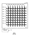
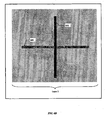
- FIG. 1 depicts a prior art switch matrix 100.
- the switch matrix 100 includes a plurality of overlapping unassociated microstrips 102a-102p arranged to form a grid.
- the microstrips are conductive lines fabricated on a semiconductor substrate 104, which is typically GaAs to minimize signal losses.
- the microstrips are electrically isolated from one another.
- a switch represented by the diode symbol in FIG. 1 ), e.g., switch 106, is present at each cross point to couple the microstrips that intersect at that cross point.
- Each switch can either be open (i.e., prevent an electrical connection from being made through the switch) or closed (i.e., permit an electrical connection to be made through the switch).
- the switch matrix 100 can be used to route electrical signals. For example, if an input electrical signal is present on horizontal microstrip 102a and only the switch 106 in the upper left hand corner of the switch matrix 100 is closed, the input electrical signal is passed to vertical microstrip 102i. If only the switch 108 in the upper right hand corner of the switch matrix 100 is closed, the input electrical signal is passed to vertical microstrip 102p. Closing of multiple switches will allow the input electrical signal to be passed to multiple microstrips.
- a known switch commonly used in prior art switch matrices is a PNPN latching device.
- the PNPN latching device is coupled between a horizontal microstrip and a vertical microstrip and includes a biasing port for receiving a typical biasing current.
- the PNPN latching device is closed by applying a large differential voltage across the device. For example, if switch 106 is a PNPN latching device, switch 106 may be closed by supplying a positive voltage, e.g., greater than 10 V, to horizontal microstrip 102a and a negative voltage, e.g., less than -10 V, to vertical microstrip 102i.
- the PNPN latching device Once the PNPN latching device is closed, the PNPN latching device will remain closed as long as a relatively small biasing current is passing through the PNPN latching device.
- the PNPN latching device may be opened by removing this biasing current, thereby uncoupling microstrips 102a and 102i. This switching action is due to the inherent hysteresis of the PNPN device, which is well known to those skilled in the art.
- Switch matrices of this type have four significant limitations.
- isolation can be less than -20dB at 25 Gigahertz.
- the GaAs substrates that are typically used in switch matrices to minimize signal losses are relatively expensive as compared to silicon substrates.
- Third, the PNPN latching devices that are commonly used are difficult to design and produce, leading to relatively high fabrication costs. Finally, due to size and yield restrictions, it is difficult to incorporate amplifiers into the switch matrix to amplify the RF signal.
- US patent 5073755 discloses a crosspoint matrix having matrix input lines which lead via pairs of switching elements to matrix output lines having, respectively, two signal conductors which are respectively connectible to a reference potential source via a precharging transistor controlled by a precharging clock and which have signal inputs of differential amplifier with a trigger behavior connectible thereto.
- EP patent application 0755093A1 discloses a wireless communication system which employs Butler matrix combiners and circuit switching at transmitter and receiver antenna arrays to provide directive beamwidth capabilities
- the present invention is a switch matrix of claim 1; a corresponding switch matrix assembly of claim 18; a corresponding method of claim 31.
- the signals on a pair of microstrips are preferably balanced such that the electromagnetic fields produced by each of the microstrips at a midpoint between the microstrips are canceled by the electromagnetic fields produced by the other to create a virtual ground at the midpoint.
- the electromagnetic fields produced by a balanced microstrip pair are concentrated primarily in the vicinity of a circular region centered around the midpoint between the two microstrips of the microstrip pair and perpendicular to the longitudinal axes of the microstrips, rather than being concentrated into the semiconductor substrate as in conventional unbalanced microstrips.
- increased isolation is achieved between the microstrip pair and the semiconductor substrate, which minimizes losses due to the semiconductor substrate.
- microstrip pairs are preferably oriented with respect to one another such that the electromagnetic fields produces by each microstrip pair cancels the electromagnetic fields produced by the microstrip pairs they cross, e.g., are oriented perpendicular to one another, to reduce coupling between these microstrip pairs. Accordingly, increased isolation is achieved between microstrip pairs that cross.
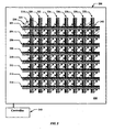
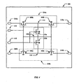
- FIG. 2 depicts an embodiment of a switch matrix 200 for routing electrical signals in accordance with the present invention.
- the switch matrix 200 includes microstrip pairs 202-232 and switch assemblies (represented by diode pairs in FIG. 2 ), e.g., switch assembly 234. Switch assemblies are associated with each point where one microstrip pair crosses another, e.g., cross point 236, for electrically coupling the microstrip pairs that cross at that cross point, e.g., microstrip pairs 202, 218.
- the microstrip pairs 202-232 comprise a pair of associated or correlated microstrips and are fabricated on a semiconductor substrate 238 in a grid pattern, e.g., an 8 X 8 grid.
- Each microstrip pair 202-232 includes a pair of microstrips substantially parallel to one another.
- the first set of microstrip pairs is substantially perpendicular to the second set of microstrip pairs such that the microstrip pairs are perpendicular to one another at each cross point.
- the electromagnetic fields produces by each microstrip pair cancels the electromagnetic fields produced by the microstrip pairs they cross, thereby reducing coupling between the microstrip pairs at the cross points. Accordingly, increased isolation is achieved between the microstrip pairs at the cross points.
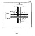
- FIG. 2A is a detailed view of exemplary cross point 236 of FIG. 2 .
- first microstrip pair 202 having a horizontal orientation crosses second microstrip pair 218 having a vertical orientation.
- the first microstrip pair 202 includes a first microstrip 202a and a second microstrip 202b substantially parallel to one another.
- the second microstrip pair 218 includes a first microstrip 218a (a third microstrip 218a) and a second microstrip 218b (a fourth microstrip 218b) substantially parallel to one another.
- the microstrip pairs 202, 218 are separated by a dielectric layer (not shown), e.g., an air or oxide layer.
- a switch assembly 234 is coupled between the microstrip pairs 202, 218.
- the switch assembly 234 includes a first switch 234a coupled between microstrip 202a and microstrip 218a and a second switch 234b coupled between microstrip 202b and microstrip 218b.
- both switches 234a and 234b are open (i.e., neither switch conducting), thereby preventing coupling between the microstrip pair 202 and microstrip pair 218.
- both switches are closed (i.e., both switches conducting), thereby coupling microstrip pair 202 to microstrip pair 218, i.e., coupling microstrip 202a to microstrip 218a and coupling microstrip 202b to microstrip 218b.
- the electrical signal When routing electrical signals, preferably, the electrical signal are introduced to the microstrip pairs such that the microstrip pairs through which the electrical signals pass are balanced.
- the electrical signals passing through the microstrips produce electromagnetic fields that couple to the semiconductor substrate.
- the electromagnetic fields are concentrated primarily in the vicinity of a circular region centered around a midpoint between the two microstrips of the microstrip pair and perpendicular to the longitudinal axes of the microstrips, rather than being concentrated into the semiconductor substrate as in conventional unbalanced microstrips. This reduces coupling to the semiconductor substrate, thereby reducing signal losses attributable to the semiconductor substrate.
- acceptable levels of signal losses may be achieved using an inexpensive semiconductor substrate such as silicon.
- relatively expensive semiconductor substrates such as GaAs were required to reduce coupling between a microstrip and the substrate.
- microstrip pair 202 To balance a microstrip pair, such as microstrip pair 202, electrical signals are introduced to the pair in a manner that produces a first current in a first microstrip 202a that flows in a first direction and a second current in a second microstrip 202b that flows in an opposite direction.
- the first and second currents are equal in magnitude, but are 180 degrees out of phase. Since the currents are equal in magnitude and 180 degrees out of phase, the center between the two microstrips is a virtual ground. Thus, the electromagnetic fields produced by the microstrip pair 202 is minimized.
- the electrical signal is a digital data signal made up of a series of high and low values. At any given instant, one microstrip of a microstrip pair has a high value and the other microstrip of the microstrip pair has a low value.
- a differential amplifier such as described below in reference to FIG. 3 may be used to introduce signals to a microstrip pair so that the microstrip pair is balanced.
- a controller 240 is coupled to the switch matrix 200.
- the controller 240 is a conventional controller such as a digital signal processor (DSP), state machine, microprocessor, micro-controller, logic circuit, or essentially any device capable of processing electrical signals.
- DSP digital signal processor
- the controller 240 is coupled to the switch matrix via a differential amplifier such as the differential amplifier described below in reference to FIG. 3 .
- the controller 240 operates in a switching mode and in a signaling mode.
- the controller 240 configures the switch matrix 200 by opening/closing individual switch assemblies to electrically couple select ones of the microstrip pairs, which is described in greater detail below.
- the controller 240 supplies electrical signals to the microstrip pairs for routing by the switch matrix 200 as configured during the switching mode. For example, if, during the switching mode, the switch assembly 234 in the upper left hand corner of the switch matrix 200 is closed and a signal is applied to the first horizontal microstrip pair 202 during the signaling mode, the signal will be routed onto the first vertical microstrip pair 218.
- the signal will be routed onto the last vertical microstrip pair 232.
- data supplied by the controller 240 e.g., through a differential amplifier, is introduced to the microstrip pairs such that those microstrip pairs are balanced.
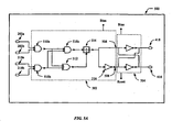
- FIG. 3 depicts an amplifier 300 for use with the switch matrix 200 of FIG. 2 .
- Separate amplifiers 300 are preferably coupled between the controller 240 ( FIG. 2 ) and each microstrip pair 202-232. In certain embodiments, amplifiers 300 are also coupled between each microstrip pair 202-232 and an output device(s) (not shown). Each amplifier 300 may be used to introduce gain to the data signals being routed by the switch matrix 200 and to provide impedance matching between the switch matrix 200 ( FIG. 2 ) and the controller 240/output device(s) to which it is coupled.
- the illustrated amplifier 300 includes a pair of input ports 302a and 302b, a pair of output ports 304a and 304b, and a control port 306.
- the amplifier 300 is configured via the control port 306 (e.g., by the controller 240) to operate in either a data signaling mode or a switching mode.
- applying a first value, e.g., a low voltage value of less than about 0.2 V, to the control port 306 configures the amplifier 300 in a switching mode and applying a second value, e.g., a high voltage value greater than about 1.0 V, to the control port 306 configures the amplifier 300 in a signaling mode.
- a differential signal applied between the pair of input ports 302a and 302b (a differential input) will be amplified and presented as an amplified differential signal between the pair of output ports 304a and 304b for introduction between the microstrips of a microstrip pair, e.g., microstrips 202a and 202b of microstrip pair 202.
- the differential signal introduced between the microstrips results in a balanced microstrip pair as described in detail above.
- both output ports 304a and 304b will present a switch set value, e.g., a high value greater than about 3.0 V, to be placed on both of the microstrips of the microstrip pair, which, as will be described in detail below, is a necessary step for closing the switch assembly 234 ( FIG. 2 ) using the control depicted in FIG. 5A .
- the amplifier 300 includes a control transistor 308 for receiving the control signal for configuring the amplifier 300 in either the data signaling mode or the switching mode and a pair of transistor 31 0a and 310b having control ports for receiving the differential signal applied between the input ports 302a and 302b.
- the current flow terminals of each transistor of the transistor pair are coupled between a voltage source 312, e.g., a 3.0 V DC voltage source, and the current flow terminals of the control transistor 308.
- the amplifier 300 is configured in the signal mode by applying a high signal to the control transistor 308 via the control port, which turns on the control transistor to allow current flow through the pair of transistors 310a and 310b. In this mode, the amplifier 300 of FIG.
- the amplifier 300 behaves as a conventional differential amplifier and a differential signal between the input ports 302a and 302b will be amplified and presented between the output ports 304a and 304b.
- the amplifier 300 is configured in the switching mode by applying a low signal to the control transistor 308 via the control port, which turns off the control transistor 308. In this mode, current is prevented from flowing through the pair of transistors 310a and 310b, which effectively turns off these transistors and results in a high value, e.g., the 3.0 V, from the voltage source 312, being presented at the pair of output ports 304a and 304b.
- FIG. 4 depicts a preferred cross point switch 400 for use in the switch assembly 234 of FIG. 2 to couple microstrip pairs at a cross point.
- the illustrated cross point switch 400 includes a first switch 234a for coupling a first microstrip 202a of a first microstrip pair 202 to a first microstrip 218a (a third microstrip 218a) of a second microstrip pair 218, a second switch 234b for coupling a second microstrip 202b of the first microstrip pair 202 to a second microstrip 218b (a fourth microstrip 218b) of the second microstrip pair 218, and a third switch 402 (an "isolation switch”) for coupling the first and second switches 234a and 234b together when the first and second switches are open to improve isolation at the cross point.
- a third switch 402 an "isolation switch"
- the first switch 234a includes a first transistor 406a and a second transistor 406b coupled in series between microstrip 202a and microstrip 218a such that when both transistors are on these microstrips are coupled together through the transistors current flow terminals, e.g., the collector/emitter of a BJT or the drain/source of a FET.
- the second switch 234b includes a first transistor 408a and a second transistor 408b coupled in series between microstrip 202b and microstrip 218b such that when both transistors are on these microstrips are coupled together.
- the third switch 402 includes a first transistor 410a and a second transistor 410b coupled in series between the first and second switches 234a and 234b such that when both transistors are on a connection point 412 between the transistors of the first switch 234a is coupled to a connection point 414 between the transistors of the second switch 234b. All transistors can be turned on by supplying a switch value, e.g., a high voltage (and turned off by supplying a low voltage), to the control terminals of the transistors, i.e., the base of a BJT or the gate of a FET.
- a switch value e.g., a high voltage (and turned off by supplying a low voltage
- the control terminals of the transistors within the first and second switches 234a and 234b are coupled to a first switch port 416 and the control terminals of the transistors within the third switch 402 are coupled to a second switch port 418.
- the switch assembly 234 ( FIG. 1 ) is closed when a high value is applied to the first switch port 416 (which turns on the transistors of the first and second switches 234a and 234b) and a low value is applied to the second switch port 418 (which turns off the transistors of the third switch 402).
- the switch assembly 234 is open when a low value is applied to the first switch port 416 (transistors of switches 234a and 234b off) and a high value is applied to the second switch port 418 (transistors of switch 402 on). It will be readily apparent to those skilled in the art that the transistors of the third switch 402, which are on when the switch assembly 234 is open, will improve isolation between microstrip pairs (e.g., between microstrips 202 and 218) at the cross point when the switch assembly 234 is open.
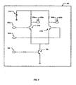
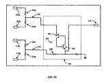
- FIG. 5A depicts one embodiment of a control circuit 500 for use in the switch assembly 234 of FIG. 2 to control the cross point switch 400 of FIG. 4 .
- the illustrated control circuit 500 controls the values presented to the first and second switch ports 416, 418 of the cross point switch 400 in response to signal levels on the microstrips.
- the control circuit 500 includes a logic circuit 502 and a latch 504.
- the switch assembly 234 is closed when the latch 504 is set.
- the logic circuit 502 sets the latch 504, thereby closing the switch assembly 234 in response to specific signal levels on the microstrips, e.g., a high value on each of the microstrips associated with the switch assembly 234.
- the latch 504 may then be reset, thereby opening the switch assembly 234.
- the logic circuit 502 is a conventional logic circuit for controlling the latch 504 in response to values present on the microstrips.
- the logic circuit 502 initially presents a low value at a first output point 506 and a high value at a second output point 508.
- the logic circuit 502 will then present a high value at the first output point 506 and a low value at the second output point 508 in response to high values present on each of the microstrips.
- the logic circuit 502 will present a low value at the first output point 506 and a high value at the second output point 508.
- a high value on each of the microstrips which are coupled to the inputs of a first AND gate 510a and a second AND gate 510b, will produce a high value at the outputs of the first and second AND gates 510a and 510b.
- the outputs of the first and second AND gates 510a and 510b are coupled to the inputs of an OR gate 512 and the inputs of a third AND gate 510c, thereby causing high values at the outputs of the OR gate 512 and the third AND gate 510c.
- the high output from the OR gate 512 closes a conventional switch 514 (e.g., a transistor), which allows the high output from the third AND gate 510c to pass through the switch 514 to the first output point 506.
- the high output passes through an inverter 516 to produce a low value at the second output point 508. If any one of the microstrips presents a low value, a low value passes to the first output point 506 and a high value passes to the second output point 508.
- the latch 504 presents a low value at the first switch port 416 and a high value at the second switch port 418 (i.e., the switch assembly 234 will be open).
- the latch 504 presents a high value at the first switch port 416 and a low value at the second switch port 418 (i.e., the switch assembly 234 will be closed).
- the latch is set in response to a high value at the first output point 506 of the logic circuit 502 and a low value at the second output point 508 of the logic circuit 502.
- the latch 504 When reset, the latch 504 presents a low value at the first switch port 416 and a high value at the second switch port 418 (i.e., the switch assembly 234 will be open).
- the latch 504 is a conventional latch that is reset in a known manner by supplying a reset signal to a reset port (RESET) common to such latches.
- the latch 504 is a conventional latch that is reset in a known manner by reducing a bias voltage applied to a bias port (BIAS) also common to such latches.
- RESET reset signal to a reset port
- BIOS bias voltage applied to a bias port
- the reset signal could be generated by a reset logic circuit (not shown) coupled to the microstrips, e.g., microstrips 202a, 202b, 218a, and 218b.
- the reset logic circuit could be configured to reset the latch 504 in response to a low value on all microstrips coupled to the logic circuit.
- the latch 504 is a conventional JK flip-flop that may be reset using the same values used to set the latch 504, i.e., a high value at the first output point 506 and a low value at the second output point 508. For example, a high value at a first output point 506 and a low value at a second output point 508 will set the latch 504 after the latch has been reset. Likewise, applying the same values to the latch after the latch has been set will reset the latch.
- signals are applied to each of the microstrip pairs by a controller 240 ( FIG. 2 ) via an amplifier 300 ( FIG. 3 ).
- the amplifier 300 is configured in a data signaling mode, e.g., by applying a high value to the control port 306 of the control transistor 308 of the amplifier 300, a differential signal across the input ports 302a, b of the amplifier 300 is amplified and presented at the output ports 304a, b of the amplifier 300 for passage onto the microstrips coupled to the output ports 304a, b.
- the amplifier 300 is configured in a switching mode, e.g., by applying a low value to the control port 306 of the control transistor 308 of the amplifier 300, high values are presented at the output ports 304a and 304b of the amplifier 300 for passage onto the microstrips.
- the controller 240 configures the switch matrix 200 for routing data signals by selectively controlling which of the switch assemblies are closed.
- a switch assembly is closed if the switches between the microstrip pairs coupled to the switch assembly are closed.
- switch assembly 234 is closed if switches 234a and 234b are closed. If the switches 234a and 234b are open, these switches may be closed by applying high values to each microstrip for the microstrip pairs coupled to the switch assembly 234, e.g., microstrips 202a, 202b, 218a, and 218b. High values are applied to these microstrips by applying a low value to the control port 306 of each of the control transistors 308 of amplifiers 300 associated with the microstrip pairs 202 and 218.
- Applying high values to each of the microstrips prompts the logic circuit 502 ( FIG. 5A ) to be configured such that a high value is presented on the first switch port 416 and a low value is presented on the second switch port 418.
- the high value on the first switch port 416 and the low value on the second switch port 418 cause the switches 234a and 234b within the switch assembly 234 that are coupled between the microstrip pairs 202 and 218 to close, thereby coupling the first microstrip 202a of the first microstrip pair 202 to the first microstrip 218a of the second microstrip pair 218 and coupling the second microstrip 202b of the first microstrip pair 202 to the second microstrip 218b of the second microstrip pair 218.
- Switch assemblies that are closed may be opened using techniques such as those described above with reference to the logic circuit 502 of FIG. 5A .
- the data signals are then routed by the switch matrix 200 as configured by the controller 240.
- the switch matrix 200 is configured such that switch assembly 234 is closed and a data signal is applied as a differential signal across microstrips 202a, b, that data signal will be routed to produce a differential signal across microstrips 218a, b.
- FIGS. 5B , 5C , and 5D depict alternative control circuits for controlling the cross point switch 400 of FIG. 4 .
- These alternative control circuits may be used to develop an output signal to set the voltage level at the first switch port 416 of the cross point switch 400.
- the development of a complementary output signal to set the voltage level at the second switch port 418 will be readily apparent to one of skill in the art.
- Each of the control circuits depicted in FIGS. 5B , 5C , and 5D set the voltage level at the first switch port 416 based on a first tapped signal on a first tap line 520 developed from signals on a corresponding microstrip pair, e.g., microstrip pair 202, and a second tapped signal on a second tap line 522 developed from signals on a corresponding other microstrip pair, e.g., microstrip pair 218.
- each control line 520, 522 is located at the midpoint between its corresponding microstrip pair 202, 218.
- a first resistor 524a is coupled between a first microstrip 202a and the first tap line 520
- a second resistor 524b is coupled between a second microstrip 202b and the first tap line 520
- a third resistor 524c is coupled between a third microstrip 218a and the second tap line 522
- a fourth resistor 524d is coupled between a fourth microstrip 218b and the second tap line 522.
- the resistors 524a-d are high-value resistors having a resistance that is greater than about 10 KOhms.
- microstrip pairs When the microstrip pairs are balanced (e.g., during a data signaling after a switching mode), a virtual ground exists at the midpoint between the microstrips and, thus, no coupling will occur between the microstrip pairs and the corresponding tap line. Since no coupling occurs during data signaling, insertion losses attributed to the control circuit can be minimized. If the microstrips of a microstrip pair become unbalanced, RF coupling occurs between the microstrips of the microstrip pair and the corresponding tap line and, thus, a signal will be developed on the tap line. The development of signals needed on the microstrip pairs to develop the signals on the tap lines ("tapped signals") for controlling the control circuits depicted in FIGS. 5B , 5C , and 5D will be readily apparent to those skilled in the art.
- FIG. 5B depicts an integrator control circuit 530.
- the illustrated integrator control circuit 530 includes a logic circuit 532 and an integrator 534.
- the logic circuit 532 includes an exclusive OR gate 536 and an inverter 538, and the integrator 534 can be implemented using a shunt capacitor.
- the logic circuit 532 develops a scalar product of the tapped signals received on the first and second tap lines 520, 522 and the integrator 534 integrates the scalar product. If the tapped signals on the first and second tap lines are the same, the integrator 534 will produce a maximum output, e.g., 3.0 V, at the first switch port 416. When the maximum value is produced at the first switch port 416, the cross point switch 400 ( FIG.
- the cross point switch 400 is open. It will be readily apparent to those skilled in the art that if two or more cross point switches corresponding to two or more cross points are to be closed at the same time, one tapped signal may be developed by the microstrips corresponding to one of the cross points for closing switches at that cross point and another tapped signal may be developed by the microstrips corresponding to another one of the cross points for closing switches at that cross point.
- the tapped signals on the first and second tap lines 520, 522 need to be applied continuously to keep the cross point switch 400 closed - even when using the switch matrix 200 to pass data signals.
- the signals on the tap lines can be applied during the passage of data signals by adding identical voltage level signals to each microstrip of a microstrip pair. Since data signals are passed along each microstrip pair as a differential signal, as long as the differential voltage between the microstrips remains unchanged, the integrity of the data signal can be preserved.
- the signals on the microstrip pairs used to create the tapped signals on the tap lines can "ride" on the same line as the data signals as long as the voltage levels on both microstrips of a microstrip pair move up and down at the same time. Additionally, different frequencies can be used for the control signals and for the data signals to further increase the separation of these signals.
- FIG. 5C depicts a logic control circuit 550.
- the illustrated logic control circuit 550 includes an AND gate 552 and a conventional toggle flip-flop 554.
- a first input of the AND gate 552 is coupled to a first tap line 520 to receive a first tapped signal and a second input of the AND gate is coupled to a second tap line 522 to receive a second tapped signal.
- An output of the AND gate is coupled to the clock port (CLK) of the flip-flop 554.
- the output (Q) of the flip-flop 554 is coupled to the first switch port 416.
- the values of the first and second tapped signals at the inputs of the AND gate and the output of the flip-flop 554 are initially low, which results in an open corresponding cross point switch 400 ( FIG. 4 ).
- the output of the AND gate 552 transitions from low to high, which, in turn, toggles the output (Q) of the flip-flop 554 from low to high, thereby closing the corresponding cross point switch.
- the tapped signals at the inputs of the AND gate 552 are then set low and the closed cross point switch may be used to pass data signals.
- the output of the AND gate 552 transitions from low to high, which, in turn, toggles the output of the flip-flop 554 from high to low, thereby opening the corresponding cross point switch which ceases the data signal transmission.
- FIG. 5D depicts a thyristor control circuit 560.
- the thyristor control circuit 560 includes a conventional thyristor 562, which includes a first transistor 564 and a second transistor 566.
- the emitter of the first transistor 564 is coupled to the first tap line 520 to receive a first tapped signal and the emitter of the second transistor 566 is coupled to the second tap line 522 through a resistor 568 to receive a second tapped signal.
- the emitter of the second transistor 566 is also coupled to the first switch port 416 for controlling a corresponding cross point switch 400 ( FIG. 4 ).
- a voltage across the thyristor 562 e.g., between the emitter of the first transistor 564 and the emitter of the second transistor 566, that exceeds the breakdown voltage of the thyristor 562, turns on the thyristor 562, which, in turn, produces a high value at the first switch port 416 to close the corresponding cross point switch.
- the thyristor will remain on as long as a "hold-on" current flows through the thyristor 560 between the emitter of the first transistor 564 and the collector of the second transistor 566.
- the hold-on current may be supplied to the thyristor 560 in a manner similar to the switching signals applied to the integrator control circuit 530 of FIG. 5B . Reducing the current flowing through the thyristor 560 below the hold-on current, turns off the thyristor, which, in turn, produces a low value at the first switch port 416 to open the corresponding cross point switch.
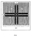
- FIGS. 6A and 6B depict a preferred method for routing of biasing lines within the switch matrix 200 of FIG. 2 .
- the biasing lines may be used to bias the components of the switches.
- bias lines may be used to bias the logic circuits 502, 504 and switches 234a, 234b, 402 depicted in FIG. 4 .
- the microstrip pairs, e.g., microstrip pairs 202 and 218, of the switch matrix 200 are located in one layer (e.g., layer 1) and, as depicted in FIG.
- the biasing lines such as biasing lines 600 and 602 are located in another layer (e.g., layer 2) to facilitate fabrication and maintain electrical isolation between the microstrips and the biasing lines.
- the first bias line 600 ( FIG. 6B ) is positioned between a first microstrip 202a and a second microstrip 202b of a first microstrip pair 202 ( FIG. 6A ) and a second bias line 602 ( FIG. 6B ) is positioned between a first microstrip 218a (a third microstrip 218a) and a second microstrip 218b (a fourth microstrip 218b) of a second microstrip pair 218 ( FIG. 6A ).
- FIG. 7A is a graph illustrating the coupling characteristics of a simulated cross point between conventional microstrips in decibels (dB) for frequencies between 0 and 40 Gigahertz.
- the simulation was rendered in Sonnet® (a computer software program well known to those of skill in the art that enables the simulation of electromagnetic fields) using 25 micrometer microstrips, e.g., microstrip 102a and microstrip 102i ( FIG. 1 ), over a 100 micrometer GaAs substrate.
- the coupling is approximately -20dB.
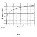
- FIG. 7B is a graph illustrating the coupling characteristics of a simulated cross point between balanced microstrip pairs in accordance with the present invention for frequencies between 0 and 40 Gigahertz.
- the simulation was also rendered in Sonnet@ using 25 micrometer microstrips, e.g., microstrips 202a and 202b and microstrips 218a and 218b ( FIG. 2A ), over a 250 micrometer silicon substrate.
- the bulk resistivity is 20 Ohms-cm.
- the coupling is approximately -70dB. Accordingly, much better isolation is achieved than in the conventional approach.
Landscapes
- Electronic Switches (AREA)
- Waveguide Switches, Polarizers, And Phase Shifters (AREA)
Claims (35)
- Matrice de commutation comportant:une pluralité de paires de guides d'ondes à rubans (202 - 232), où une première desdites paires de guides d'ondes à rubans traverse une deuxième desdites paires de guides d'ondes à rubans à un point de croisement (236); etun ensemble commutateur (234) associé audit point de croisement (236) pour coupler ladite première paire de guides d'ondes à rubans (202) à ladite deuxième paire de guides d'ondes à rubans (218),caractérisé en ce que ledit ensemble commutateur est actionné sur la base de signaux échelonnés développés à partir de signaux sur lesdites première et deuxième paires de guides d'ondes à rubans.
- Matrice de commutation selon la revendication 1, comportant en outre:un substrat semi-conducteur (238) sur lequel ladite pluralité de paires de guides d'ondes à rubans (202 - 232) est fabriquée, ledit substrat semi-conducteur étant du silicium.
- Matrice de commutation selon la revendication 1 ou 2, dans laquelle chacune de ladite pluralité de paires de guides d'ondes à rubans (202 - 232) comporte au moins:un premier guide d'ondes à rubans (202a, 218a); etun deuxième guide d'ondes à rubans (202b, 218b) sensiblement parallèle audit premier guide d'ondes à rubans (202a, 218a);dans lequel, au cours d'un acheminement de signal par ladite matrice de commutation (200), lorsqu'un premier signal est transmis sur ledit premier guide d'ondes à rubans (202a, 218a) de l'une de ladite pluralité de paires de guides d'ondes à rubans, un second signal est transmis sur ledit deuxième guide d'ondes à rubans (202b, 218b) de ladite une paire de ladite pluralité de paires de guides d'ondes à rubans de sorte que ladite une paire de ladite pluralité de paires de guides d'ondes à rubans est équilibrée.
- Matrice de commutation selon la revendication 3, dans laquelle ledit premier guide d'ondes à rubans (202a, 218a) produit une première force électromagnétique lorsque ledit premier signal passe à travers ledit premier guide d'ondes à rubans et ledit deuxième guide d'ondes à rubans (202b, 218b) produit une seconde force électromagnétique lorsque ledit second signal passe à travers ledit deuxième guide d'ondes à rubans, les forces électromagnétiques produites par chacun desdits premiers et deuxièmes guides d'ondes à rubans annulant au moins partiellement les forces électromagnétiques produites par l'autre.
- Matrice de commutation selon la revendication 1, dans laquelle ladite première paire de guides d'ondes à rubans (202) comporte au moins un premier guide d'ondes à rubans (202a) et un deuxième guide d'ondes à rubans (202b) sensiblement parallèle audit premier guide d'ondes à rubans (202a) et où ladite deuxième paire de guides d'ondes à rubans (218) comporte au moins un troisième guide d'ondes à rubans (218a) et un quatrième guide d'ondes à rubans (218b) sensiblement parallèle audit troisième guide d'ondes à rubans (218a).
- Matrice de commutation selon la revendication 5, dans laquelle ledit ensemble commutateur comporte au moins:un premier commutateur (234a) couplé entre ledit premier guide d'ondes à rubans (202a) et ledit troisième guide d'ondes à rubans (218a); etun deuxième commutateur (234b) couplé entre ledit deuxième guide d'ondes à rubans (202b) et ledit quatrième guide d'ondes à rubans (218b).
- Matrice de commutation selon la revendication 6, comportant en outre au moins:un contrôleur (240) couplé auxdits premier, deuxième, troisième et quatrième guides d'ondes à rubans pour fermer lesdits premier et deuxième commutateurs (234a, 234b).
- Matrice de commutation selon la revendication 6, dans laquelle ledit ensemble commutateur comporte en outre un circuit logique (502, 532, 550, 560) pour actionner lesdits premier et deuxième commutateurs (234a, 234b), ledit circuit logique (502, 532, 550, 560) présentant des entrées couplées auxdits premier, deuxième, troisième et quatrième guides d'ondes à rubans (202a, 202b, 218a, 218b) et des sorties couplés auxdits premier et deuxième commutateurs (234a, 234b), ledit circuit logique (502, 532, 550, 560) fermant lesdits premier et deuxième commutateurs (234a, 234b) lorsqu'une valeur de commutateur est reçue sur lesdits premier, deuxième, troisième et quatrième guides d'ondes à rubans.
- Matrice de commutation selon la revendication 8, comportant en outre un contrôleur (240) couplé auxdits premier et deuxième guides d'ondes à rubans pour fournir ladite valeur de commutateur auxdits premier et deuxième guides d'ondes à rubans.
- Matrice de commutation selon la revendication 9, comportant en outre un amplificateur (300) couplé entre ledit contrôleur (240) et lesdits premier et deuxième guides d'ondes à rubans (202a, 202b), ledit amplificateur (300) comportant une entrée différentielle configurée pour recevoir un signal différentiel provenant dudit contrôleur (240), une entrée de commutation configurée pour recevoir une valeur définie de commutateur provenant du contrôleur (240), une première sortie d'amplificateur (304a) couplée audit premier guide d'ondes à rubans (202a), et une seconde sortie d'amplificateur (304b) couplée audit deuxième guide d'ondes à rubans (202b), dans laquelle, lorsque ladite valeur définie de commutateur est à un premier niveau, ledit amplificateur (300) présente une version amplifiée dudit signal différentiel entre lesdites première et seconde sorties d'amplificateur et, lorsque ladite valeur définie de commutateur est à un second niveau, une valeur de commutateur est présentée au niveau desdites première et seconde sorties d'amplificateur (304a, 304b).
- Matrice de commutation selon la revendication 6 ou 7, dans laquelle ledit ensemble commutateur (234) comporte au moins un circuit logique (532, 550, 560) pour actionner lesdits premier et deuxième commutateurs (234a, 234b), ledit circuit logique présentant une première entrée couplée à une première ligne de prélèvement (520) positionnée entre lesdits premier et deuxième guides d'ondes à rubans (202a, 202b) et une seconde entrée couplée à une seconde ligne de prélèvement (522) positionnée entre lesdits troisième et quatrième guides d'ondes à rubans (218a, 218b), ledit circuit logique (532, 550, 560) fermant lesdits premier et deuxième commutateurs (234a, 234b) lorsqu'un premier signal échelonné est développé sur ladite première ligne de prélèvement (520) par des signaux sur lesdits premier et deuxième guides d'ondes à rubans et un second signal échelonné est développé sur ladite seconde ligne de prélèvement (522) par des signaux sur lesdits troisième et quatrième guides d'ondes à rubans.
- Matrice de commutation selon la revendication 11, dans laquelle ladite première ligne de prélèvement (520) est positionnée à un premier point médian entre lesdits premier et deuxième guides d'ondes à rubans (202a, 202b) et ladite seconde ligne de prélèvement (522) est positionnée à un deuxième point médian entre lesdits troisième et quatrième guides d'ondes à rubans (218a, 218b), où lesdits premier et deuxième signaux échelonnés sont des signaux de radiofréquence (RF) développés sur lesdites première et seconde lignes de prélèvement (520, 522) au cours d'une commutation, et où, postérieurement à la commutation, ledit premier point médian est une masse virtuelle entre lesdits premier et deuxième guides d'ondes à rubans (202a, 202b) et ledit deuxième point médian est une masse virtuelle entre lesdits troisième et quatrième guides d'ondes à rubans (218a, 218b).
- Matrice de commutation selon la revendication 6 ou 7, dans laquelle ledit ensemble commutateur comporte en outre au moins un circuit logique (532) et un intégrateur (534) pour actionner lesdits premier et deuxième commutateurs (234a, 234b), ledit circuit logique (532) présentant une première entrée couplée à une première ligne de prélèvement (520) positionnée entre lesdits premier et deuxième guides d'ondes à rubans (202a, 202b) et une seconde entrée couplée à une seconde ligne de prélèvement (522) positionnée entre lesdits troisième et quatrième guides d'ondes à rubans (218a, 218b), ledit circuit logique (532) produisant un produit scalaire d'un premier signal échelonné développé sur ladite première ligne de prélèvement (520) par des signaux sur lesdits premier et deuxième guides d'ondes à rubans et un second signal échelonné développé sur ladite seconde ligne de prélèvement (522) par des signaux sur lesdits troisième et quatrième guides d'ondes à rubans, lesdits premier et deuxième commutateurs (234a, 234b) étant fermés sur la base d'une intégration dudit produit scalaire.
- Matrice de commutation selon la revendication 13, dans laquelle ladite première ligne de prélèvement (520) est positionnée à un premier point médian entre lesdits premier et deuxième guides d'ondes à rubans (202a, 202b) et ladite seconde ligne de prélèvement (522) est positionnée à un deuxième point médian entre lesdits troisième et quatrième guides d'ondes à rubans (218a, 218b), où lesdits premier et deuxième signaux échelonnés sont des signaux de radiofréquence (RF) développés sur lesdites première et seconde lignes de prélèvement (520, 522) au cours d'une commutation, et où, postérieurement à la commutation, ledit premier point médian est une masse virtuel entre lesdits premier et deuxième guides d'ondes à rubans (202a, 202b) et ledit deuxième point médian est une masse virtuelle entre lesdits troisième et quatrième guides d'ondes à rubans (218a, 218b).
- Matrice de commutation selon la revendication 6 ou 7, dans laquelle ledit ensemble commutateur (234) comporte au moins un thyristor (560) présentant une tension de claquage pour actionner lesdits premier et deuxième commutateurs, ledit thyristor (560) présentant une première entrée couplée à une première ligne de prélèvement (520) positionnée entre lesdits premier et deuxième guides d'ondes à rubans (202a, 202b) et une seconde entrée couplée à une seconde ligne de prélèvement (522) positionnée entre lesdits troisième et quatrième guides d'ondes à rubans (218a, 218b), ledit thyristor (560) fermant lesdits premier et deuxième commutateurs (234a, 234b) lorsqu'une différence de tension entre lesdites premier et seconde entrées dépasse ladite tension de claquage.
- Matrice de commutation selon l'une quelconque des revendications 1 à 5, dans laquelle ledit ensemble commutateur (234) comporte au moins:un premier commutateur (234a) comportant une paire de transistors (406a, 406b) présentant des bornes de circulation de courant couplées en série entre lesdits premier et troisième guides d'ondes à rubans (202a, 218a) et une borne de commande pour recevoir un premier signal de commande;un deuxième commutateur (234b) comportant une paire de transistors (408a, 408b) présentant des bornes de circulation de courant couplées en série entre lesdits deuxième et quatrième guides d'ondes à rubans (202b, 218b) et une borne de commande pour recevoir ledit premier signal de commande; etune troisième commutateur (402) comportant une paire de transistors (410a, 410b) présentant des bornes de circulation de courant couplées en série entre lesdits premier et deuxième commutateurs (234a, 234b) et une borne de commande pour recevoir un second signal de commande.
- Matrice de commutation selon la revendication 16, dans laquelle ledit ensemble commutateur (234) comporte en outre au moins:un circuit logique (502, 532, 550, 560) pour produire lesdits premier et deuxième signaux de commande, ledit circuit logique (502, 532, 550, 560) présentant des ports d'entrée couplés auxdits premier, deuxième, troisième et quatrième guides d'ondes à rubans (202a, 202b, 218a, 218b), ledit circuit logique produisant lesdits premier et deuxième signaux de commande sur la base de niveaux de signal sur lesdits premier, deuxième, troisième et quatrième guides d'ondes à rubans.
- Dispositif de matrice de commutation comportant:une matrice de commutation selon la revendication 1, présentant une ou plusieurs paires de guides d'ondes à rubans (202 - 216) d'une première orientation; une ou plusieurs paires de guides d'ondes à rubans (218 - 232) d'une deuxième orientation dont chacune traverse ladite une ou lesdites plusieurs paires de guides d'ondes à rubans (202 - 216) de ladite première orientation aux points de croisement (236), chacun desdits points de croisement (236) correspondant au croisement de l'une desdites paires de guides d'ondes à rubans (202 - 216) de ladite première orientation avec une desdites paires de guides d'ondes à rubans (218 - 232) de ladite deuxième orientation, et un ou plusieurs ensembles commutateur (234), chaque ensemble commutateur étant associé à l'un desdits points de croisement (236); etun contrôleur (240) couplé audit un ou plusieurs ensembles commutateur (234) pour fermer des ensembles individuels desdits ensembles commutateur (234) pour coupler des paires sélectionnées de ladite une ou desdites plusieurs paires de guides d'ondes à rubans (202 - 216) de ladite première orientation à ladite une ou auxdites plusieurs paires de guides d'ondes à rubans (218 - 232) de ladite deuxième orientation, ledit contrôleur activant ledit un ou lesdits plusieurs ensembles commutateur sur la base de signaux échelonnés développés à partir de signaux sur ladite une ou lesdites plusieurs paires de guides d'ondes à rubans.
- Dispositif selon la revendication 18, comportant en outre:un substrat semi-conducteur (238) sur lequel lesdites paires de guides d'ondes à rubans (202 - 232) desdites premier et deuxième orientations sont fabriquées, ledit substrat semi-conducteur étant du silicium.
- Dispositif selon la revendication 18 ou 19, dans lequel chacune de ladite une ou desdites plusieurs paires de guides d'ondes à rubans (202 - 216) de ladite première orientation comporte au moins un premier guide d'ondes à rubans (202a) et un deuxième guide d'ondes à rubans (202b) sensiblement parallèle audit premier guide d'ondes à rubans (202a) et dans lequel chacune desdites paires de guides d'ondes à rubans (218 - 232) de ladite deuxième orientation comporte au moins un troisième guide d'ondes à rubans (218a) et un quatrième guide d'ondes à rubans (218b) sensiblement parallèle audit troisième guide d'ondes à rubans (218a).
- Dispositif selon la revendication 20, dans lequel chacun parmi ledit un ou lesdits plusieurs ensembles commutateur (234) associés à l'un desdits points de croisement (236) comporte au moins:un premier commutateur (234a) couplé entre ledit premier guide d'ondes à rubans (202a) et ledit troisième guide d'ondes à rubans (218a); etun deuxième commutateur (234b) couplé entre ledit deuxième guide d'ondes à rubans (202b) et ledit quatrième guide d'ondes à rubans (218b).
- Dispositif selon la revendication 21, dans lequel chacun parmi ledit un ou lesdits plusieurs ensembles commutateur (234) comporte au moins un circuit logique (502, 532, 550, 560) pour actionner lesdits premier et deuxième commutateurs (234a, 234b), ledit circuit logique présentant des entrées couplées auxdits premier, deuxième, troisième et quatrième guides d'ondes à rubans (202a, 202b, 218a, 218b) et des sorties couplées auxdits premier et deuxième commutateurs (234a, 234b), ledit circuit logique (502, 532, 550, 560) fermant lesdits premier et deuxième commutateurs (234a, 234b) lorsqu'un signal de commutateur est reçu sur lesdits premier, deuxième, troisième et quatrième guides d'ondes à rubans.
- Dispositif selon la revendication 21, dans lequel chacun parmi ledit un ou lesdits plusieurs ensembles commutateur (234) comporte au moins un circuit logique (532, 550, 560) pour actionner lesdits premier et deuxième commutateurs (234a, 234b), ledit circuit logique (532, 550, 560) présentant une première entrée couplée à une première ligne de prélèvement (520) positionnée entre lesdits premier et deuxième guides d'ondes à rubans (202a, 202b) et une seconde entrée couplée à une seconde ligne de prélèvement (552) positionnée entre lesdits troisième et quatrième guides d'ondes à rubans (218a, 218b), ledit circuit logique (532, 550, 560) fermant lesdits premier et deuxième commutateurs (234a, 234b) lorsqu'un premier signal échelonné est développé sur ladite première ligne de prélèvement (520) par des signaux sur lesdits premier et deuxième guides d'ondes à rubans et un second signal échelonné est développé sur ladite seconde ligne de prélèvement (522) par des signaux sur lesdits troisième et quatrième guides d'ondes à rubans.
- Dispositif selon la revendication 23, dans lequel ladite première ligne de prélèvement (520) est positionnée au niveau d'une premier point médian entre lesdits premier et deuxième guides d'ondes à rubans (202a, 202b) et ladite seconde ligne de prélèvement (522) est positionnée au niveau d'un deuxième point médian entre lesdits troisième et quatrième guides d'ondes à rubans (218a, 218b), où lesdits premier et deuxième signaux échelonnés sont des signaux de radiofréquence (RF) développés sur lesdites première et seconde lignes de prélèvement (520, 522) au cours d'une commutation, et où, postérieurement à la commutation, ledit premier point médian est une masse virtuelle entre lesdits premier et deuxième guides d'ondes à rubans (202a, 202b) et ledit deuxième point médian est une masse virtuelle entre lesdits troisième et quatrième guides d'ondes à rubans (218a, 218b).
- Dispositif selon la revendication 21, dans lequel chacun parmi ledit un ou lesdits plusieurs ensembles commutateur (234) comporte au moins un circuit logique (532) et un intégrateur (534) pour actionner lesdits premier et deuxième commutateurs (234a, 234b), ledit circuit logique (532) présentant une première entrée couplée à une première ligne de prélèvement (520) positionnée entre lesdits premier et deuxième guides d'ondes à rubans (202a, 202b) et une seconde entrée couplée à une seconde ligne de prélèvement (522) positionnée entre lesdits troisième et quatrième guides d'ondes à rubans (218a, 218b), ledit circuit logique (532) produisant un produit scalaire d'un premier signal échelonné développé sur ladite première ligne de prélèvement (520) par des signaux sur lesdits premier et deuxième guides d'ondes à rubans (202a, 202b) et un second signal échelonné développé sur ladite seconde ligne de prélèvement (522) par des signaux sur lesdits troisième et quatrième guides d'ondes à rubans (218a, 218b), lesdits premier et deuxième commutateurs (234a, 234b) étant fermés sur la base d'une intégration dudit produit scalaire.
- Dispositif selon la revendication 25, dans lequel ladite première ligne de prélèvement (520) est positionnée au niveau d'un première point médian entre lesdits premier et deuxième guides d'ondes à rubans (202a, 202b) et ladite seconde ligne de prélèvement (522) est positionnée au niveau d'un deuxième point médian entre lesdits troisième et quatrième guides d'ondes à rubans (218a, 218b), dans lequel lesdits premier et deuxième signaux échelonnés sont des signaux de radiofréquence (RF) développés sur lesdites premier et seconde lignes de prélèvement (520, 522) au cours d'une commutation, et où, postérieurement à la commutation, ledit premier point médian est une masse virtuelle entre lesdits premier et deuxième guides d'ondes à rubans (202a, 202b) et ledit deuxième point médian est une masse virtuelle entre lesdits troisième et quatrième guides d'ondes à rubans (218a, 218b).
- Dispositif selon la revendication 21, dans lequel chacun parmi ledit un ou lesdits plusieurs ensembles commutateur (234) comporte au moins un thyristor (562) présentant une tension de claquage pour actionner lesdits premier et deuxième commutateurs (234a, 234b), ledit thyristor (562) présentant une première entrée couplée à une première ligne de prélèvement (520) positionnée entre lesdits premier et deuxième guides d'ondes à rubans (202a, 202b) et une seconde entrée couplée à une seconde ligne de prélèvement (522) positionnée entre lesdits troisième et quatrième guides d'ondes à rubans (218a, 218b), ledit thyristor (562) fermant lesdits premier et deuxième commutateurs (234a, 234b) lorsqu'une différence de tension entre lesdites première et seconde entrées dépasse ladite tension de claquage.
- Dispositif selon l'une quelconque des revendications 20 à 27, comportant en outre:un amplificateur (300) présentant un port de commutateur couplé audit contrôleur et des ports de sortie (304a, 304b) couplés auxdits premier et deuxième guides d'ondes à rubans (202a, 202b), ledit amplificateur produisant une valeur définie de commutateur sur chacun desdits premier et deuxième guides d'ondes à rubans lorsqu'une valeur de commutateur est présente sur ledit port de commutateur.
- Dispositif selon la revendication 18 ou 19, dans lequel chacune de ladite une ou desdites plusieurs paires de guides d'ondes à rubans (202 - 232) desdites première et deuxième orientations comporte au moins:un premier guide d'ondes à rubans (202a, 218a); etun deuxième guide d'ondes à rubans (202b, 218b) sensiblement parallèle audit premier guide d'ondes à rubans;où, au cours d'un acheminement de signal par ladite matrice de commutation, lorsqu'un premier signal est transmis sur ledit premier guide d'ondes à rubans d'une desdites paires de guides d'ondes à rubans, un second signal est transmis sur ledit deuxième guide d'ondes à rubans de ladite une desdites paires de guides d'ondes à rubans de sorte que ladite une desdites paires de guides d'ondes à rubans est équilibrée.
- Dispositif selon la revendication 29, dans lequel ledit premier guide d'ondes à rubans (202a, 218a) produit une première force électromagnétique lorsque ledit premier signal passe à travers ledit premier guide d'ondes à rubans (202a, 218a) et ledit deuxième guide d'ondes à rubans (202b, 218b) produit une seconde force électromagnétique lorsque ledit second signal passe à travers ledit deuxième guide d'ondes à rubans (202b, 218b), les forces électromagnétiques produites par chacun desdits premier et deuxième guides d'ondes à rubans annulant au moins partiellement les forces électromagnétiques produites par l'autre.
- Procédé pour acheminer des signaux électriques, ledit procédé comportant les étapes consistant à:configurer une matrice de commutation (200) présentant au moins une première paire de guides d'ondes à rubans (202), une deuxième paire de guides d'ondes à rubans (218) traversant ladite première paire de guides d'ondes à rubans (202) à un point de croisement (236), et un ensemble commutateur (234) couplé entre lesdites première et deuxième paires de guides d'ondes à rubans (202, 218), de sorte que ledit ensemble commutateur (234) est fermé; etappliquer un premier signal différentiel à travers ladite première paire de guides d'ondes à rubans (202), ledit premier signal différentiel traversant ledit ensemble commutateur (234) à ladite deuxième paire de guides d'ondes à rubans (218), ledit ensemble commutateur étant actionné sur la base de signaux échelonnés développés à partir de signaux sur lesdites première et deuxième paires de guides d'ondes à rubans.
- Procédé selon la revendication 31, dans lequel ladite première paire de guides d'ondes à rubans (202) comporte un premier guide d'ondes à rubans (202a) et un deuxième guide d'ondes à rubans (202b), ladite deuxième paire de guides d'ondes à rubans (218) comporte un troisième guide d'ondes à rubans (218a) et un quatrième guide d'ondes à rubans (218b), et ledit ensemble commutateur (234), lorsqu'il est en position fermée, couple ensemble lesdits premier et troisième guides d'ondes à rubans (202a, 218a) et couple ensemble lesdits deuxième et quatrième guides d'ondes à rubans (202b, 218b); et
dans lequel ladite étape de configuration comporte l'étape consistant à délivrer des valeurs de commutateur auxdits premier, deuxième, troisième et quatrième guides d'ondes à rubans. - Procédé selon la revendication 32, dans lequel ladite étape de configuration comporte au moins les étapes consistant à:délivrer une première valeur à une borne de commande d'un premier amplificateur (300), ledit premier amplificateur présentant des sorties couplées auxdits premier et deuxième guides d'ondes à rubans (202a, 202b);délivrer la première valeur à une borne de commande d'un deuxième amplificateur (300), ledit deuxième amplificateur présentant des sorties couplées auxdits troisième et quatrième guides d'ondes à rubans (218a, 218b);produire une valeur de commutateur auxdits premier, deuxième, troisième et quatrième guides d'ondes à rubans en réponse à ladite première valeur aux bornes de commande desdits premier et deuxième amplificateurs; etfermer ledit ensemble commutateur (234) en réponse à la réception de ladite valeur de commutateur sur lesdits premier, deuxième, troisième et quatrième guides d'ondes à rubans.
- Procédé selon la revendication 33 ou 34, dans lequel ladite étape d'application comporte les étapes consistant à:délivrer une deuxième valeur à la borne de commande dudit premier amplificateur, ledit premier amplificateur présentant en outre une entrée différentielle;appliquer un second signal différentiel à travers ladite entrée différentielle;produire ledit premier signal différentiel entre lesdits premier et deuxième guides d'ondes à rubans (202a, 202b) en réponse audit second signal différentiel; ettransmettre ledit premier signal différentiel d'entre lesdits premier et deuxième guides d'ondes à rubans (202a, 202b) à entre lesdits troisième et quatrième guides d'ondes à rubans (218a, 218b) si ledit ensemble commutateur (234) est fermé.
- Procédé selon l'une quelconque des revendications 32 à 34, dans lequel ladite étape de configuration comporte au moins les étapes consistant à:développer un premier signal échelonné de radiofréquence (RF) sur une première ligne de prélèvement (520) positionnée entre lesdits premier et deuxième guides d'ondes à rubans (202a, 202b), ledit premier signal échelonné de radiofréquence (RF) étant développé à partir desdites valeurs de commutation sur lesdits premier et deuxième guides d'ondes à rubans;développer un second signal échelonné de radiofréquence (RF) sur une seconde ligne de prélèvement (522) positionnée entre lesdits troisième et quatrième guides d'ondes à rubans (218a, 218b), ledit second signal échelonné de radiofréquence (RF) étant développé à partir desdites valeurs de commutation sur lesdits troisième et quatrième guides d'ondes à rubans; etconfigurer ledit ensemble commutateur (234) sur la base desdits premier et deuxième signaux échelonnés de radiofréquence (RF).
Applications Claiming Priority (2)
| Application Number | Priority Date | Filing Date | Title |
|---|---|---|---|
| US369434 | 1989-06-19 | ||
| US10/369,434 US6998935B2 (en) | 2003-02-19 | 2003-02-19 | Switch matrix |
Publications (2)
| Publication Number | Publication Date |
|---|---|
| EP1450488A1 EP1450488A1 (fr) | 2004-08-25 |
| EP1450488B1 true EP1450488B1 (fr) | 2009-08-05 |
Family
ID=32736428
Family Applications (1)
| Application Number | Title | Priority Date | Filing Date |
|---|---|---|---|
| EP04250861A Expired - Lifetime EP1450488B1 (fr) | 2003-02-19 | 2004-02-18 | Matrice de commutation |
Country Status (4)
| Country | Link |
|---|---|
| US (1) | US6998935B2 (fr) |
| EP (1) | EP1450488B1 (fr) |
| JP (1) | JP2004254319A (fr) |
| DE (1) | DE602004022350D1 (fr) |
Families Citing this family (9)
| Publication number | Priority date | Publication date | Assignee | Title |
|---|---|---|---|---|
| US7777594B2 (en) * | 2004-08-09 | 2010-08-17 | Ontario Centres Of Excellence Inc. | Negative-refraction metamaterials using continuous metallic grids over ground for controlling and guiding electromagnetic radiation |
| US7277990B2 (en) | 2004-09-30 | 2007-10-02 | Sanjeev Jain | Method and apparatus providing efficient queue descriptor memory access |
| US7418543B2 (en) | 2004-12-21 | 2008-08-26 | Intel Corporation | Processor having content addressable memory with command ordering |
| US7555630B2 (en) | 2004-12-21 | 2009-06-30 | Intel Corporation | Method and apparatus to provide efficient communication between multi-threaded processing elements in a processor unit |
| US7467256B2 (en) | 2004-12-28 | 2008-12-16 | Intel Corporation | Processor having content addressable memory for block-based queue structures |
| DE102005045905A1 (de) * | 2005-09-26 | 2007-04-12 | Siemens Ag | Schaltmatrix |
| WO2009127890A1 (fr) * | 2008-04-17 | 2009-10-22 | Datalogic Automation S.R.L. | Système pour acquérir automatiquement des informations codées optiquement, illuminateur pour ledit système et procédé pour aligner des composants optiques du système les uns aux autres |
| WO2016150483A1 (fr) * | 2015-03-23 | 2016-09-29 | Fraunhofer-Gesellschaft zur Förderung der angewandten Forschung e.V. | Déphaseur |
| CN108023148B (zh) * | 2016-10-31 | 2022-02-18 | 康普公司意大利有限责任公司 | 悬浮微带滤波装置和微带滤波装置 |
Family Cites Families (8)
| Publication number | Priority date | Publication date | Assignee | Title |
|---|---|---|---|---|
| LU87431A1 (de) * | 1988-06-08 | 1989-06-14 | Siemens Ag | Breitbandsignal-koppeleinrichtung |
| US4983865A (en) * | 1989-01-25 | 1991-01-08 | Pacific Monolithics | High speed switch matrix |
| DE58906841D1 (de) * | 1989-07-20 | 1994-03-10 | Siemens Ag | Breitbandsignal-Koppeleinrichtung. |
| ATE115817T1 (de) * | 1990-04-12 | 1994-12-15 | Siemens Ag | Breitbandsignal-koppeleinrichtung. |
| US5610617A (en) | 1995-07-18 | 1997-03-11 | Lucent Technologies Inc. | Directive beam selectivity for high speed wireless communication networks |
| US6265953B1 (en) * | 1998-06-25 | 2001-07-24 | Com Dev Ltd. | Apparatus and method for enhancing the isolation of an MMIC cross-point switch |
| US6677688B2 (en) | 2000-06-07 | 2004-01-13 | Tyco Electronics Corporation | Scalable N×M, RF switching matrix architecture |
| US6737958B1 (en) * | 2000-11-16 | 2004-05-18 | Free Electron Technology Inc. | Crosspoint switch with reduced power consumption |
-
2003
- 2003-02-19 US US10/369,434 patent/US6998935B2/en not_active Expired - Fee Related
-
2004
- 2004-02-18 EP EP04250861A patent/EP1450488B1/fr not_active Expired - Lifetime
- 2004-02-18 DE DE602004022350T patent/DE602004022350D1/de not_active Expired - Fee Related
- 2004-02-19 JP JP2004042992A patent/JP2004254319A/ja active Pending
Also Published As
| Publication number | Publication date |
|---|---|
| EP1450488A1 (fr) | 2004-08-25 |
| JP2004254319A (ja) | 2004-09-09 |
| US20040160290A1 (en) | 2004-08-19 |
| US6998935B2 (en) | 2006-02-14 |
| DE602004022350D1 (de) | 2009-09-17 |
Similar Documents
| Publication | Publication Date | Title |
|---|---|---|
| US5023494A (en) | High isolation passive switch | |
| EP0766396B1 (fr) | Circuit de commutation | |
| US6130570A (en) | MESFET circuit utilizing only positive power supplies | |
| EP1450488B1 (fr) | Matrice de commutation | |
| US7221207B2 (en) | Semiconductor switching circuit for switching the paths of a high frequency signal in a mobile communications unit | |
| JPH10242826A (ja) | 高周波スイッチ回路 | |
| US4481432A (en) | Programmable output buffer | |
| CN107408942B (zh) | 具有分布式开关的射频切换电路 | |
| JP2000277703A (ja) | スイッチ回路装置 | |
| US5705940A (en) | Logic family for digitally controlled analog monolithic microwave integrated circuits | |
| US11296688B2 (en) | Switching time reduction of an RF switch | |
| US5117207A (en) | Monolithic microwave airbridge | |
| US20210203322A1 (en) | Optimized gate and/or body bias network of a rf switch fet | |
| EP0967680A2 (fr) | Dispositif et méthode pour améliorer l' isolation d' un commutateur de croisement MMIC | |
| US20220045679A1 (en) | Spdt switch for improving power transfer capability | |
| US7030698B2 (en) | High-frequency power amplifier | |
| EP0902988B1 (fr) | Circuit de commutation multi-acces hf | |
| Gupta et al. | A 0.05-to 14-GHz MMIC 5-bit Digital Attenuator | |
| EP3940958B1 (fr) | Commutateur haute fréquence à haute isolation | |
| JP4040600B2 (ja) | 2×2スイッチおよび4×4スイッチ | |
| WO2020226896A1 (fr) | Matrice de commutation non bloquante pour antenne multifaisceau | |
| US6984870B2 (en) | High speed cross-point switch using SiGe HBT technology | |
| US20030112053A1 (en) | Semiconductor circuit technology | |
| US6903623B2 (en) | High isolation switch in balanced lines | |
| Bedard et al. | A high performance monolithic GaAs SPDT switch |
Legal Events
| Date | Code | Title | Description |
|---|---|---|---|
| PUAI | Public reference made under article 153(3) epc to a published international application that has entered the european phase |
Free format text: ORIGINAL CODE: 0009012 |
|
| AK | Designated contracting states |
Kind code of ref document: A1 Designated state(s): AT BE BG CH CY CZ DE DK EE ES FI FR GB GR HU IE IT LI LU MC NL PT RO SE SI SK TR |
|
| AX | Request for extension of the european patent |
Extension state: AL HR LT LV MK |
|
| 17P | Request for examination filed |
Effective date: 20050223 |
|
| AKX | Designation fees paid |
Designated state(s): DE FR GB |
|
| 17Q | First examination report despatched |
Effective date: 20070228 |
|
| GRAP | Despatch of communication of intention to grant a patent |
Free format text: ORIGINAL CODE: EPIDOSNIGR1 |
|
| GRAS | Grant fee paid |
Free format text: ORIGINAL CODE: EPIDOSNIGR3 |
|
| RAP1 | Party data changed (applicant data changed or rights of an application transferred) |
Owner name: COBHAM DEFENSE ELECTRONIC SYSTEMS CORPORATION |
|
| GRAA | (expected) grant |
Free format text: ORIGINAL CODE: 0009210 |
|
| AK | Designated contracting states |
Kind code of ref document: B1 Designated state(s): DE FR GB |
|
| REG | Reference to a national code |
Ref country code: GB Ref legal event code: FG4D |
|
| REF | Corresponds to: |
Ref document number: 602004022350 Country of ref document: DE Date of ref document: 20090917 Kind code of ref document: P |
|
| PLBE | No opposition filed within time limit |
Free format text: ORIGINAL CODE: 0009261 |
|
| STAA | Information on the status of an ep patent application or granted ep patent |
Free format text: STATUS: NO OPPOSITION FILED WITHIN TIME LIMIT |
|
| 26N | No opposition filed |
Effective date: 20100507 |
|
| GBPC | Gb: european patent ceased through non-payment of renewal fee |
Effective date: 20100218 |
|
| REG | Reference to a national code |
Ref country code: FR Ref legal event code: ST Effective date: 20101029 |
|
| PG25 | Lapsed in a contracting state [announced via postgrant information from national office to epo] |
Ref country code: FR Free format text: LAPSE BECAUSE OF NON-PAYMENT OF DUE FEES Effective date: 20100301 |
|
| PG25 | Lapsed in a contracting state [announced via postgrant information from national office to epo] |
Ref country code: DE Free format text: LAPSE BECAUSE OF NON-PAYMENT OF DUE FEES Effective date: 20100901 |
|
| PG25 | Lapsed in a contracting state [announced via postgrant information from national office to epo] |
Ref country code: GB Free format text: LAPSE BECAUSE OF NON-PAYMENT OF DUE FEES Effective date: 20100218 |