EP1450395A2 - High temperature interface layer growth for high-K gate dielectric - Google Patents
High temperature interface layer growth for high-K gate dielectric Download PDFInfo
- Publication number
- EP1450395A2 EP1450395A2 EP04100598A EP04100598A EP1450395A2 EP 1450395 A2 EP1450395 A2 EP 1450395A2 EP 04100598 A EP04100598 A EP 04100598A EP 04100598 A EP04100598 A EP 04100598A EP 1450395 A2 EP1450395 A2 EP 1450395A2
- Authority
- EP
- European Patent Office
- Prior art keywords
- oxide
- reducing agent
- layer
- growth
- oxide layer
- Prior art date
- Legal status (The legal status is an assumption and is not a legal conclusion. Google has not performed a legal analysis and makes no representation as to the accuracy of the status listed.)
- Withdrawn
Links
Images


Classifications
-
- H—ELECTRICITY
- H10—SEMICONDUCTOR DEVICES; ELECTRIC SOLID-STATE DEVICES NOT OTHERWISE PROVIDED FOR
- H10D—INORGANIC ELECTRIC SEMICONDUCTOR DEVICES
- H10D64/00—Electrodes of devices having potential barriers
- H10D64/01—Manufacture or treatment
- H10D64/013—Manufacture or treatment of electrodes having a conductor capacitively coupled to a semiconductor by an insulator
- H10D64/01302—Manufacture or treatment of electrodes having a conductor capacitively coupled to a semiconductor by an insulator the insulator being formed after the semiconductor body, the semiconductor being silicon
- H10D64/01332—Making the insulator
- H10D64/01336—Making the insulator on single crystalline silicon, e.g. chemical oxidation using a liquid
- H10D64/0134—Making the insulator on single crystalline silicon, e.g. chemical oxidation using a liquid with a treatment, e.g. annealing, after the formation of the insulator and before the formation of the conductor
-
- C—CHEMISTRY; METALLURGY
- C23—COATING METALLIC MATERIAL; COATING MATERIAL WITH METALLIC MATERIAL; CHEMICAL SURFACE TREATMENT; DIFFUSION TREATMENT OF METALLIC MATERIAL; COATING BY VACUUM EVAPORATION, BY SPUTTERING, BY ION IMPLANTATION OR BY CHEMICAL VAPOUR DEPOSITION, IN GENERAL; INHIBITING CORROSION OF METALLIC MATERIAL OR INCRUSTATION IN GENERAL
- C23C—COATING METALLIC MATERIAL; COATING MATERIAL WITH METALLIC MATERIAL; SURFACE TREATMENT OF METALLIC MATERIAL BY DIFFUSION INTO THE SURFACE, BY CHEMICAL CONVERSION OR SUBSTITUTION; COATING BY VACUUM EVAPORATION, BY SPUTTERING, BY ION IMPLANTATION OR BY CHEMICAL VAPOUR DEPOSITION, IN GENERAL
- C23C28/00—Coating for obtaining at least two superposed coatings either by methods not provided for in a single one of groups C23C2/00 - C23C26/00 or by combinations of methods provided for in subclasses C23C and C25C or C25D
-
- H—ELECTRICITY
- H10—SEMICONDUCTOR DEVICES; ELECTRIC SOLID-STATE DEVICES NOT OTHERWISE PROVIDED FOR
- H10D—INORGANIC ELECTRIC SEMICONDUCTOR DEVICES
- H10D64/00—Electrodes of devices having potential barriers
- H10D64/01—Manufacture or treatment
- H10D64/013—Manufacture or treatment of electrodes having a conductor capacitively coupled to a semiconductor by an insulator
- H10D64/01302—Manufacture or treatment of electrodes having a conductor capacitively coupled to a semiconductor by an insulator the insulator being formed after the semiconductor body, the semiconductor being silicon
- H10D64/01332—Making the insulator
- H10D64/01336—Making the insulator on single crystalline silicon, e.g. chemical oxidation using a liquid
- H10D64/01338—Making the insulator on single crystalline silicon, e.g. chemical oxidation using a liquid with a treatment, e.g. annealing, after the formation of the conductor
-
- H—ELECTRICITY
- H10—SEMICONDUCTOR DEVICES; ELECTRIC SOLID-STATE DEVICES NOT OTHERWISE PROVIDED FOR
- H10D—INORGANIC ELECTRIC SEMICONDUCTOR DEVICES
- H10D64/00—Electrodes of devices having potential barriers
- H10D64/01—Manufacture or treatment
- H10D64/013—Manufacture or treatment of electrodes having a conductor capacitively coupled to a semiconductor by an insulator
- H10D64/01302—Manufacture or treatment of electrodes having a conductor capacitively coupled to a semiconductor by an insulator the insulator being formed after the semiconductor body, the semiconductor being silicon
- H10D64/01332—Making the insulator
- H10D64/01336—Making the insulator on single crystalline silicon, e.g. chemical oxidation using a liquid
- H10D64/01342—Making the insulator on single crystalline silicon, e.g. chemical oxidation using a liquid by deposition, e.g. evaporation, ALD or laser deposition
-
- H—ELECTRICITY
- H10—SEMICONDUCTOR DEVICES; ELECTRIC SOLID-STATE DEVICES NOT OTHERWISE PROVIDED FOR
- H10D—INORGANIC ELECTRIC SEMICONDUCTOR DEVICES
- H10D64/00—Electrodes of devices having potential barriers
- H10D64/01—Manufacture or treatment
- H10D64/013—Manufacture or treatment of electrodes having a conductor capacitively coupled to a semiconductor by an insulator
- H10D64/01302—Manufacture or treatment of electrodes having a conductor capacitively coupled to a semiconductor by an insulator the insulator being formed after the semiconductor body, the semiconductor being silicon
- H10D64/01332—Making the insulator
- H10D64/01336—Making the insulator on single crystalline silicon, e.g. chemical oxidation using a liquid
- H10D64/01344—Making the insulator on single crystalline silicon, e.g. chemical oxidation using a liquid in a nitrogen-containing ambient, e.g. N2O oxidation
-
- H—ELECTRICITY
- H10—SEMICONDUCTOR DEVICES; ELECTRIC SOLID-STATE DEVICES NOT OTHERWISE PROVIDED FOR
- H10D—INORGANIC ELECTRIC SEMICONDUCTOR DEVICES
- H10D64/00—Electrodes of devices having potential barriers
- H10D64/01—Manufacture or treatment
- H10D64/013—Manufacture or treatment of electrodes having a conductor capacitively coupled to a semiconductor by an insulator
- H10D64/01302—Manufacture or treatment of electrodes having a conductor capacitively coupled to a semiconductor by an insulator the insulator being formed after the semiconductor body, the semiconductor being silicon
- H10D64/01332—Making the insulator
- H10D64/01336—Making the insulator on single crystalline silicon, e.g. chemical oxidation using a liquid
- H10D64/01346—Making the insulator on single crystalline silicon, e.g. chemical oxidation using a liquid in a gaseous ambient using an oxygen or a water vapour, e.g. oxidation through a layer
-
- H—ELECTRICITY
- H10—SEMICONDUCTOR DEVICES; ELECTRIC SOLID-STATE DEVICES NOT OTHERWISE PROVIDED FOR
- H10D—INORGANIC ELECTRIC SEMICONDUCTOR DEVICES
- H10D64/00—Electrodes of devices having potential barriers
- H10D64/60—Electrodes characterised by their materials
- H10D64/66—Electrodes having a conductor capacitively coupled to a semiconductor by an insulator, e.g. MIS electrodes
- H10D64/68—Electrodes having a conductor capacitively coupled to a semiconductor by an insulator, e.g. MIS electrodes characterised by the insulator, e.g. by the gate insulator
- H10D64/681—Electrodes having a conductor capacitively coupled to a semiconductor by an insulator, e.g. MIS electrodes characterised by the insulator, e.g. by the gate insulator having a compositional variation, e.g. multilayered
- H10D64/685—Electrodes having a conductor capacitively coupled to a semiconductor by an insulator, e.g. MIS electrodes characterised by the insulator, e.g. by the gate insulator having a compositional variation, e.g. multilayered being perpendicular to the channel plane
-
- H—ELECTRICITY
- H10—SEMICONDUCTOR DEVICES; ELECTRIC SOLID-STATE DEVICES NOT OTHERWISE PROVIDED FOR
- H10P—GENERIC PROCESSES OR APPARATUS FOR THE MANUFACTURE OR TREATMENT OF DEVICES COVERED BY CLASS H10
- H10P30/00—Ion implantation into wafers, substrates or parts of devices
- H10P30/40—Ion implantation into wafers, substrates or parts of devices into insulating materials
-
- H—ELECTRICITY
- H10—SEMICONDUCTOR DEVICES; ELECTRIC SOLID-STATE DEVICES NOT OTHERWISE PROVIDED FOR
- H10D—INORGANIC ELECTRIC SEMICONDUCTOR DEVICES
- H10D1/00—Resistors, capacitors or inductors
- H10D1/60—Capacitors
- H10D1/68—Capacitors having no potential barriers
- H10D1/682—Capacitors having no potential barriers having dielectrics comprising perovskite structures
- H10D1/684—Capacitors having no potential barriers having dielectrics comprising perovskite structures the dielectrics comprising multiple layers, e.g. comprising buffer layers, seed layers or gradient layers
-
- H—ELECTRICITY
- H10—SEMICONDUCTOR DEVICES; ELECTRIC SOLID-STATE DEVICES NOT OTHERWISE PROVIDED FOR
- H10D—INORGANIC ELECTRIC SEMICONDUCTOR DEVICES
- H10D64/00—Electrodes of devices having potential barriers
- H10D64/60—Electrodes characterised by their materials
- H10D64/66—Electrodes having a conductor capacitively coupled to a semiconductor by an insulator, e.g. MIS electrodes
- H10D64/68—Electrodes having a conductor capacitively coupled to a semiconductor by an insulator, e.g. MIS electrodes characterised by the insulator, e.g. by the gate insulator
- H10D64/691—Electrodes having a conductor capacitively coupled to a semiconductor by an insulator, e.g. MIS electrodes characterised by the insulator, e.g. by the gate insulator comprising metallic compounds, e.g. metal oxides or metal silicates
-
- H—ELECTRICITY
- H10—SEMICONDUCTOR DEVICES; ELECTRIC SOLID-STATE DEVICES NOT OTHERWISE PROVIDED FOR
- H10D—INORGANIC ELECTRIC SEMICONDUCTOR DEVICES
- H10D64/00—Electrodes of devices having potential barriers
- H10D64/60—Electrodes characterised by their materials
- H10D64/66—Electrodes having a conductor capacitively coupled to a semiconductor by an insulator, e.g. MIS electrodes
- H10D64/68—Electrodes having a conductor capacitively coupled to a semiconductor by an insulator, e.g. MIS electrodes characterised by the insulator, e.g. by the gate insulator
- H10D64/693—Electrodes having a conductor capacitively coupled to a semiconductor by an insulator, e.g. MIS electrodes characterised by the insulator, e.g. by the gate insulator the insulator comprising nitrogen, e.g. nitrides, oxynitrides or nitrogen-doped materials
-
- H—ELECTRICITY
- H10—SEMICONDUCTOR DEVICES; ELECTRIC SOLID-STATE DEVICES NOT OTHERWISE PROVIDED FOR
- H10P—GENERIC PROCESSES OR APPARATUS FOR THE MANUFACTURE OR TREATMENT OF DEVICES COVERED BY CLASS H10
- H10P14/00—Formation of materials, e.g. in the shape of layers or pillars
- H10P14/60—Formation of materials, e.g. in the shape of layers or pillars of insulating materials
- H10P14/63—Formation of materials, e.g. in the shape of layers or pillars of insulating materials characterised by the formation processes
- H10P14/6302—Non-deposition formation processes
- H10P14/6304—Formation by oxidation, e.g. oxidation of the substrate
- H10P14/6306—Formation by oxidation, e.g. oxidation of the substrate of the semiconductor materials
- H10P14/6308—Formation by oxidation, e.g. oxidation of the substrate of the semiconductor materials of Group IV semiconductors
- H10P14/6309—Formation by oxidation, e.g. oxidation of the substrate of the semiconductor materials of Group IV semiconductors of silicon in uncombined form, i.e. pure silicon
-
- H—ELECTRICITY
- H10—SEMICONDUCTOR DEVICES; ELECTRIC SOLID-STATE DEVICES NOT OTHERWISE PROVIDED FOR
- H10P—GENERIC PROCESSES OR APPARATUS FOR THE MANUFACTURE OR TREATMENT OF DEVICES COVERED BY CLASS H10
- H10P14/00—Formation of materials, e.g. in the shape of layers or pillars
- H10P14/60—Formation of materials, e.g. in the shape of layers or pillars of insulating materials
- H10P14/63—Formation of materials, e.g. in the shape of layers or pillars of insulating materials characterised by the formation processes
- H10P14/6302—Non-deposition formation processes
- H10P14/6322—Formation by thermal treatments
Definitions
- the present invention relates generally to semiconductor processing, and more particularly to a methodology for establishing high quality, very thin interface layers suitable for use with high-k gate dielectrics in the manufacture of semiconductor devices.
- FETs Field effect transistors
- MOSFETs metal-oxide-semiconductor field-effect transistors
- a gate dielectric such as silicon dioxide (SiO 2 )
- SiO 2 silicon dioxide
- a gate contact e.g. , metal or doped polysilicon
- the gate dielectric is an insulator material, which prevents large currents from flowing from the gate into the channel when a voltage is applied to the gate contact, while allowing such an applied gate voltage to set up an electric field in the channel region in a controllable manner.
- a continuing trend in the manufacture of semiconductor products is toward a steady reduction in electrical device feature size (scaling), together with improvement in device performance in terms of device switching speed, power consumption and reliability.
- New materials and processes have been developed and employed in silicon process technology to accommodate device scaling, including the ability to pattern and etch smaller device features. Recently, however, electrical and physical limitations have been reached in the thickness of gate dielectrics formed of SiO 2 .
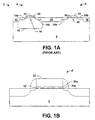
- Fig. 1A illustrates a conventional CMOS device 2 with PMOS and NMOS transistor devices 4 and 6, respectively, formed in or on a silicon substrate 8.
- Isolation structures 10 are formed to separate and provide electrical isolation of the individual devices 4 and 6 from other devices and from one another.
- the substrate 8 is lightly doped p-type silicon with an n-well 12 formed therein under the PMOS transistor 4.
- the PMOS device 4 includes two laterally spaced p-doped source/drain regions 14a and 14b with a channel region 16 located therebetween in the n-well 12.
- a gate is formed over the channel region 16 comprising an SiO 2 gate dielectric 20 overlying the channel 16 and a conductive polysilicon gate contact structure 22 formed over the gate dielectric 20.
- the NMOS device 6 includes two laterally spaced n-doped source/drain regions 24a and 24b outlying a channel region 26 in the substrate 8 (or alternatively a p-well region (not shown)) with a gate formed over the channel region 26 comprising an SiO 2 gate dielectric layer 30 and a polysilicon gate contact 32, where the gate dielectrics 20 and 30 may be patterned from the same oxide layer.
- the resistivity of the channel 26 may be controlled by the voltage applied to the gate contact 32, by which changing the gate voltage changes the amount of current through channel 26.
- the gate contact 32 and the channel 26 are separated by the SiO 2 gate dielectric 30, which is an insulator. Thus, little or no current flows between the gate contact 32 and the channel 26, although "tunneling" current is observed with thin dielectrics.
- the gate dielectric 30 allows the gate voltage at the contact 32 to induce an electric field in the channel 26, by which the channel resistance can be controlled by the applied gate voltage.
- MOSFET devices produce an output current proportional to the ratio of the width over the length of the channel, where the channel length is the physical distance between the source/drain regions ( e.g. , between regions 24a and 24b in the device 6) and the width runs perpendicular to the length ( e.g. , perpendicular to the page in Fig. 1A).
- scaling the NMOS device 6 to make the width narrower may reduce the device output current.
- this characteristic has been accommodated by decreasing the thickness of gate dielectric 30, thus bringing the gate contact 32 closer to the channel 26 for the device 6 of Fig. 1A.
- Making the gate dielectric layer 30 thinner has other effects, which may lead to performance tradeoffs, particularly where the gate dielectric 30 is SiO 2 .
- a thin SiO 2 gate dielectric 30 provides a poor diffusion barrier to dopants, for example, causing high boron dopant penetration into the underlying channel region 26 during fabrication of the source/drain regions 24a and 24b.
- such high-k dielectrics are typically deposited directly over a silicon substrate to form a gate dielectric layer of about 50 Angstroms.
- the performance and reliability of the resulting transistors is dependent upon the quality of the interface between the high-k dielectric material and the underlying silicon.
- a high-k gate dielectric material 30a is used to form a gate dielectric layer 30' in an NMOS device 6'.
- a conductive polysilicon gate contact structure 32' is then formed over the high-k dielectric layer 30a.
- the alternative gate dielectric materials explored thus far typically include oxygen components, and are often deposited using deposition techniques, such as chemical vapor deposition (CVD), atomic layer deposition (ALD), or physical vapor deposition (PVD) processes, that use oxidizing reactants.
- CVD chemical vapor deposition
- ALD atomic layer deposition
- PVD physical vapor deposition
- the upper surface of the silicon substrate 8 oxidizes, forming an unintended low quality, low-k oxide layer 30b between the substrate 8 and the high-k material 30a.
- the presence of this interfacial oxide layer 30b increases the effective oxide thickness, reducing the effectiveness of the alternative gate dielectric approach.
- the interface 30b generally has unsatisfied bonds that act as interface charging centers, causing interface states.
- the high density of such interface states in the low quality oxide 30b results in carrier mobility degradation in operation of the transistor 6', where the higher the density of the interface states, the more the resulting mobility degradation.
- lower quality oxides may also suffer from issues related to, among other things, charge scattering, charge trapping, fixed charge, density of interface state (D it ), carrier mobility, etc.
- low charge scattering may be related to a high mobility type of oxide.
- Carriers in a channel created with a gate oxide of low charge scattering may have high mobility, for example.
- non-thermal oxides e.g., UV-ozone oxide, UV-O 3 or chemical oxides
- Such non-thermal oxides are typically grown at low temperatures. While these non-thermal oxides are generally better than unintended thermal oxides formed during high-k growth ( e.g. , layer 30b in Fig. 1B), there is a need for better mobility than that which can be achieved with non-thermal oxides. Growing oxides at higher temperatures produces higher quality oxides, but the oxide growth rate is difficult to control as the oxidation occurs rapidly at higher temperatures.
- the invention relates to methods for forming a high quality thin interface oxide layer suitable for use with high-k gate dielectrics in the manufacture of semiconductor devices.
- the layer can be grown to thicknesses of about 10 Angstroms or less at temperatures of about 850 degrees Celsius or more.
- the rate of growth of the interface oxide layer is controllable to allow the layer to be grown at higher temperatures, which in turn facilitates production of a higher quality layer.
- the growth rate is controlled by governing the partial pressure of a reducing agent that simultaneously counteracts the oxidation or growth of the layer.
- the partial pressure is the fraction of an agent times the total pressure.
- a method of fabricating a transistor gate structure in a semiconductor device includes growing an interface oxide layer to a thickness of about 10 Angstroms or less over a semiconductor body.
- the layer is grown using an ambient comprising oxygen and a reducing agent.
- the presence of oxidizer and a reducer in an appropriate mixture leads to a concurrent oxidation and reduction of the oxide such that the oxide is grown at a rate of between about 20 to 55 Angstroms per minute at a temperature of about 850 degrees Celsius or more.
- the method also includes forming a high-k dielectric layer over the interface oxide layer, forming a gate contact layer over the high-k dielectric layer and then patterning the gate contact layer, the high-k dielectric layer, and the interface oxide layer to form a transistor gate structure.
- a transistor gate structure suitable for implementation in a semiconductor device.
- the structure includes an interface oxide layer formed over a semiconductor body; a high-k dielectric layer formed over the interface oxide layer and a gate contact layer formed over the high-k dielectric layer.
- the gate contact layer, the high-k dielectric layer, and the interface oxide layer are patterned to form the transistor gate structure.
- An oxidant comprising an oxygen containing molecule and a reducing agent is utilized to grow the interface oxide layer to a thickness of about 10 Angstroms or less.
- the oxidant presence of oxidizer and reducer in an appropriate mixture leads to a rate of between about 20 to 55 Angstroms per minute at a temperature of about 850 degrees Celsius or more.
- the invention relates to formation of ultra thin interface oxides suitable for implementation in gate structures in semiconductor devices, and more particularly to growing the interface oxides at high temperatures while controlling the rate of growth of the oxides (which traditionally speeds up growth rates).
- the present invention pertains to methods for forming high quality thin interface oxide layers suitable for use with high-k gate dielectrics in the manufacture of semiconductor devices.
- the layers can be grown to thicknesses of about 10 Angstroms or less at relatively high temperatures of about 850 degrees Celsius or more.
- the rate of growth of the layers is controllable to allow the layers to be grown at higher temperatures, which facilitates production of higher quality layers.
- the higher quality layers facilitate production of better performing and more reliable resulting devices.
- the growth rate is controlled by governing the partial pressure of a reducing agent that concurrently counteracts the oxidation or growth of the layers, where the layers are grown by exposure to oxygen contained within an oxidant that also includes the reducing agent.
- a flow diagram illustrates an exemplary method 200 for processing semiconductor devices, including fabrication of transistor gate structures in accordance with the present invention.
- the method 200 is illustrated and described herein as a series of acts or events, it will be appreciated that the present invention is not limited by the illustrated ordering of such acts or events. For example, some acts may occur in different orders and/or concurrently with other acts or events apart from those illustrated and/or described herein, in accordance with the invention. In addition, not all illustrated steps may be required to implement a methodology in accordance with the present invention. In addition, the methods according to the present invention may be implemented in association with the formation and/or processing of structures illustrated and described herein as well as in association with other structures not illustrated.
- the method 200 comprises forming isolation structures at 204, such as STI or LOCOS oxide isolation structures in a semiconductor body.
- isolation structures such as STI or LOCOS oxide isolation structures in a semiconductor body.
- one or more wells e.g., n-wells and/or p-wells
- gate fabrication begins, where a wet clean or a HF deglaze may be optionally performed at 210 to clean a top surface of the semiconductor body before growing the high quality interface oxide layer.
- the precleaning at 210 may be employed for removal of any thin dielectric layers from the silicon body, such as silicon oxide (SiO), silicon nitride (SiN), or silicon oxynitride (SiON).
- wet cleaning operations can be performed at 210, or a dilute HF solution may be employed to deglaze the semiconductor body.
- a dilute HF solution may be employed to deglaze the semiconductor body.
- a dilute HF solution involves dipping the semiconductor in a 1:100 volume dilution of 49% HF at room temperature for a duration that is adequate to completely remove and SiO from the surface.
- a dry process is employed comprising a mixture of anhydrous HF and isopropyl-alcohol to remove SiO.
- a high quality ultra-thin (e.g., 10 Angstroms or less) interface oxide layer is grown over the semiconductor body using an oxidant comprising oxygen and a reducing agent.
- the semiconductor body generally comprises silicon, and the oxygen reacts with the silicon to form the oxide interface layer (e.g. , silicon dioxide (SiO 2 )).
- the reducing agent simultaneously etches the oxide interface layer as the layer is grown ( e.g., via the presence of the oxygen in the ambient oxidant).
- the concurrent oxidation and reduction of the oxide interface layer slows the resulting effective growth rate of the layer allowing it to be grown in a controllable manner ( e.g. , to achieve a desired thickness and/or level of uniformity).
- the concurrent oxidation and reduction also permits the layer to be formed under higher temperatures (e.g. , about 850 degrees Celsius or more). Growing the oxide interface layer at higher temperatures yields higher quality oxides, that in turn facilitates production of better and more reliable resulting products.
- a curve 300 of the growth rate (y-axis) of the oxide interface layer versus a partial pressure of the reducing agent in the gas phase (x-axis) is depicted.
- the partial pressure is the fraction of a reducing agent in the gas phase times the total pressure (e.g. , in a processing chamber wherein the gases are contained).
- the reducing agent is hydrogen, and a balance of nitrous oxide (N 2 O) is also present.
- the reducing agent can comprise any suitable number of elements, either alone or in combination, such as hydrochloric acid (HCl), for example, that counteract the oxidation to reduce the rate of oxide growth.
- HCl hydrochloric acid
- nitrous oxide may be utilized as the oxidizing agent, for purposes of the present invention, the oxidizing agent can comprise any suitable number of elements or molecules, either alone or in combination, such oxygen or nitric oxide for example, that can oxidize silicon.
- the layer of silicon dioxide (SiO 2 ) is generated under a total pressure of about 12.5 Torr at a temperature of about 1050 degrees Celsius. It will be appreciated, however, that these parameters may be varied to achieve different results.
- the SiO 2 oxide interface layer can be grown under a pressure of between about 1 mTorr to 100 Torr to alter the growth rate where low pressure (even ⁇ 1 mTorr) is advantageous to retard the growth rate.
- the interface oxide layer formed at 212 may operate as a high quality nucleation layer for the high-k deposition at 214.
- the high-k dielectric material can be applied in any suitable manner, such as with spin-on techniques, sputtering techniques (e.g. , magnetron or ion beam sputtering), growth and/or deposition techniques, such as chemical vapor deposition (CVD) or atomic layer deposition (ALD), for example.
- the high-k dielectric material can be formed to a thickness of about 1 nanometers or more, and can have an equivalent oxide thickness (EOT) of about 1 nanometers or less, for example.
- the high-k dielectric material generally comprises a material having a dielectric constant higher than about 3.9 ( e.g. , higher than silicon dioxide (SiO 2 )).
- high-k dielectric materials include, but are not limited to binary metal oxides including aluminum oxide (Al 2 O 3 ), zirconium oxide (ZrO 2 ), hafnium oxide (HfO 2 ), lanthanum oxide (La 2 O 3 ), yttrium oxide (Y 2 O 3 ), titanium oxide (TiO 2 ), as well as their silicates and aluminates; metal oxynitrides including aluminum oxynitride (AION), zirconium oxynitride (ZrON), hafnium oxynitride (HfON), lanthanum oxynitride (LaON), yttrium oxynitride (YON), as well as their silicates and aluminates such as ZrSiON, HfSiON, LaSiON, YSiON etc.; and perovskite-type oxides including a titanate system material such as barium titanate, strontium titanate, barium strontium titanate,
- a conductive metal or polycrystalline silicon (polysilicon) gate contact layer is then formed over the high-k dielectric layer at 216 ( e.g. , via sputtering, deposition, growth techniques, etc.).
- the gate electrode layer generally includes polysilicon, and can be formed to a thickness of about 100 nanometers, for example.
- the gate electrode layer ultimately yields a contact that provides a structure for applying a voltage to the transistor or otherwise biasing the transistor.
- the gate contact layer, the high-k dielectric layer, and the interface oxide layer are then patterned to form a gate structure at 218.
- the transistor gate structure thus comprises a gate electrode, a high-k gate dielectric and a thin interface oxide layer.
- the layers can be patterned in any suitable manner to form the gate structure, such as by etching, for example.
- the gate fabrication then ends at 220.
- source/drain regions of the semiconductor body are provided with appropriate n or p type dopants through implantation or diffusion, and interconnect processing is performed at 224 according to known interconnect techniques, before the method 200 ends at 226.
- the polysilicon gate contact layer may be initially patterned without patterning the gate dielectric and interface layers, where the source/drain regions are implanted through the gate dielectric and interface layers, and the high-k dielectric and interface oxide layers are patterned later.
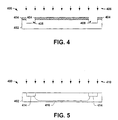
- the device 400 comprises a wafer having a semiconductor body 402 therein, such as a silicon substrate or other semiconductor substrate, or a layer of silicon or other semiconductor deposited over an insulator in an SOl device wafer.
- the semiconductor body 402 is a lightly doped p-type silicon substrate.
- semiconductor body as used herein can include a base semiconductor wafer and any epitaxial layers or other type semiconductor layers formed there over or associated therewith.
- isolation structures e.g., SiO 2 field oxide (FOX) or shallow trench isolation (STI) structures
- An isolation mask 404 is formed over the device 400 in Fig. 4 and a trench etch process 406 is performed to form isolation trenches 408 in isolation regions of the semiconductor body 402.
- the trenches 408 are then filled in Fig. 5 with dielectric material via a deposition process 410 and the device 400 is planarized via a CMP process (not shown) to leave STI type dielectric isolation structures 414, for example, SiO 2 .
- One or more p and/or n-type wells are then formed in the semiconductor body 402, including an n-well 416, as illustrated in Fig. 5, and an optional wet clean or HF deglaze operation (not shown) may be performed to clean the top surface of the semiconductor body 402.
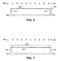
- gate fabrication processing begins with the growth of an ultra-thin high quality interface oxide layer 418 over the semiconductor body 402 via a high temperature oxidation process 420.
- the oxide interface layer 418 is grown to a thickness 422 of about 10 Angstroms or less, and generally comprises silicon ( e.g. , SiO 2 ).
- the duration of the oxidation process 420 can vary depending upon the equipment and/or tooling utilized.
- the rate of growth of the interface oxide layer 418 is controlled by regulating the partial pressure of a reducing agent to which the body 402 is exposed.
- the partial pressure is the fraction of an agent relative to the total pressure (e.g. , in a processing chamber containing these reactant gases and the body).
- the interface layer 418 is grown by exposing the semiconductor body 402 to the oxidant mixture which contains the oxygen and the reducing agent.
- the oxygen reacts with the body 402 to oxidize the body and establish the oxide interface layer 418.
- the reducing agent concurrently etches the oxide interface layer 418 as the layer is grown.
- the concurrent oxidation and reduction of the oxide interface layer slows the growth rate of the layer 418 allowing it to be grown in a controllable manner (e.g. , to achieve a desired thickness and/or level of uniformity).
- the reducing agent can be, for example, hydrogen and/or any other suitable element, such as hydrochloric acid (HCl), for example, that, alone or in combination, counteracts the oxidation process to reduce the rate of oxide growth.
- the hydrogen in the gas phase is below about 2 Torr (e.g. , between about 1 and 2 Torr)
- the hydrogen reacts with the oxygen to form water vapor (H 2 O), which facilitates an increase in the oxidation rate from about 35 to about 55 Angstroms/minute.
- H 2 O water vapor
- the partial pressure of hydrogen exceeds about 6 Torr, the hydrogen combines with the oxygen to a lesser and lesser degree, so that the "wet" oxidation ceases, and the excess hydrogen begins to act as an etchant to slow the rate of growth of the oxide interface layer 418.
- the partial pressure of hydrogen increases (e.g.
- the growth rate of the oxide layer is reduced further and further (e.g. , from about 55 to about 20 Angstroms/minute). While particular values for different parameters (e.g. , temperature, pressure) have been discussed herein, it will be appreciated that these values may be varied to achieve different results.
- the simultaneous oxidation and reduction permits the interface layer 418 to be formed under higher temperatures due to the enhanced control of growth rate.
- Growing the oxide interface layer 418 at higher temperatures yields higher quality oxides, which in turn facilitates production of better and more reliable resulting products.
- atoms e.g. , of oxygen
- the higher quality oxide possesses fewer dangling bonds (e.g. , that are not fulfilled by oxygen) at an interface of the body 402 with the oxide interface layer 418.
- lower temperatures e.g. , conventionally below about 850 degrees Celsius
- more defects are created because there is less atomic mobility resulting in more "frozen-in" defects.
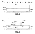
- a high-k dielectric layer 424 is formed over the interface oxide layer 418 via a deposition process 426 (e.g., CVD, ALD, or sputtering). It is to be appreciated that any one or more high-k dielectric materials can be utilized, either alone or in combination, to form the layer 424. Some examples of suitable high-k dielectric materials are set forth in Table 1 below.
- Dielectric Material Approximate Relative Permittivity (k) aluminum oxide (Al 2 O 3 ) 9-10 zirconium silicate 12 hafnium silicate 15 hafnium silicon oxynitride 16 hafnium silicon nitride 18 lanthanum oxide (La 2 O 3 ) 20-30 hafnium oxide (HfO 2 ) 40 zirconium oxide (ZrO 2 ) 25 cerium oxide (CeO 2 ) 26 bismuth silicon oxide (Bi 4 Si 2 O 12 ) 35-75 titanium dioxide (TiO 2 ) 30 tantalum oxide (Ta 2 O 5 ) 26 tungsten oxide (WO 3 ) 42 yttrium oxide (Y 2 O 3 ) 20 lanthanum aluminum oxide (LaAlO 3 ) 25 barium strontium titanate (Ba 1-x Sr x TiO 3 ) about 20-about 200 barium strontium oxide (Ba 1-x Sr x O 3 ) about 20-about 200 PbTiO 3 about
- Table 1 is not an exhaustive list of high-k dielectric materials and that other high-k materials may be available. It will be further appreciated that the k-values for both standard-k and high-k materials may vary to some degree depending on the exact nature of the dielectric material. Thus, for example, differences in purity, crystallinity and stoichiometry, may give rise to variations in the exact k-value determined for any particular dielectric material.
- the material when a material is referred to by a specific chemical name or formula, the material may include non-stoichiometric variations of the stoichiometrically exact formula identified by the chemical name.
- tantalum oxide when stoichiometrically exact, has the chemical formula Ta 2 O 5 , but may include variants of stoichiometric Ta 2 O 5 , which may be referred to as Ta x O y , in which either of x or y vary by a small amount.
- x may vary from about 1.5 to 2.5, and y may vary from about 4.5 to about 5.5.
- x may vary from about 1.75 to 2.25, and y may vary from about 4 to about 6.
- a gate contact layer 428 such as polysilicon (or other conductive gate electrode, such as metals, metal nitride and metal silicides) is then deposited over the high-k material 424 via a deposition process 430.
- the gate contact layer 428, the high-k dielectric layer 424, and the interface oxide layer 418 are patterned to form a transistor gate structure 432.
- Source/drain regions 434 are doped with p-type impurities on either side of a channel region 436 in the semiconductor body 402, and sidewall spacers 438 are formed along the sides of the patterned layers 418, 424, and 428 as illustrated in Fig. 9.
- interconnect processing (not shown) is performed to interconnect the illustrated MOS type transistor and other electrical components in the device 400.
Landscapes
- Chemical & Material Sciences (AREA)
- Chemical Kinetics & Catalysis (AREA)
- Engineering & Computer Science (AREA)
- Materials Engineering (AREA)
- Mechanical Engineering (AREA)
- Metallurgy (AREA)
- Organic Chemistry (AREA)
- Insulated Gate Type Field-Effect Transistor (AREA)
- Formation Of Insulating Films (AREA)
Abstract
Description
| Dielectric Material | Approximate Relative Permittivity (k) |
| aluminum oxide (Al2O3) | 9-10 |
| | 12 |
| hafnium silicate | 15 |
| | 16 |
| hafnium silicon nitride | 18 |
| lanthanum oxide (La2O3) | 20-30 |
| hafnium oxide (HfO2) | 40 |
| zirconium oxide (ZrO2) | 25 |
| cerium oxide (CeO2) | 26 |
| bismuth silicon oxide (Bi4Si2O12) | 35-75 |
| titanium dioxide (TiO2) | 30 |
| tantalum oxide (Ta2O5) | 26 |
| tungsten oxide (WO3) | 42 |
| yttrium oxide (Y2O3) | 20 |
| lanthanum aluminum oxide (LaAlO3) | 25 |
| barium strontium titanate (Ba1-xSrxTiO3) | about 20-about 200 |
| barium strontium oxide (Ba1-xSrxO3) | about 20-about 200 |
| PbTiO3 | about 20-about 200 |
| barium titanate (BaTiO3) | about 20-about 200 |
| strontium titanate SrTiO3 | about 20-about 200 |
| PbZrO3 | about 20-about 200 |
| PST (PbSCbxTa1-xO3) | 3000 |
| PZN (PbZnxNb1-xO3) | about 500-about 5000 |
| PZT (PbZrxTi1-xO3) | about 150-about 1000 |
| PMN (PbMgxNb1-xO3) | about 500-about 5000 |
Claims (10)
- A method of forming a high quality oxide layer suitable for use as an interface oxide layer between a high-k dielectric and an underlying substrate in a semiconductor device comprising:introducing an oxidant comprising oxygen and a reducing agent to a semiconductor body;growing the oxide layer over the semiconductor body with the oxidant; andconcurrently reducing the oxide layer with the reducing agent, where the concurrent growth and reduction facilitates growing the oxide layer at a controlled rate.
- The method of claim 1, wherein the growth rate is controlled to be between about 20-55 Angstroms per minute at a temperature of about 850°C or more.
- The method of claim 1 or 2, wherein the reducing agent comprises hydrogen.
- The method of any one of claims 1 to 3, wherein the reducing agent has a partial pressure between about 6 and 12 Torr.
- The method of any one of claims 1 to 4, wherein the reducing agent etches the oxide layer to reduce the rate of growth.
- The method of any one of claims 1 to 5, wherein the growth occurs under a pressure of between about 1 mTorr to 100 Torr.
- The method of claim 1, wherein the reducing agent comprises hydrochloric acid (HCl).
- The method of claim 3, wherein the oxidant further comprises at least one of nitrous oxide (N2O), oxygen (O2), carbon monoxide (CO) and carbon dioxide (CO2),
- The method of claim 1, wherein the growth occurs at a temperature from about 850 to about 1150 degrees Celsius.
- A transistor gate structure suitable for implementation in a semiconductor device, comprising:an interface oxide layer formed over a semiconductor body;a high-k dielectric layer formed over the interface oxide layer; anda gate contact layer formed over the high-k dielectric layer,
the gate contact layer, the high-k dielectric layer, and the interface oxide layer patterned to form the transistor gate structure,
the interface oxide layer grown to a thickness of about 10 Angstroms or less utilizing an oxidant comprising oxygen and a reducing agent, where the oxidant facilitating concurrent oxidation and reduction of the oxide to grow the oxide at a controlled rate.
Applications Claiming Priority (2)
| Application Number | Priority Date | Filing Date | Title |
|---|---|---|---|
| US367429 | 2003-02-13 | ||
| US10/367,429 US6852645B2 (en) | 2003-02-13 | 2003-02-13 | High temperature interface layer growth for high-k gate dielectric |
Publications (2)
| Publication Number | Publication Date |
|---|---|
| EP1450395A2 true EP1450395A2 (en) | 2004-08-25 |
| EP1450395A3 EP1450395A3 (en) | 2005-04-13 |
Family
ID=32736396
Family Applications (1)
| Application Number | Title | Priority Date | Filing Date |
|---|---|---|---|
| EP04100598A Withdrawn EP1450395A3 (en) | 2003-02-13 | 2004-02-13 | High temperature interface layer growth for high-K gate dielectric |
Country Status (3)
| Country | Link |
|---|---|
| US (2) | US6852645B2 (en) |
| EP (1) | EP1450395A3 (en) |
| JP (1) | JP2004247736A (en) |
Cited By (3)
| Publication number | Priority date | Publication date | Assignee | Title |
|---|---|---|---|---|
| DE102007063270A1 (en) * | 2007-12-31 | 2009-07-02 | Advanced Micro Devices, Inc., Sunnyvale | Reduction of the generation of charge trapping sites in gate dielectrics in MOS transistors by performing a hydrogen treatment |
| WO2009156954A1 (en) * | 2008-06-25 | 2009-12-30 | Nxp B.V. | Interfacial layer regrowth control in high-k gate structure for field effect transistor |
| CN103125014A (en) * | 2010-09-28 | 2013-05-29 | 国际商业机器公司 | Semiconductor device with a gate stack |
Families Citing this family (61)
| Publication number | Priority date | Publication date | Assignee | Title |
|---|---|---|---|---|
| US9418381B2 (en) * | 2000-04-14 | 2016-08-16 | Citigroup Credit Services, Inc. (USA) | Method and system for notifying customers of transaction opportunities |
| US8725632B2 (en) | 2000-01-13 | 2014-05-13 | Citicorp Development Center, Inc. | Method and system for conducting financial and non-financial transactions using a wireless device |
| US8346677B1 (en) | 2000-12-29 | 2013-01-01 | Citicorp Development Center, Inc. | Method and system for conducting commerce over a wireless communication network |
| US7068544B2 (en) * | 2001-08-30 | 2006-06-27 | Micron Technology, Inc. | Flash memory with low tunnel barrier interpoly insulators |
| US7589029B2 (en) | 2002-05-02 | 2009-09-15 | Micron Technology, Inc. | Atomic layer deposition and conversion |
| US7037863B2 (en) * | 2002-09-10 | 2006-05-02 | Samsung Electronics Co., Ltd. | Post thermal treatment methods of forming high dielectric layers over interfacial layers in integrated circuit devices |
| US7192892B2 (en) | 2003-03-04 | 2007-03-20 | Micron Technology, Inc. | Atomic layer deposited dielectric layers |
| US7135369B2 (en) | 2003-03-31 | 2006-11-14 | Micron Technology, Inc. | Atomic layer deposited ZrAlxOy dielectric layers including Zr4AlO9 |
| US7192824B2 (en) * | 2003-06-24 | 2007-03-20 | Micron Technology, Inc. | Lanthanide oxide / hafnium oxide dielectric layers |
| US20060011905A1 (en) * | 2003-06-26 | 2006-01-19 | Rj Mears, Llc | Semiconductor device comprising a superlattice dielectric interface layer |
| US7446002B2 (en) | 2003-06-26 | 2008-11-04 | Mears Technologies, Inc. | Method for making a semiconductor device comprising a superlattice dielectric interface layer |
| US6921691B1 (en) * | 2004-03-18 | 2005-07-26 | Infineon Technologies Ag | Transistor with dopant-bearing metal in source and drain |
| US20050276922A1 (en) * | 2004-06-10 | 2005-12-15 | Henry Bernhardt | Method of forming thin dielectric layers |
| US8178902B2 (en) | 2004-06-17 | 2012-05-15 | Infineon Technologies Ag | CMOS transistor with dual high-k gate dielectric and method of manufacture thereof |
| US8399934B2 (en) * | 2004-12-20 | 2013-03-19 | Infineon Technologies Ag | Transistor device |
| US7592678B2 (en) * | 2004-06-17 | 2009-09-22 | Infineon Technologies Ag | CMOS transistors with dual high-k gate dielectric and methods of manufacture thereof |
| US7560361B2 (en) * | 2004-08-12 | 2009-07-14 | International Business Machines Corporation | Method of forming gate stack for semiconductor electronic device |
| US7588988B2 (en) * | 2004-08-31 | 2009-09-15 | Micron Technology, Inc. | Method of forming apparatus having oxide films formed using atomic layer deposition |
| US7202562B2 (en) * | 2004-12-02 | 2007-04-10 | Micron Technology, Inc. | Integrated circuit cooling system and method |
| US7344934B2 (en) | 2004-12-06 | 2008-03-18 | Infineon Technologies Ag | CMOS transistor and method of manufacture thereof |
| US7235501B2 (en) | 2004-12-13 | 2007-06-26 | Micron Technology, Inc. | Lanthanum hafnium oxide dielectrics |
| KR20060072498A (en) * | 2004-12-23 | 2006-06-28 | 동부일렉트로닉스 주식회사 | Semiconductor device and its manufacturing method |
| US7560395B2 (en) | 2005-01-05 | 2009-07-14 | Micron Technology, Inc. | Atomic layer deposited hafnium tantalum oxide dielectrics |
| US20060151846A1 (en) * | 2005-01-13 | 2006-07-13 | International Business Machines Corporation | Method of forming HfSiN metal for n-FET applications |
| US7498229B1 (en) * | 2005-02-09 | 2009-03-03 | Translucent, Inc. | Transistor and in-situ fabrication process |
| US7399666B2 (en) * | 2005-02-15 | 2008-07-15 | Micron Technology, Inc. | Atomic layer deposition of Zr3N4/ZrO2 films as gate dielectrics |
| US7160781B2 (en) | 2005-03-21 | 2007-01-09 | Infineon Technologies Ag | Transistor device and methods of manufacture thereof |
| US7687409B2 (en) | 2005-03-29 | 2010-03-30 | Micron Technology, Inc. | Atomic layer deposited titanium silicon oxide films |
| US7365027B2 (en) | 2005-03-29 | 2008-04-29 | Micron Technology, Inc. | ALD of amorphous lanthanide doped TiOx films |
| US7361538B2 (en) * | 2005-04-14 | 2008-04-22 | Infineon Technologies Ag | Transistors and methods of manufacture thereof |
| US7390756B2 (en) * | 2005-04-28 | 2008-06-24 | Micron Technology, Inc. | Atomic layer deposited zirconium silicon oxide films |
| US7662729B2 (en) | 2005-04-28 | 2010-02-16 | Micron Technology, Inc. | Atomic layer deposition of a ruthenium layer to a lanthanide oxide dielectric layer |
| US7354872B2 (en) * | 2005-05-26 | 2008-04-08 | International Business Machines Corporation | Hi-K dielectric layer deposition methods |
| US7927948B2 (en) | 2005-07-20 | 2011-04-19 | Micron Technology, Inc. | Devices with nanocrystals and methods of formation |
| US7410910B2 (en) * | 2005-08-31 | 2008-08-12 | Micron Technology, Inc. | Lanthanum aluminum oxynitride dielectric films |
| US8188551B2 (en) * | 2005-09-30 | 2012-05-29 | Infineon Technologies Ag | Semiconductor devices and methods of manufacture thereof |
| US20070052036A1 (en) * | 2005-09-02 | 2007-03-08 | Hongfa Luan | Transistors and methods of manufacture thereof |
| US7462538B2 (en) * | 2005-11-15 | 2008-12-09 | Infineon Technologies Ag | Methods of manufacturing multiple gate CMOS transistors having different gate dielectric materials |
| US7495290B2 (en) * | 2005-12-14 | 2009-02-24 | Infineon Technologies Ag | Semiconductor devices and methods of manufacture thereof |
| US7510943B2 (en) * | 2005-12-16 | 2009-03-31 | Infineon Technologies Ag | Semiconductor devices and methods of manufacture thereof |
| US7972974B2 (en) | 2006-01-10 | 2011-07-05 | Micron Technology, Inc. | Gallium lanthanide oxide films |
| US7709402B2 (en) | 2006-02-16 | 2010-05-04 | Micron Technology, Inc. | Conductive layers for hafnium silicon oxynitride films |
| JP4282691B2 (en) * | 2006-06-07 | 2009-06-24 | 株式会社東芝 | Semiconductor device |
| US7544604B2 (en) * | 2006-08-31 | 2009-06-09 | Micron Technology, Inc. | Tantalum lanthanide oxynitride films |
| US7776765B2 (en) | 2006-08-31 | 2010-08-17 | Micron Technology, Inc. | Tantalum silicon oxynitride high-k dielectrics and metal gates |
| US7759747B2 (en) | 2006-08-31 | 2010-07-20 | Micron Technology, Inc. | Tantalum aluminum oxynitride high-κ dielectric |
| US20080057659A1 (en) * | 2006-08-31 | 2008-03-06 | Micron Technology, Inc. | Hafnium aluminium oxynitride high-K dielectric and metal gates |
| US7432548B2 (en) * | 2006-08-31 | 2008-10-07 | Micron Technology, Inc. | Silicon lanthanide oxynitride films |
| US7563730B2 (en) | 2006-08-31 | 2009-07-21 | Micron Technology, Inc. | Hafnium lanthanide oxynitride films |
| US7605030B2 (en) | 2006-08-31 | 2009-10-20 | Micron Technology, Inc. | Hafnium tantalum oxynitride high-k dielectric and metal gates |
| US20080237694A1 (en) * | 2007-03-27 | 2008-10-02 | Michael Specht | Integrated circuit, cell, cell arrangement, method for manufacturing an integrated circuit, method for manufacturing a cell, memory module |
| US20080315206A1 (en) * | 2007-06-19 | 2008-12-25 | Herner S Brad | Highly Scalable Thin Film Transistor |
| US20090142899A1 (en) * | 2007-12-04 | 2009-06-04 | Jensen Jacob M | Interfacial layer for hafnium-based high-k/metal gate transistors |
| JP5104373B2 (en) * | 2008-02-14 | 2012-12-19 | 日本ゼオン株式会社 | Production method of retardation plate |
| US7947549B2 (en) * | 2008-02-26 | 2011-05-24 | International Business Machines Corporation | Gate effective-workfunction modification for CMOS |
| US20120309206A1 (en) * | 2011-04-22 | 2012-12-06 | Applied Materials, Inc. | Stoichiometry Control Of Transition Metal Oxides In Thin Films |
| JP6088804B2 (en) * | 2012-11-16 | 2017-03-01 | 富士電機株式会社 | Silicon carbide semiconductor device and method for manufacturing silicon carbide semiconductor device |
| US9887100B2 (en) * | 2014-10-03 | 2018-02-06 | Taiwan Semiconductor Manufacturing Company, Ltd. | Methods of forming semiconductor devices and structures thereof |
| US10672886B2 (en) * | 2017-08-31 | 2020-06-02 | Taiwan Semiconductor Manufacturing Company, Ltd. | Structure and method for high-k metal gate |
| JP7788870B2 (en) * | 2022-01-19 | 2025-12-19 | 東京エレクトロン株式会社 | Film formation method and tungsten film |
| JP7788869B2 (en) * | 2022-01-19 | 2025-12-19 | 東京エレクトロン株式会社 | Stress reduction methods |
Family Cites Families (16)
| Publication number | Priority date | Publication date | Assignee | Title |
|---|---|---|---|---|
| JPH02303131A (en) * | 1989-05-18 | 1990-12-17 | Oki Electric Ind Co Ltd | Insulating film formation method |
| EP0417457A3 (en) * | 1989-08-11 | 1991-07-03 | Seiko Instruments Inc. | Method of producing field effect transistor |
| JP2643833B2 (en) * | 1994-05-30 | 1997-08-20 | 日本電気株式会社 | Semiconductor memory device and method of manufacturing the same |
| US6320238B1 (en) * | 1996-12-23 | 2001-11-20 | Agere Systems Guardian Corp. | Gate structure for integrated circuit fabrication |
| US6037273A (en) * | 1997-07-11 | 2000-03-14 | Applied Materials, Inc. | Method and apparatus for insitu vapor generation |
| US6352941B1 (en) * | 1998-08-26 | 2002-03-05 | Texas Instruments Incorporated | Controllable oxidation technique for high quality ultrathin gate oxide formation |
| US6214736B1 (en) | 1998-10-15 | 2001-04-10 | Texas Instruments Incorporated | Silicon processing method |
| US6514879B2 (en) * | 1999-12-17 | 2003-02-04 | Intel Corporation | Method and apparatus for dry/catalytic-wet steam oxidation of silicon |
| US6448127B1 (en) * | 2000-01-14 | 2002-09-10 | Advanced Micro Devices, Inc. | Process for formation of ultra-thin base oxide in high k/oxide stack gate dielectrics of mosfets |
| US6492283B2 (en) * | 2000-02-22 | 2002-12-10 | Asm Microchemistry Oy | Method of forming ultrathin oxide layer |
| KR100560867B1 (en) * | 2000-05-02 | 2006-03-13 | 동경 엘렉트론 주식회사 | Oxidation Method and Oxidation System |
| US6638877B2 (en) * | 2000-11-03 | 2003-10-28 | Texas Instruments Incorporated | Ultra-thin SiO2using N2O as the oxidant |
| JP4104834B2 (en) * | 2001-04-13 | 2008-06-18 | 株式会社東芝 | Manufacturing method of MIS field effect transistor |
| US6806145B2 (en) * | 2001-08-31 | 2004-10-19 | Asm International, N.V. | Low temperature method of forming a gate stack with a high k layer deposited over an interfacial oxide layer |
| US6706581B1 (en) * | 2002-10-29 | 2004-03-16 | Taiwan Semiconductor Manufacturing Company | Dual gate dielectric scheme: SiON for high performance devices and high k for low power devices |
| US6716695B1 (en) * | 2002-12-20 | 2004-04-06 | Texas Instruments Incorporated | Semiconductor with a nitrided silicon gate oxide and method |
-
2003
- 2003-02-13 US US10/367,429 patent/US6852645B2/en not_active Expired - Lifetime
-
2004
- 2004-02-12 JP JP2004034537A patent/JP2004247736A/en active Pending
- 2004-02-13 EP EP04100598A patent/EP1450395A3/en not_active Withdrawn
- 2004-06-29 US US10/879,292 patent/US20040238904A1/en not_active Abandoned
Cited By (7)
| Publication number | Priority date | Publication date | Assignee | Title |
|---|---|---|---|---|
| DE102007063270A1 (en) * | 2007-12-31 | 2009-07-02 | Advanced Micro Devices, Inc., Sunnyvale | Reduction of the generation of charge trapping sites in gate dielectrics in MOS transistors by performing a hydrogen treatment |
| DE102007063270B4 (en) * | 2007-12-31 | 2011-06-01 | Amd Fab 36 Limited Liability Company & Co. Kg | A method of reducing the generation of charge trapping sites in gate dielectrics in MOS transistors by performing a hydrogen treatment |
| US8119461B2 (en) | 2007-12-31 | 2012-02-21 | Globalfoundries Inc. | Reducing the creation of charge traps at gate dielectrics in MOS transistors by performing a hydrogen treatment |
| WO2009156954A1 (en) * | 2008-06-25 | 2009-12-30 | Nxp B.V. | Interfacial layer regrowth control in high-k gate structure for field effect transistor |
| US8716812B2 (en) | 2008-06-25 | 2014-05-06 | Nxp B.V. | Interfacial layer regrowth control in high-K gate structure for field effect transistor |
| CN103125014A (en) * | 2010-09-28 | 2013-05-29 | 国际商业机器公司 | Semiconductor device with a gate stack |
| CN103125014B (en) * | 2010-09-28 | 2015-09-23 | 国际商业机器公司 | There is the semiconductor device of gate stack |
Also Published As
| Publication number | Publication date |
|---|---|
| JP2004247736A (en) | 2004-09-02 |
| EP1450395A3 (en) | 2005-04-13 |
| US20040238904A1 (en) | 2004-12-02 |
| US6852645B2 (en) | 2005-02-08 |
| US20040161883A1 (en) | 2004-08-19 |
Similar Documents
| Publication | Publication Date | Title |
|---|---|---|
| US6852645B2 (en) | High temperature interface layer growth for high-k gate dielectric | |
| US20040126944A1 (en) | Methods for forming interfacial layer for deposition of high-k dielectrics | |
| US7282773B2 (en) | Semiconductor device with high-k dielectric layer | |
| US7138680B2 (en) | Memory device with floating gate stack | |
| US7135361B2 (en) | Method for fabricating transistor gate structures and gate dielectrics thereof | |
| US6703277B1 (en) | Reducing agent for high-K gate dielectric parasitic interfacial layer | |
| US6682973B1 (en) | Formation of well-controlled thin SiO, SiN, SiON layer for multilayer high-K dielectric applications | |
| US6849925B1 (en) | Preparation of composite high-K/standard-K dielectrics for semiconductor devices | |
| US6809370B1 (en) | High-k gate dielectric with uniform nitrogen profile and methods for making the same | |
| US6559014B1 (en) | Preparation of composite high-K / standard-K dielectrics for semiconductor devices | |
| US6696332B2 (en) | Bilayer deposition to avoid unwanted interfacial reactions during high K gate dielectric processing | |
| US6790755B2 (en) | Preparation of stack high-K gate dielectrics with nitrided layer | |
| US6762114B1 (en) | Methods for transistor gate fabrication and for reducing high-k gate dielectric roughness | |
| US7858459B2 (en) | Work function adjustment with the implant of lanthanides | |
| US7091119B2 (en) | Encapsulated MOS transistor gate structures and methods for making the same | |
| TWI334157B (en) | Semiconductor device and method for manufacturing semiconductor device | |
| CN100490176C (en) | Semiconductor device and method for manufacturing the same | |
| US7807522B2 (en) | Lanthanide series metal implant to control work function of metal gate electrodes | |
| US20080203500A1 (en) | Semiconductor device and production method therefor | |
| JP4489368B2 (en) | Semiconductor device and manufacturing method thereof | |
| US7045431B2 (en) | Method for integrating high-k dielectrics in transistor devices | |
| US8058122B2 (en) | Formation of metal gate electrode using rare earth alloy incorporated into mid gap metal | |
| US20050142715A1 (en) | Semiconductor device with high dielectric constant insulator and its manufacture | |
| US6762454B1 (en) | Stacked polysilicon layer for boron penetration inhibition | |
| US12191377B2 (en) | Method for forming a semiconductor structure |
Legal Events
| Date | Code | Title | Description |
|---|---|---|---|
| PUAI | Public reference made under article 153(3) epc to a published international application that has entered the european phase |
Free format text: ORIGINAL CODE: 0009012 |
|
| AK | Designated contracting states |
Kind code of ref document: A2 Designated state(s): AT BE BG CH CY CZ DE DK EE ES FI FR GB GR HU IE IT LI LU MC NL PT RO SE SI SK TR |
|
| AX | Request for extension of the european patent |
Extension state: AL LT LV MK |
|
| PUAL | Search report despatched |
Free format text: ORIGINAL CODE: 0009013 |
|
| AK | Designated contracting states |
Kind code of ref document: A3 Designated state(s): AT BE BG CH CY CZ DE DK EE ES FI FR GB GR HU IE IT LI LU MC NL PT RO SE SI SK TR |
|
| AX | Request for extension of the european patent |
Extension state: AL LT LV MK |
|
| RIC1 | Information provided on ipc code assigned before grant |
Ipc: 7H 01L 29/51 B Ipc: 7C 23C 16/40 B Ipc: 7H 01L 21/28 B Ipc: 7H 01L 21/316 A |
|
| 17P | Request for examination filed |
Effective date: 20051013 |
|
| AKX | Designation fees paid |
Designated state(s): DE FR GB |
|
| 17Q | First examination report despatched |
Effective date: 20170105 |
|
| STAA | Information on the status of an ep patent application or granted ep patent |
Free format text: STATUS: THE APPLICATION IS DEEMED TO BE WITHDRAWN |
|
| 18D | Application deemed to be withdrawn |
Effective date: 20170516 |