EP1449403B1 - Optische raumschaltmatrix - Google Patents
Optische raumschaltmatrix Download PDFInfo
- Publication number
- EP1449403B1 EP1449403B1 EP01995682A EP01995682A EP1449403B1 EP 1449403 B1 EP1449403 B1 EP 1449403B1 EP 01995682 A EP01995682 A EP 01995682A EP 01995682 A EP01995682 A EP 01995682A EP 1449403 B1 EP1449403 B1 EP 1449403B1
- Authority
- EP
- European Patent Office
- Prior art keywords
- matrix
- optical
- port
- acousto
- optical switch
- Prior art date
- Legal status (The legal status is an assumption and is not a legal conclusion. Google has not performed a legal analysis and makes no representation as to the accuracy of the status listed.)
- Expired - Lifetime
Links
Images



Classifications
-
- H—ELECTRICITY
- H04—ELECTRIC COMMUNICATION TECHNIQUE
- H04Q—SELECTING
- H04Q11/00—Selecting arrangements for multiplex systems
- H04Q11/0001—Selecting arrangements for multiplex systems using optical switching
- H04Q11/0005—Switch and router aspects
-
- G—PHYSICS
- G02—OPTICS
- G02B—OPTICAL ELEMENTS, SYSTEMS OR APPARATUS
- G02B6/00—Light guides; Structural details of arrangements comprising light guides and other optical elements, e.g. couplings
- G02B6/24—Coupling light guides
- G02B6/26—Optical coupling means
- G02B6/35—Optical coupling means having switching means
- G02B6/354—Switching arrangements, i.e. number of input/output ports and interconnection types
- G02B6/3542—Non-blocking switch, e.g. with multiple potential paths between multiple inputs and outputs, the establishment of one switching path not preventing the establishment of further switching paths
-
- G—PHYSICS
- G02—OPTICS
- G02B—OPTICAL ELEMENTS, SYSTEMS OR APPARATUS
- G02B6/00—Light guides; Structural details of arrangements comprising light guides and other optical elements, e.g. couplings
- G02B6/24—Coupling light guides
- G02B6/26—Optical coupling means
- G02B6/35—Optical coupling means having switching means
- G02B6/354—Switching arrangements, i.e. number of input/output ports and interconnection types
- G02B6/3544—2D constellations, i.e. with switching elements and switched beams located in a plane
- G02B6/3546—NxM switch, i.e. a regular array of switches elements of matrix type constellation
-
- G—PHYSICS
- G02—OPTICS
- G02B—OPTICAL ELEMENTS, SYSTEMS OR APPARATUS
- G02B6/00—Light guides; Structural details of arrangements comprising light guides and other optical elements, e.g. couplings
- G02B6/24—Coupling light guides
- G02B6/26—Optical coupling means
- G02B6/35—Optical coupling means having switching means
- G02B6/354—Switching arrangements, i.e. number of input/output ports and interconnection types
- G02B6/356—Switching arrangements, i.e. number of input/output ports and interconnection types in an optical cross-connect device, e.g. routing and switching aspects of interconnecting different paths propagating different wavelengths to (re)configure the various input and output links
-
- G—PHYSICS
- G02—OPTICS
- G02B—OPTICAL ELEMENTS, SYSTEMS OR APPARATUS
- G02B6/00—Light guides; Structural details of arrangements comprising light guides and other optical elements, e.g. couplings
- G02B6/24—Coupling light guides
- G02B6/26—Optical coupling means
- G02B6/35—Optical coupling means having switching means
- G02B6/3564—Mechanical details of the actuation mechanism associated with the moving element or mounting mechanism details
- G02B6/3568—Mechanical details of the actuation mechanism associated with the moving element or mounting mechanism details characterised by the actuating force
- G02B6/3578—Piezoelectric force
-
- G—PHYSICS
- G02—OPTICS
- G02F—OPTICAL DEVICES OR ARRANGEMENTS FOR THE CONTROL OF LIGHT BY MODIFICATION OF THE OPTICAL PROPERTIES OF THE MEDIA OF THE ELEMENTS INVOLVED THEREIN; NON-LINEAR OPTICS; FREQUENCY-CHANGING OF LIGHT; OPTICAL LOGIC ELEMENTS; OPTICAL ANALOGUE/DIGITAL CONVERTERS
- G02F1/00—Devices or arrangements for the control of the intensity, colour, phase, polarisation or direction of light arriving from an independent light source, e.g. switching, gating or modulating; Non-linear optics
- G02F1/29—Devices or arrangements for the control of the intensity, colour, phase, polarisation or direction of light arriving from an independent light source, e.g. switching, gating or modulating; Non-linear optics for the control of the position or the direction of light beams, i.e. deflection
- G02F1/33—Acousto-optical deflection devices
-
- H—ELECTRICITY
- H04—ELECTRIC COMMUNICATION TECHNIQUE
- H04Q—SELECTING
- H04Q11/00—Selecting arrangements for multiplex systems
- H04Q11/0001—Selecting arrangements for multiplex systems using optical switching
- H04Q11/0005—Switch and router aspects
- H04Q2011/0007—Construction
- H04Q2011/0024—Construction using space switching
-
- H—ELECTRICITY
- H04—ELECTRIC COMMUNICATION TECHNIQUE
- H04Q—SELECTING
- H04Q11/00—Selecting arrangements for multiplex systems
- H04Q11/0001—Selecting arrangements for multiplex systems using optical switching
- H04Q11/0005—Switch and router aspects
- H04Q2011/0007—Construction
- H04Q2011/0035—Construction using miscellaneous components, e.g. circulator, polarisation, acousto/thermo optical
-
- H—ELECTRICITY
- H04—ELECTRIC COMMUNICATION TECHNIQUE
- H04Q—SELECTING
- H04Q11/00—Selecting arrangements for multiplex systems
- H04Q11/0001—Selecting arrangements for multiplex systems using optical switching
- H04Q11/0005—Switch and router aspects
- H04Q2011/0052—Interconnection of switches
- H04Q2011/0058—Crossbar; Matrix
Definitions
- the present invention relates to an acousto-optical space-switching matrix.
- the present invention relates to an optical spatial switching matrix comprising N input ports and M output ports, in which it is possible to switch an optical beam from any of the input ports to any of the output ports.
- WO 00/76252 discloses a matrix comprising add/drop switches comprising each a polarization beamsplitter and polarization controllers in front of each input path to the polarization beamsplitter.
- Each polarization beamsplitter operates by splitting an incoming beam into its polarization components, specifically the horizontal component p and the vertical component s, and includes two beamsplitting surfaces 701 and 702. These surfaces have extinction ratios of Tp/Ts>40 dB and Rs/Rp>20 dB.
- the polarization controllers control the polarization of the light entering the respective polarization beamsplitter, i.e.
- the polarization controllers can be made of one or more types of known elements including acousto-optic polarization rotators.
- US patent 6,016,216 describes a polarization independent acousto-optic tunable filter (PIAOTF) used for multi-wavelength switching and routing in wavelength division multiplexing (WDM) networks.
- PIAOTF polarization independent acousto-optic tunable filter
- WDM wavelength division multiplexing
- US patent N° 5,909,304 proposes an acousto-optic tunable filter based on an isotropic acousto-optic diffraction medium excited with an acoustic wave generated from a phased array transducer. Said acoustic-wave causes a diffraction of an incident light into said acousto-optic diffraction medium in a way to obtain a frequency of the diffracted light, which is narrower than the optical frequencies of said incident light.
- US patent N° 5.852,688 describes a method for optical energy transfer and energy guidance using an electric field to control energy propagation using a class of poled structures in solid material.
- the poled structures which may form gratings in thin film or bulk configurations, may be combined with waveguide structures.
- Electric fields are applied to the poled structures to control routing of optical energy.
- Techniques include frequency-selective switchable and adjustable-tunable reflection, splitting, directional coupling, frequency-tunable switching and efficient beam combining, as well as polarized beam combining. Adjustable tunability is obtained by a poled structure, which produces a spatial gradient in a variable index of refraction along an axis in the presence of a variable electric field.
- the patent describes a method of switching a grating which consists of a poled material with an alternating domain structure of specific period.
- a Bragg grating is formed by the electro-optic effect, reflecting optical radiation with a certain bandwidth around a center wavelength.
- the grating may be used by itself, or in combination with other gratings to form integrated structures in a ferroelectric crystal.
- US 5457556 describes an optical cross-connect system in which incoming and outgoing fiber optic trunks carrying WTDM signals are terminated to first inlet ports and first outlet ports of an optical space switch.
- a wavelength division demultiplexer is connected to a second outlet port of the optical space switch and a wavelength division multiplexer is connected to a second inlet port of the optical space switch.
- a wavelength-divided space switch has first inlet ports connected to the outputs of the wavelength division demultiplexer and first outlet ports connected to the inputs of the wavelength division multiplexer.
- a time division demultiplexer is connected to a second outlet port of the wavelength-divided space switch and a time division multiplexer is connected to a second inlet port of the wavelength-divided space switch.
- the outputs of the time division demultiplexer are connected to first inlet ports of a time switch and the inputs of the time division multiplexer are connected to first outlet ports of the time switch.
- the time switch has second inlet ports and second outlet ports connected to a
- US patent N° 4,995,693 proposes an array of acousto-optic Bragg cells to couple one of a plurality of input light sources, or channels, to one out of a plurality of output terminals, or channels.
- any of the inputs can be coupled to any of the outputs, by means of scan lenses.
- said medium may change the state of polarization of the optical beam in relationship with said change of the frequency of the acoustic wave.
- Applicant has tackled the problem of realizing a switching matrix architecture in which any commutation operation realized by means of acoustic waves is not dependent on the state of polarization of the optical beams and is not achieved by a change of frequency of said acoustic waves.
- each switching element of a switching matrix performs the connection between one predetermined input port and one predetermined output port, each commutation can be activated if and only if a connection between said input and said output ports is required. This in principle minimizes energy consumption.
- a MxN matrix can be considered, connecting M input ports to N output ports.
- Applicant proposes a design for acousto-optic switching elements.
- Switching elements are designed so that when a switching element is active, a portion of the incident light beam is deflected preferably at 90 degrees with respect to the input beam. This 90-degree deflection if reached with a fixed frequency. Working at 90 degrees enable to keep a closely-packed architecture and to minimize the beam propagation necessary to obtain good channel rejection.
- the percentage in power of the input beam to be switched can be adjusted by proper design of the switching component.
- the present invention regards an optical switch matrix as defined in claim 1. Preferred embodiments are defined in the dependent claims.
- FIG 1 an example of an optical cross connect (OXC) architecture is shown.
- Said OXC architecture comprises a plurality of input matrix ports I1---IN, in which optical multi-wavelength signals are inputted, and a plurality of output matrix ports U1---UM in which optical multi-wavelength signals are outputted.
- each optical multi-wavelength signal may be a signal of a telecommunication line, and the entire set of optical muiti-wavelength signals may be part of an optical network.
- Said optical cross connect (OXC) architecture may be part of a node of said network.
- a plurality of mutually independent optical signals has to be sent along a line, comprising optical fibers or waveguides, by means of multiplexing in the optical wavelength domain;
- the transmitted signals can be either digital or analog, and they are distinguished from each other in that each of them has a specific wavelength, separate from that of the other signals.
- channels specific wavelengths of predetermined amplitude, termed "channels" in the following text, have to be assigned to each of the signals at different wavelengths.
- These channels each identified in the following text by a wavelength value, called the central channel wavelength, have a certain spectral amplitude around the central wavelength value, which depends, in particular, on the characteristics of the signal source laser and on the modulation imparted to this to associate a data element with the signal.
- Typical gaps between one channel and one other channel are 1.6 nm or 0.8 nm.
- the OXC architecture performs routing functions of said optical multi-wavelength signals.
- said OXC architecture preferably comprises a plurality of demultiplexer devices DX1---DXN, each one being connected with one of said plurality of input ports I1, IN and a plurality of multiplexer devices MX1---MXM, each of one being connected with one of said plurality output matrix ports U1---UN.
- Said demultiplexers separate the channels of said multi-wavelength signals and said multiplexers merge the separated channel with each other to re-form said multi-wavelength signals.
- Said OXC architecture comprises a switching matrix SW, which performs predetermined routing of said channels.
- said OXC architecture comprises a plurality of wavelength converters WC inserted between the switching matrix and the multiplexer and/or between the switching matrix and the demultiplexer. Said wavelength converters WC are able to convert the wavelength of each channel in another one wavelength without losses of the information contained in each optical signal which travels in the corresponding channel.
- the network node comprises also an optical add-drop multiplexer (OADM)
- OADM optical add-drop multiplexer
- said local traffic added to the network is represented by a transmitter TX that inputs a channel into the switching matrix
- the traffic dropped to the network is represented by a receiver RX.
- an optical spatial switching matrix according to present invention is shown.
- the matrix is a 3X3 matrix; generally, the present invention relates to an optical spatial switching matrix NxM, in which N is the number of input ports (from 1 to M ports), and M is the number of output ports (from 2 to N ports).
- Said switching matrix comprises preferably a substrate 2 on which a plurality of switching elements S11, S12, S13, S21, S22, S23, S32, S31 and S33 are provided. On said substrate at least one input port (in figure 2 first 21 second 22 and third 23) and a plurality of output ports (in figure 2 first 24 second 25 and third 26) are provided.
- each input port defines a row of said matrix and each said output port defines a column of said matrix.
- said switching elements are disposed at the intersections of said rows and columns.
- a generic switching element S ij is disposed at the intersection of the row i with the column j.
- optical signals from external optical fibers or from external optical waveguides are collimated using collimators CI1, CI2 and CI3 or lenses or other equivalent devices.
- optical signals from the switching matrix are focused using focusing devices DU1, DU2 and DU3.
- said substrate comprises a plurality of waveguides in which the optical signals are guided from input ports to switching elements and from switching elements to output ports.
- the optical signals may travel in free-space.
- the directions of the optical beams on the substrate can be chosen from the collimators or lenses CI1, CI2 and CI3.
- said substrate is preferably made of an optical transmissive material, for example like Lithium Niobate.
- said substrate may be a simple plastic material or a metallic material, which has preferably a low thermal expansion coefficient, like a plastic material.
- An adapted plastic material is a plastic named MACOR®.
- Said switching elements are disposed, as above described, like in a matrix with reference to the positions of said input ports and output ports.
- Said switching elements are disposed, as above described, like in a matrix with reference to the positions of said input ports and output ports.
- FIG 3a and 3b a schematical view of a switching element is illustrated.
- said switching element has preferably a rectangular form and it comprises a first input face or port FI1, a second input face or port FI2 that is preferably orthogonal to said first input port FI1, a first output face or port FU1 that is in a opposite position with respect to said second input port FI2 and a second output face or port FU2 that is preferably orthogonal to said first output port FU1.
- Said switching element has preferably two operative conditions.
- said switching element has at least a condition in which one of the two input beams is deviated from its entering direction on the input port and the other one optical beam is blocked, and another condition in which both the input optical beams cross the switching element without changing the original entering directions.
- Said switching element further comprises a switching mechanism that performs the transitions between the two conditions. In particular, from an "on” condition to an “off” condition and vice versa.
- the switching mechanism is preferably activated by means of an external control, for example an electrical signal, as will be described later.
- the switching matrix of present invention has no movable parts to obtain a switching action; the activation of a switching element is obtained by means of acoustic-waves.
- the above-described switching matrix operates as follow.
- the matrix is a 3X3 in which from any of the three input ports it is possible to route an optical signal to any of the three output ports.
- the switching element S13 is activated into the condition "on”.
- the other entire switching elements may be in the condition "off”.
- the switching mechanism and the external control activate into the condition "on" the switching element S ij of the matrix.
- Each switch element in a predetermined position of the matrix in an activated condition, connects an input port to an output port, said ports corresponding respectively to said predetermined position of the matrix.
- Said switching element comprises an acousto-optic medium or deflector.
- An acousto-optic medium generally comprises a transparent elasto-optic medium to which an acousto transducer is associated, so as to generate optical acoustic waves, which propagate within the medium.
- Said acoustic-optic medium is preferably an isotropic acousto-optic medium.
- said medium is a TeO 2 (tellurium oxide) based glass.
- TeO 2 tellurium oxide
- Te02 is the principal.
- Said acousto transducer is for example a piezoelectric transducer plate bonded to said acousto-optic medium.
- acousto-optic glasses are flint glasses and extra dens flint glasses.
- the piezoelectric transducer is preferably a thin plate of quartz (SiO 2 ) or Lithium niobate (LiNbO 3 ).
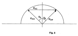
- the transducer launches an acoustic wave along an acoustic wave vector K AC , which is preferably normal to a transducer face.
- K DIF is the vector of the diffracted optical beam and K INC is the vector of the incident optical beam.
- the diffraction efficiency for the AO effect ⁇ is defined as the ratio between the intensity of the diffracted optical beam I 1 and the intensity of the incident optical beam I 0 .
- M 2 increases, the acoustic power P a required to reach a predetermined diffraction efficiency decreases. In turn, P a depends on the electrical power delivered to the transducer. Therefore as M 2 increases, less electrical power is required to reach the same diffraction efficiency.
- a good material is one in which a trade-off is found among the following requirements: elevated M2, low acoustic absorption coefficient, high thermal stability regarding acoustic and optical properties, chemical and mechanical stability, elevated optical transparency and low chromatic optical dispersion at the wavelength of interest (for example around 1.500 nm).
- low optical chromatic dispersion means that the magnitude of the dispersion be of the same order of magnitude of silica optical fibers (D ⁇ 17 ps/nm Km at 1550nm in SiO 2 fibers).
- TeO 2 tellurium oxide
- TeO 2 (tellurium oxide) based glass is the following composition: TeO 2 ( 62,5% wt.), WO 3 (32.36%wt.), MgO (0.55% wt.), Li 2 O ( 2.42% wt.), TiO 2 ( 2.17% wt.).
- TeO 2 is the main component and it contributes to high refractive index, low acoustic velocity, low acoustic absorption, optical transparency and low chromatic dispersion; WO 3 has been introduced in such a percentage, so as to contribute to an increase in the refractive index, without affecting other parameters; MgO is added in such a percentage in order to reduce the density of the glass, without increasing the acoustic velocity; Li 2 O and
- TiO 2 help the glass to vetrify; in addition TiO 2 increases the refractive index.
- the switching mechanism comprises said acousto-optic transducer which provides the commutation between a condition "on” and a condition “off” and vice versa.
- the above cited external control is preferably the radio frequency applied to said acousto-optic transducer.
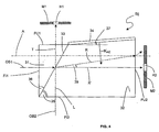
- FIG 4 an example of a generic switching element S ij is shown.
- said switching element comprises a first prism 31 and a second prism 32, the two prisms are bonded each other in a way to from a semi-transparent interface 33.
- the semi-transparent interface comprises at least a layer of an optical conductive medium, for example a thin layer of Au.
- the two prisms are bonded each other by means of glue.
- Said glue is preferably also an optical conductive medium.
- Said semi-transparent interface forms substantially a beam splitter in which an incident optical beam is partially transmitted and partially reflected.
- a splitter angle 35 is defined by the geometry of the two prisms and it represents the angle between the direction of said transparent interface and the side face of corresponding prism 32 input face FI2. Such angle determines the direction of the reflected beam of the semitransparent interface.
- said semi-transparent interface comprises at least a layer of conductive optical medium. More preferably, said semi-transparent interface comprises at least a layer of glue.
- said conductive optical medium and said glue are selected to form a dielectric multistrate substantially insensitive to the polarization of an optical beam.
- Said semi-transparent interface partially transmits and partially reflects an optical beam without distinguishing between polarizations status.
- the percentage of transmitted beam is chosen around 50%. But for special purposes the percentage of transmitted beam may be chosen with a different percentage; for example in a matrix, in which in said predetermined positions the commutations are more probable, it is advantageous to choose a lower percentage for the transmitted beam, for example 30%.
- a piezo-electric transducer plate 34 is provided on the top of the second prism 32 .
- said transducer When said transducer is fed with adequate electric current it generates acoustic waves which propagates into said second prism into the direction K AC which is preferably perpendicular to the plane of the transducer plate.
- Said plane of the transducer plate has preferably a plane angle 37, which is the angle between the direction of the plane of the transducer and parallel to input face FI2. Said plane angle is chosen in a way to form acoustic waves with a predetermined direction into the acoustic optic medium as detailed in the following
- said switching element comprises a first input face or port FI1 a second input face or port FI2 a first output face or port FU1 and a second output face or port FU2.
- said switching element comprises a first dark element M1, having a central hole H1 disposed in correspondence of said first output port and a second dark element M2, having a central hole H2, disposed in correspondence of said second output port.
- Said two dark elements transmit an optical beam directed into said holes and stop an optical beam directed in the other directions.
- Said dark elements are preferably metallic plates on which black layers are deposited.
- a first input beam OB1 entering from the first input port FI1 is transmitted to the second output port FU2.
- a second input beam OB2 entering from the second input port FI2 is partially reflected substantially to said second output port and partially transmitted to said first output port FU1.
- the reflected beam R is directed to the second output FU2 with an angulated direction with respect to the axis A.
- Said angle depends from the chosen splitting angle 35.
- said splitting angle is chosen in a way to direct said reflected beam R to said second dark element not in correspondence of the hole H2. In this way, the reflected optical beam is stopped from said second dark element M2.
- the acousto-optic diffraction medium is excited from the acoustic wave emitted from said piezoelectric plate.
- This wave causes a diffraction of the reflected optical beam and causes a change of the direction of propagation of the reflected optical beam.
- the diffraction optical beam angle changes in relationship with the frequency of said acoustic wave.
- Said frequency is chosen in a way to form a diffraction angle 39 which determines a diffracted optical beam R' preferably parallel to said axis A.
- the diffraction angle 39 is chosen in a way to direct the diffracted optical beam R' to the hole H2 of said dark element M2. In this way when the switching element is in "on” condition an optical beam from said second input port FI2 is directed to said second output port.
- the switching element S13 is activated into the "on”condition.
- Said switching element into the "on” condition transmits partially the optical beam to said first output port FU1 (see figure 4).
- Said potential crosstalk beam is stopped from the successive switch element S32 which is certainly in an off condition (to connect a input matrix port i to a output matrix port j only the Sij element is activated into the "on” condition).
- the matrix is designed in a way to stop the crosstalk of a partially transmitted optical beam of an "on” switch element, from another one switch element in the same row, which is certainly in the "off” condition.
- Each switching element in said activated condition has at least one further switching element inactive in the same matrix row and in a successive column. No crosstalk arises due to beams partially transmitted from a switching element in the last column, i.e. the column opposite to the inputs 21-23 in figure 2.
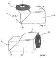
- FIG 6a and 6b an example of a switching element is shown.
- the two prisms are realized in TeO 2
- the partially-reflecting layer is made of a 6.45nm-thick Au layer, resulting in a 50% reflection of the s-polarized component and a 98 % reflection of the p-polarization component of the optical beam.
- the dependence on the polarization is a function of the incidence angle of the beams.
- the splitting angle 35 is around 45.5° and the plane angle 37 is around 0.5°.
- the frequency of the acoustic wave is chosen around 80 MHz.
- the transducer 34 is a thin plate of quartz (Si O 2 ).
- Said optical switching matrix as above described is designed preferably to use in an optical network with multiwavelength signals. For this reason the switching elements of the invention must be substantially insensitive at the wavelengths; in particular, the switching elements of the invention must be substantially insensitive at the wavelength preferably into the amplification band of optical amplifiers contained in such network.
- figure 7 a spectral response of the switching element of figure 6a and 6b is shown.
- the optical band is centered to a wavelength of 1550 nm, which is a typical wavelength value for a channel of a multi-wavelength signal of optical networks.
- the graph of figure 7 shows four curves, which are referred to different lengths of said transducer of figures 6a and 6b.
- Each curve is referred to a predetermined length of the transducer.
- the -3dB wavelength band (identified in figure 7 with the line B), which is a typical value of acceptable losses in a network band, is for example around 300 nm for a length of L of 10 millimeter. Said band is sufficient to cover an entire set of channels of a multi-wavelength signal in a dense multiwavelength system.
Landscapes
- Engineering & Computer Science (AREA)
- Computer Networks & Wireless Communication (AREA)
- Optical Modulation, Optical Deflection, Nonlinear Optics, Optical Demodulation, Optical Logic Elements (AREA)
- Mechanical Light Control Or Optical Switches (AREA)
Claims (12)
- Optische Schaltmatrix, umfassend:mindestens einen Eingangsmatrixport (21; 22; 23), der mindestens eine Zeile der Matrix definiert,eine Mehrzahl von Ausgangsmatrixports (24, 25, 26), die Spalten der Matrix definieren,eine Mehrzahl von Schaltelementen (S11, S12, S13, S21, S22, S23, S31, S32, S33), von denen jedes am Kreuzungspunkt der mindestens einen Zeile und einer der Spalten angeordnet ist,wobeijedes aus der Mehrzahl von Schaltelementen (S11, S12, S13, S21, S22, S23, S31, S32, S33) in einer vorgegebenen Position der Matrix, in einem aktivierten Zustand, einen Eingangsmatrixport (21; 22; 23) mit einem Ausgangsmatrixport (24; 25; 26) verbindet, wobei die Ports jeweils der vorgegebenen Position der Matrix entsprechen, undjedes aus der Mehrzahl von Schaltelementen (S11, S12, S13, S21, S22, S23, S31, S32, S33) einen akustooptischen Deflektor umfasst, um einen aus der Mehrzahl von Ausgangsmatrixports (24, 25, 26) auszuwählen,dadurch gekennzeichnet, dass der akustooptische Deflektor ein akustooptisches Medium umfasst, welches eine halbtransparente Grenzfläche (33) umfasst, die ausgebildet ist, um einen optischen Strahl teilweise zu reflektieren und teilweise zu transmittieren.
- Optische Schaltmatrix nach Anspruch 1, wobei für jedes Schaltelement (S11; S12; S13; S21; S22; S23; S31; S32; S33) in dem aktivierten Zustand die Matrix mindestens ein weiteres Schaltelement (S11; S12; S13; S21; S22; S23; S31; S32; S33) umfasst, welches in derselben Matrixzeile und einer nachfolgenden Spalte inaktiv ist.
- Optische Schaltmatrix nach Anspruch 1 oder 2, weiterhin umfassend ein Substrat (2), auf welchem die Schaltelemente (S11, S12, S13, S21, S22, S23, S31, S32, S33) vorgesehen sind, und eine Mehrzahl von Wellenleitern, in welchen optische Signale von dem mindestens einen Eingangsmatrixport (21; 22; 23) zu den Schaltelementen (S11, S12, S13, S21, S22, S23, S31, S32, S33) und von den Schaltelementen (S11, S12, S13, S21, S22, S23, S31, S32, S33) zu der Mehrzahl von Ausgangsmatrixports (24, 25, 26) geleitet werden.
- Optische Schaltmatrix nach einem beliebigen der Ansprüche 1 bis 3, wobei jedes aus der Mehrzahl von Schaltelementen (S11, S12, S13, S21, S22, S23, S31, S32, S33) weiterhin umfasst:mindestens einen Eingangsport (FI1; FI2),eine Mehrzahl von Ausgangsports (FU1, FU2),einen Schaltmechanismus, welcher das Schaltelement durch Erzeugen akustischer Wellen in dem akustooptischen Medium aktiviert,wobei der transmittierte optische Strahl durch die halbtransparente Oberfläche (33) von dem mindestens einen Eingangsport (FI1; FI2) zu einem aus der Mehrzahl von Ausgangsports (FU1, FU2) gesendet wird, und der reflektierte optische Strahl durch die halbtransparente Oberfläche (33) von dem akustooptischen Medium gebeugt wird, wenn es durch den Schaltmechanismus aktiviert wird, von dem mindestens einen Eingangsport (FI1; FI2) zu einem anderen Port aus der Mehrzahl von Ausgangsports (FU1, FU2).
- Optische Schaltmatrix nach einem beliebigen der Ansprüche 1 bis 4, weiterhin umfassend ein erstes Prisma (31) und ein zweites Prisma (32), welche in dem akustooptischen Medium realisiert sind und miteinander auf eine Weise verbunden sind, so dass sie die halbtransparente Grenzfläche (33) bilden.
- Optische Schaltmatrix nach einem beliebigen der Ansprüche 1 bis 5, wobei die halbtransparente Grenzfläche (33) mindestens ein optisch leitfähiges Medium umfasst.
- Optische Schaltmatrix nach einem beliebigen der Ansprüche 1 bis 6, wobei das akustooptische Medium ein isotropisches akustooptisches Diffraktionsmedium ist.
- Optische Schaltmatrix nach Anspruch 4, wobei der Schaltmechanismus einen piezoelektrischen Wandler (34) umfasst.
- Optische Schaltmatrix nach Anspruch 8, wobei der piezoelektrische Wandler (34) eine piezoelektrische Wandlerplatte umfasst.
- Optische Schaltmatrix nach Anspruch 9 und 5, wobei die piezoelektrische Wandlerplatte an dem oberen Ende des zweiten Prismas (32) verbunden ist.
- Optische Schaltmatrix nach Anspruch 4, weiterhin umfassend dunkle Elemente, die mittige Löcher aufweisen, welche in Übereinstimmung mit jeweils einem aus der Mehrzahl von Ausgangsports (FU1, FU2) angeordnet sind.
- Optische Schaltmatrix nach einem beliebigen der Ansprüche 1 bis 11, wobei die halbtransparente Oberfläche (33) gegenüber der Polarisation des optischen Strahles im Wesentlichen unempfindlich ist.
Priority Applications (1)
| Application Number | Priority Date | Filing Date | Title |
|---|---|---|---|
| AT01995682T ATE318059T1 (de) | 2001-11-30 | 2001-11-30 | Optische raumschaltmatrix |
Applications Claiming Priority (1)
| Application Number | Priority Date | Filing Date | Title |
|---|---|---|---|
| PCT/EP2001/013996 WO2003047304A1 (en) | 2001-11-30 | 2001-11-30 | Optical space-switching matrix |
Publications (2)
| Publication Number | Publication Date |
|---|---|
| EP1449403A1 EP1449403A1 (de) | 2004-08-25 |
| EP1449403B1 true EP1449403B1 (de) | 2006-02-15 |
Family
ID=8164704
Family Applications (1)
| Application Number | Title | Priority Date | Filing Date |
|---|---|---|---|
| EP01995682A Expired - Lifetime EP1449403B1 (de) | 2001-11-30 | 2001-11-30 | Optische raumschaltmatrix |
Country Status (6)
| Country | Link |
|---|---|
| US (1) | US7209607B2 (de) |
| EP (1) | EP1449403B1 (de) |
| AU (1) | AU2002226367A1 (de) |
| CA (1) | CA2467668C (de) |
| DE (1) | DE60117292T2 (de) |
| WO (1) | WO2003047304A1 (de) |
Families Citing this family (5)
| Publication number | Priority date | Publication date | Assignee | Title |
|---|---|---|---|---|
| US8687267B2 (en) * | 2009-02-24 | 2014-04-01 | Peiliang GAO | Optical wavelength tunable filter |
| WO2012172760A1 (ja) * | 2011-06-14 | 2012-12-20 | 日本電気株式会社 | 光スイッチ制御方法、光スイッチ制御装置、および光伝送システム |
| CN104216052A (zh) * | 2013-05-29 | 2014-12-17 | 鸿富锦精密工业(深圳)有限公司 | 光信号传输装置 |
| TWI572926B (zh) * | 2013-05-29 | 2017-03-01 | 鴻海精密工業股份有限公司 | 光訊號傳輸裝置 |
| CN107765370B (zh) * | 2016-08-17 | 2020-01-03 | 华为技术有限公司 | 光交叉连接装置 |
Family Cites Families (11)
| Publication number | Priority date | Publication date | Assignee | Title |
|---|---|---|---|---|
| US3602577A (en) * | 1970-03-17 | 1971-08-31 | George W Byram | Optical tunneling acoustic surface wave light modulator |
| US3871743A (en) * | 1973-06-04 | 1975-03-18 | Gte Laboratories Inc | Optical crosspoint switching matrix for an optical communications system |
| JPS6010229A (ja) * | 1983-06-30 | 1985-01-19 | Hoya Corp | 音響光学偏向装置 |
| US4995693A (en) * | 1988-08-05 | 1991-02-26 | Unisys Corporation | Multi-position opto-electronic switch |
| JP2928046B2 (ja) * | 1993-04-16 | 1999-07-28 | 日本電気株式会社 | 光ネットワ−ク及びその障害回復方式 |
| US5909304A (en) * | 1994-04-19 | 1999-06-01 | Aurora Photonics, Inc. | Acousto-optic tunable filter based on isotropic acousto-optic diffraction using phased array transducers |
| US5703710A (en) * | 1994-09-09 | 1997-12-30 | Deacon Research | Method for manipulating optical energy using poled structure |
| US5581643A (en) * | 1994-12-08 | 1996-12-03 | Northern Telecom Limited | Optical waveguide cross-point switch |
| US6016216A (en) * | 1997-05-17 | 2000-01-18 | Aurora Photonics, Inc. | Polarization-independent acousto-optic tunable filter |
| US6049641A (en) * | 1998-02-24 | 2000-04-11 | Gemfire Corporation | Connection system for optical redundancy |
| WO2000076252A1 (en) | 1999-06-04 | 2000-12-14 | Chorum Technologies Lp | Optical add/drop wavelength switch using a high extinction ratio polarization beamsplitter |
-
2001
- 2001-11-30 AU AU2002226367A patent/AU2002226367A1/en not_active Abandoned
- 2001-11-30 US US10/497,009 patent/US7209607B2/en not_active Expired - Fee Related
- 2001-11-30 WO PCT/EP2001/013996 patent/WO2003047304A1/en not_active Ceased
- 2001-11-30 EP EP01995682A patent/EP1449403B1/de not_active Expired - Lifetime
- 2001-11-30 CA CA2467668A patent/CA2467668C/en not_active Expired - Fee Related
- 2001-11-30 DE DE60117292T patent/DE60117292T2/de not_active Expired - Lifetime
Also Published As
| Publication number | Publication date |
|---|---|
| DE60117292D1 (de) | 2006-04-20 |
| EP1449403A1 (de) | 2004-08-25 |
| AU2002226367A1 (en) | 2003-06-10 |
| WO2003047304A1 (en) | 2003-06-05 |
| US20050041911A1 (en) | 2005-02-24 |
| US7209607B2 (en) | 2007-04-24 |
| CA2467668C (en) | 2010-07-13 |
| DE60117292T2 (de) | 2006-11-02 |
| CA2467668A1 (en) | 2003-06-05 |
Similar Documents
| Publication | Publication Date | Title |
|---|---|---|
| Riza et al. | Reconfigurable wavelength add-drop filtering based on a Banyan network topology and ferroelectric liquid crystal fiber-optic switches | |
| EP1332391B1 (de) | Planarer wellenleiterschalter und optischer crossconnect | |
| EP0701710B1 (de) | Frequenzselektiver optischer schalter mit der verwendung von polarisationsdrehung | |
| Patel et al. | Liquid crystal and grating-based multiple-wavelength cross-connect switch | |
| US8731403B2 (en) | Multicast optical switch | |
| AU2004290090B2 (en) | Wavelength manipulation system and method | |
| JPH10507281A (ja) | 極化構造を用いて光学エネルギーを操作する方法 | |
| JPH10507846A (ja) | 電気的に制御できる格子反射鏡を備えたレーザ | |
| US7092594B2 (en) | Wavelength selector switch | |
| US6865310B2 (en) | Multi-layer thin film optical waveguide switch | |
| EP1202091B1 (de) | Ein polarisationsunabhängiger, konfigurierbarer, optischer Multiplexer | |
| JPH09166795A (ja) | 波長選択型の音響−光学導波路装置 | |
| US7209607B2 (en) | Optical space-switching matrix | |
| US9521474B2 (en) | Wavelength selective switch having multi-layer reflector | |
| JPWO2004102254A1 (ja) | 光デバイス | |
| US6819818B2 (en) | Optical switches having a common waveguide for improved switch performance | |
| US6778726B2 (en) | Optical switch | |
| US20090274409A1 (en) | Selectively Enhancing Angular Beam Deflection | |
| US20050013523A1 (en) | Optical add drop multiplexer device | |
| Yuan et al. | Optical switches | |
| US6847755B2 (en) | Optical cross connection switch using voltage-controlled interferometric optical switching elements | |
| Herrmann | Acousto-Optical Devices | |
| Smit et al. | Wavelength-selective devices | |
| KR20010089707A (ko) | 음향-광학 장치 | |
| JP2004020718A (ja) | 光スイッチモジュール |
Legal Events
| Date | Code | Title | Description |
|---|---|---|---|
| PUAI | Public reference made under article 153(3) epc to a published international application that has entered the european phase |
Free format text: ORIGINAL CODE: 0009012 |
|
| 17P | Request for examination filed |
Effective date: 20040511 |
|
| AK | Designated contracting states |
Kind code of ref document: A1 Designated state(s): AT BE CH CY DE DK ES FI FR GB GR IE IT LI LU MC NL PT SE TR |
|
| AX | Request for extension of the european patent |
Extension state: AL LT LV MK RO SI |
|
| 17Q | First examination report despatched |
Effective date: 20040908 |
|
| RIN1 | Information on inventor provided before grant (corrected) |
Inventor name: ZAPPETTINI, ANDREA Inventor name: PIETRALUNGA, SILVIA, MARIA Inventor name: MARTINELLI, MARIO Inventor name: PAGANINI, ANDREA |
|
| GRAP | Despatch of communication of intention to grant a patent |
Free format text: ORIGINAL CODE: EPIDOSNIGR1 |
|
| GRAS | Grant fee paid |
Free format text: ORIGINAL CODE: EPIDOSNIGR3 |
|
| GRAA | (expected) grant |
Free format text: ORIGINAL CODE: 0009210 |
|
| AK | Designated contracting states |
Kind code of ref document: B1 Designated state(s): AT BE CH CY DE DK ES FI FR GB GR IE IT LI LU MC NL PT SE TR |
|
| PG25 | Lapsed in a contracting state [announced via postgrant information from national office to epo] |
Ref country code: IT Free format text: LAPSE BECAUSE OF FAILURE TO SUBMIT A TRANSLATION OF THE DESCRIPTION OR TO PAY THE FEE WITHIN THE PRESCRIBED TIME-LIMIT;WARNING: LAPSES OF ITALIAN PATENTS WITH EFFECTIVE DATE BEFORE 2007 MAY HAVE OCCURRED AT ANY TIME BEFORE 2007. THE CORRECT EFFECTIVE DATE MAY BE DIFFERENT FROM THE ONE RECORDED. Effective date: 20060215 Ref country code: CH Free format text: LAPSE BECAUSE OF FAILURE TO SUBMIT A TRANSLATION OF THE DESCRIPTION OR TO PAY THE FEE WITHIN THE PRESCRIBED TIME-LIMIT Effective date: 20060215 Ref country code: BE Free format text: LAPSE BECAUSE OF FAILURE TO SUBMIT A TRANSLATION OF THE DESCRIPTION OR TO PAY THE FEE WITHIN THE PRESCRIBED TIME-LIMIT Effective date: 20060215 Ref country code: LI Free format text: LAPSE BECAUSE OF FAILURE TO SUBMIT A TRANSLATION OF THE DESCRIPTION OR TO PAY THE FEE WITHIN THE PRESCRIBED TIME-LIMIT Effective date: 20060215 Ref country code: AT Free format text: LAPSE BECAUSE OF FAILURE TO SUBMIT A TRANSLATION OF THE DESCRIPTION OR TO PAY THE FEE WITHIN THE PRESCRIBED TIME-LIMIT Effective date: 20060215 Ref country code: FI Free format text: LAPSE BECAUSE OF FAILURE TO SUBMIT A TRANSLATION OF THE DESCRIPTION OR TO PAY THE FEE WITHIN THE PRESCRIBED TIME-LIMIT Effective date: 20060215 Ref country code: NL Free format text: LAPSE BECAUSE OF FAILURE TO SUBMIT A TRANSLATION OF THE DESCRIPTION OR TO PAY THE FEE WITHIN THE PRESCRIBED TIME-LIMIT Effective date: 20060215 |
|
| REG | Reference to a national code |
Ref country code: CH Ref legal event code: EP Ref country code: GB Ref legal event code: FG4D |
|
| REG | Reference to a national code |
Ref country code: IE Ref legal event code: FG4D |
|
| REF | Corresponds to: |
Ref document number: 60117292 Country of ref document: DE Date of ref document: 20060420 Kind code of ref document: P |
|
| REG | Reference to a national code |
Ref country code: DE Ref legal event code: R096 Ref document number: 60117292 Country of ref document: DE Effective date: 20060420 |
|
| PG25 | Lapsed in a contracting state [announced via postgrant information from national office to epo] |
Ref country code: DK Free format text: LAPSE BECAUSE OF FAILURE TO SUBMIT A TRANSLATION OF THE DESCRIPTION OR TO PAY THE FEE WITHIN THE PRESCRIBED TIME-LIMIT Effective date: 20060515 Ref country code: SE Free format text: LAPSE BECAUSE OF FAILURE TO SUBMIT A TRANSLATION OF THE DESCRIPTION OR TO PAY THE FEE WITHIN THE PRESCRIBED TIME-LIMIT Effective date: 20060515 |
|
| PG25 | Lapsed in a contracting state [announced via postgrant information from national office to epo] |
Ref country code: ES Free format text: LAPSE BECAUSE OF FAILURE TO SUBMIT A TRANSLATION OF THE DESCRIPTION OR TO PAY THE FEE WITHIN THE PRESCRIBED TIME-LIMIT Effective date: 20060526 |
|
| PG25 | Lapsed in a contracting state [announced via postgrant information from national office to epo] |
Ref country code: PT Free format text: LAPSE BECAUSE OF FAILURE TO SUBMIT A TRANSLATION OF THE DESCRIPTION OR TO PAY THE FEE WITHIN THE PRESCRIBED TIME-LIMIT Effective date: 20060717 |
|
| NLV1 | Nl: lapsed or annulled due to failure to fulfill the requirements of art. 29p and 29m of the patents act | ||
| REG | Reference to a national code |
Ref country code: CH Ref legal event code: PL |
|
| ET | Fr: translation filed | ||
| PG25 | Lapsed in a contracting state [announced via postgrant information from national office to epo] |
Ref country code: IE Free format text: LAPSE BECAUSE OF NON-PAYMENT OF DUE FEES Effective date: 20061130 Ref country code: MC Free format text: LAPSE BECAUSE OF NON-PAYMENT OF DUE FEES Effective date: 20061130 |
|
| PLBE | No opposition filed within time limit |
Free format text: ORIGINAL CODE: 0009261 |
|
| STAA | Information on the status of an ep patent application or granted ep patent |
Free format text: STATUS: NO OPPOSITION FILED WITHIN TIME LIMIT |
|
| 26N | No opposition filed |
Effective date: 20061116 |
|
| REG | Reference to a national code |
Ref country code: DE Ref legal event code: R097 Ref document number: 60117292 Country of ref document: DE Effective date: 20061116 |
|
| PG25 | Lapsed in a contracting state [announced via postgrant information from national office to epo] |
Ref country code: GR Free format text: LAPSE BECAUSE OF FAILURE TO SUBMIT A TRANSLATION OF THE DESCRIPTION OR TO PAY THE FEE WITHIN THE PRESCRIBED TIME-LIMIT Effective date: 20060516 |
|
| PG25 | Lapsed in a contracting state [announced via postgrant information from national office to epo] |
Ref country code: LU Free format text: LAPSE BECAUSE OF NON-PAYMENT OF DUE FEES Effective date: 20061130 Ref country code: TR Free format text: LAPSE BECAUSE OF FAILURE TO SUBMIT A TRANSLATION OF THE DESCRIPTION OR TO PAY THE FEE WITHIN THE PRESCRIBED TIME-LIMIT Effective date: 20060215 |
|
| PG25 | Lapsed in a contracting state [announced via postgrant information from national office to epo] |
Ref country code: CY Free format text: LAPSE BECAUSE OF FAILURE TO SUBMIT A TRANSLATION OF THE DESCRIPTION OR TO PAY THE FEE WITHIN THE PRESCRIBED TIME-LIMIT Effective date: 20060215 |
|
| PGFP | Annual fee paid to national office [announced via postgrant information from national office to epo] |
Ref country code: IT Payment date: 20101111 Year of fee payment: 10 |
|
| REG | Reference to a national code |
Ref country code: DE Ref legal event code: R082 Ref document number: 60117292 Country of ref document: DE Representative=s name: MANITZ, FINSTERWALD & PARTNER GBR, DE Effective date: 20120209 Ref country code: DE Ref legal event code: R081 Ref document number: 60117292 Country of ref document: DE Owner name: GOOGLE, INC., US Free format text: FORMER OWNER: PIRELLI & C. S.P.A., MAILAND/MILANO, IT Effective date: 20120209 Ref country code: DE Ref legal event code: R081 Ref document number: 60117292 Country of ref document: DE Owner name: GOOGLE, INC., MOUNTAIN VIEW, US Free format text: FORMER OWNER: PIRELLI & C. S.P.A., MAILAND/MILANO, IT Effective date: 20120209 Ref country code: DE Ref legal event code: R082 Ref document number: 60117292 Country of ref document: DE Representative=s name: MANITZ FINSTERWALD PATENT- UND RECHTSANWALTSPA, DE Effective date: 20120209 Ref country code: DE Ref legal event code: R082 Ref document number: 60117292 Country of ref document: DE Representative=s name: MANITZ FINSTERWALD PATENTANWAELTE PARTMBB, DE Effective date: 20120209 Ref country code: DE Ref legal event code: R081 Ref document number: 60117292 Country of ref document: DE Owner name: GOOGLE LLC (N.D.GES.D. STAATES DELAWARE), MOUN, US Free format text: FORMER OWNER: PIRELLI & C. S.P.A., MAILAND/MILANO, IT Effective date: 20120209 |
|
| REG | Reference to a national code |
Ref country code: FR Ref legal event code: TP Owner name: MOSAID TECHNOLOGIES INCORPORATED, CA Effective date: 20120320 |
|
| REG | Reference to a national code |
Ref country code: GB Ref legal event code: 732E Free format text: REGISTERED BETWEEN 20120329 AND 20120404 |
|
| REG | Reference to a national code |
Ref country code: DE Ref legal event code: R082 Ref document number: 60117292 Country of ref document: DE Representative=s name: MANITZ, FINSTERWALD & PARTNER GBR, DE |
|
| REG | Reference to a national code |
Ref country code: GB Ref legal event code: 732E Free format text: REGISTERED BETWEEN 20120628 AND 20120704 |
|
| REG | Reference to a national code |
Ref country code: DE Ref legal event code: R082 Ref document number: 60117292 Country of ref document: DE Representative=s name: MANITZ, FINSTERWALD & PARTNER GBR, DE Effective date: 20120710 Ref country code: DE Ref legal event code: R081 Ref document number: 60117292 Country of ref document: DE Owner name: GOOGLE, INC., MOUNTAIN VIEW, US Free format text: FORMER OWNER: MOSAID TECHNOLOGIES INCORPORATED, OTTAWA, ONTARIO, CA Effective date: 20120710 Ref country code: DE Ref legal event code: R082 Ref document number: 60117292 Country of ref document: DE Representative=s name: MANITZ FINSTERWALD PATENT- UND RECHTSANWALTSPA, DE Effective date: 20120710 Ref country code: DE Ref legal event code: R082 Ref document number: 60117292 Country of ref document: DE Representative=s name: MANITZ FINSTERWALD PATENTANWAELTE PARTMBB, DE Effective date: 20120710 Ref country code: DE Ref legal event code: R081 Ref document number: 60117292 Country of ref document: DE Owner name: GOOGLE LLC (N.D.GES.D. STAATES DELAWARE), MOUN, US Free format text: FORMER OWNER: MOSAID TECHNOLOGIES INCORPORATED, OTTAWA, ONTARIO, CA Effective date: 20120710 |
|
| REG | Reference to a national code |
Ref country code: FR Ref legal event code: TP Owner name: GOOGLE INC., US Effective date: 20120730 |
|
| PG25 | Lapsed in a contracting state [announced via postgrant information from national office to epo] |
Ref country code: IT Free format text: LAPSE BECAUSE OF NON-PAYMENT OF DUE FEES Effective date: 20121130 |
|
| REG | Reference to a national code |
Ref country code: FR Ref legal event code: PLFP Year of fee payment: 15 |
|
| REG | Reference to a national code |
Ref country code: FR Ref legal event code: PLFP Year of fee payment: 16 |
|
| REG | Reference to a national code |
Ref country code: FR Ref legal event code: PLFP Year of fee payment: 17 |
|
| PGFP | Annual fee paid to national office [announced via postgrant information from national office to epo] |
Ref country code: DE Payment date: 20171129 Year of fee payment: 17 Ref country code: FR Payment date: 20171127 Year of fee payment: 17 |
|
| REG | Reference to a national code |
Ref country code: DE Ref legal event code: R082 Ref document number: 60117292 Country of ref document: DE Representative=s name: MANITZ FINSTERWALD PATENT- UND RECHTSANWALTSPA, DE Ref country code: DE Ref legal event code: R082 Ref document number: 60117292 Country of ref document: DE Representative=s name: MANITZ FINSTERWALD PATENTANWAELTE PARTMBB, DE Ref country code: DE Ref legal event code: R081 Ref document number: 60117292 Country of ref document: DE Owner name: GOOGLE LLC (N.D.GES.D. STAATES DELAWARE), MOUN, US Free format text: FORMER OWNER: GOOGLE, INC., MOUNTAIN VIEW, CALIF., US |
|
| PGFP | Annual fee paid to national office [announced via postgrant information from national office to epo] |
Ref country code: GB Payment date: 20171127 Year of fee payment: 17 |
|
| REG | Reference to a national code |
Ref country code: FR Ref legal event code: CD Owner name: GOOGLE INC., US Effective date: 20180213 Ref country code: FR Ref legal event code: CJ Effective date: 20180213 |
|
| REG | Reference to a national code |
Ref country code: DE Ref legal event code: R119 Ref document number: 60117292 Country of ref document: DE |
|
| GBPC | Gb: european patent ceased through non-payment of renewal fee |
Effective date: 20181130 |
|
| PG25 | Lapsed in a contracting state [announced via postgrant information from national office to epo] |
Ref country code: DE Free format text: LAPSE BECAUSE OF NON-PAYMENT OF DUE FEES Effective date: 20190601 Ref country code: FR Free format text: LAPSE BECAUSE OF NON-PAYMENT OF DUE FEES Effective date: 20181130 |
|
| PG25 | Lapsed in a contracting state [announced via postgrant information from national office to epo] |
Ref country code: GB Free format text: LAPSE BECAUSE OF NON-PAYMENT OF DUE FEES Effective date: 20181130 |
|
| P01 | Opt-out of the competence of the unified patent court (upc) registered |
Effective date: 20230516 |