EP1447813A1 - Memory built-in self repair (MBISR) circuits / devices and method for repairing a memory comprising a memory built-in self repair (MBISR) structure - Google Patents
Memory built-in self repair (MBISR) circuits / devices and method for repairing a memory comprising a memory built-in self repair (MBISR) structure Download PDFInfo
- Publication number
- EP1447813A1 EP1447813A1 EP03002698A EP03002698A EP1447813A1 EP 1447813 A1 EP1447813 A1 EP 1447813A1 EP 03002698 A EP03002698 A EP 03002698A EP 03002698 A EP03002698 A EP 03002698A EP 1447813 A1 EP1447813 A1 EP 1447813A1
- Authority
- EP
- European Patent Office
- Prior art keywords
- row
- column
- register
- mbisr
- memory built
- Prior art date
- Legal status (The legal status is an assumption and is not a legal conclusion. Google has not performed a legal analysis and makes no representation as to the accuracy of the status listed.)
- Granted
Links
- 230000015654 memory Effects 0.000 title claims abstract description 261
- 238000000034 method Methods 0.000 title claims abstract description 36
- 230000002950 deficient Effects 0.000 claims abstract description 19
- 210000000352 storage cell Anatomy 0.000 claims abstract description 13
- 238000001514 detection method Methods 0.000 claims abstract description 12
- 238000013459 approach Methods 0.000 claims abstract description 9
- 239000000872 buffer Substances 0.000 claims description 66
- 238000012360 testing method Methods 0.000 claims description 59
- 210000004027 cell Anatomy 0.000 claims description 56
- 230000004913 activation Effects 0.000 claims description 22
- 230000003213 activating effect Effects 0.000 claims description 8
- 230000003068 static effect Effects 0.000 claims description 4
- 230000007547 defect Effects 0.000 description 15
- 238000003491 array Methods 0.000 description 5
- 238000004364 calculation method Methods 0.000 description 5
- 238000012545 processing Methods 0.000 description 5
- 238000010586 diagram Methods 0.000 description 2
- 238000004519 manufacturing process Methods 0.000 description 2
- 238000013461 design Methods 0.000 description 1
- 238000005516 engineering process Methods 0.000 description 1
- 230000003116 impacting effect Effects 0.000 description 1
- 230000008520 organization Effects 0.000 description 1
- 239000002699 waste material Substances 0.000 description 1
Images




Classifications
-
- G—PHYSICS
- G11—INFORMATION STORAGE
- G11C—STATIC STORES
- G11C29/00—Checking stores for correct operation ; Subsequent repair; Testing stores during standby or offline operation
- G11C29/70—Masking faults in memories by using spares or by reconfiguring
- G11C29/72—Masking faults in memories by using spares or by reconfiguring with optimized replacement algorithms
-
- G—PHYSICS
- G11—INFORMATION STORAGE
- G11C—STATIC STORES
- G11C29/00—Checking stores for correct operation ; Subsequent repair; Testing stores during standby or offline operation
- G11C29/70—Masking faults in memories by using spares or by reconfiguring
- G11C29/78—Masking faults in memories by using spares or by reconfiguring using programmable devices
- G11C29/80—Masking faults in memories by using spares or by reconfiguring using programmable devices with improved layout
- G11C29/81—Masking faults in memories by using spares or by reconfiguring using programmable devices with improved layout using a hierarchical redundancy scheme
Definitions
- the invention relates to a method for repairing a memory comprising a Memory Built-In Self Repair (MBISR) structure according to the pre-characterizing portion of claim 1, to a Memory Built-In Self Repair (MBISR) device according to the pre-characterizing portion of claim 9, to a Memory Built-In Self Repair (MBISR) device according to the pre-characterizing portion of claim 28, to a Column Memory Built-In Self Repair (MBISR) circuit, and to a Row Memory Built-In Self Repair (MBISR) circuit.
- MBISR Memory Built-In Self Repair
- Digital memories consist of two-dimensional arrays of elements (storage cells) each capable of storing N different data values, where N is the number of stable states of the storage cell; cells are arranged into rows and columns.
- memories may contain randomly distributed defective cells after fabrication which cause the memory to be unusable even if faults affect very small parts of the entire cell array.
- groups of spare storage cells are provided which allow replacing the defective ones once they are detected.
- MBISR Memory Built-In Self Repair
- New repair strategies are able to repair small groups of logically neighbouring cells (memory words) instead of complete rows and columns; word replacement is more flexible than row and column replacement in that it allows fixing sparse faulty cells, but it's not suitable for repairing column or periphery defects and, to some extent, row defects. Repair algorithms are not necessary for this type of redundancy as words are replaced at testing run time after detection of faults.
- the data of all defective cells need to be stored for processing; in general, complex processing is required to identify the optimal repair configuration.
- the corresponding calculations are done either on or off chip.
- Optimal repair configurations may not be identified due to unefficient processing, thus leading to discard memories which might be repaired instead.
- MBISR Memory Built-In Self Repair
- MBISR Memory Built-In Self Repair
- this object is achieved by a method according to claim 1, by a Memory Built-In Self Repair (MBISR) device according to claim 9, by a Memory Built-In Self Repair (MBISR) device according to claim 28, by a Column Memory Built-In Self Repair (MBISR) circuit according to claim 47, and by a Row Memory Built-In Self Repair (MBISR) circuit according to claim 50.
- MBISR Memory Built-In Self Repair
- MISR Memory Built-In Self Repair
- Preferred and advantageous developements of the method according to the invention are subject matter of claims 2 to 8.
- Preferred and advantageous embodiments of the Memory Built-In Self Repair (MBISR) device according to claim 9 are subject matter of claims 10 to 27.
- Preferred and advantageous embodiments of the Memory Built-In Self Repair (MBISR) device according to claim 28 are subject matter of claims 29 to 46.
- Preferred and advantageous embodiments of the Column Memory Built-In Self Repair (MBISR) circuit according to claim 47 are subject matter of claims 48 and 49.
- Preferred and advantageous embodiments of the Row Memory Built-In Self Repair (MBISR) circuit according to claim 50 are subject matter of claims 51 and 52.
- the idea realized by the method according to the invention and by the Memory Built-In Self Repair (MBISR) device according to claim 28 consists of a Memory Built-In Self Repair (MBISR) structure and a redundancy allocation method with related circuit infrastructure, combining classical repair strategies (row and column replacement) with new approaches (word replacement) to optimize the allocation of available redundant resources and to achieve the highest possible repair rate for any given memory configuration.
- MBISR Memory Built-In Self Repair
- MBISR Memory Built-In Self Repair
- MBISR Memory Built-In Self Repair
- MBIST Memory Built-In Self Test
- the device structure according to claim 9 as well as the circuit structures according to claims 47 and 50 allow fast calculation of spare row/column allocation without impacting the duration of MBIST (Memory Built-In Self Test) tests.
- MBIST Memory Built-In Self Test
- Memory arrays with MBISRs may be grouped to form larger memory subsystems; either single or grouped arrays are provided with a set of shared spare words which are used to repair faulty cells not covered by row and column redundancies.
- the circuits When used in combination with word redundancies, the circuits allow minimizing the number of spare rows and columns thus leading to significantly reducing the system area, power and cost.
- One single MBIST may serve multiple memories with row/column and word redundancies.
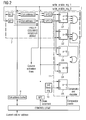
- Figs. 1 and 2 are more detailed representation of a Column Memory Built-In Self Repair (MBISR) circuit 3, which Column Memory Built-In Self Repair (MBISR) circuit 3 is part of the scheme of Fig. 1.
- MBISR Memory Built-In Self Repair
- Each memory array 2 (cf. also Fig. 3) with a given amount of spare rows and columns is provided with two independent spare row/column allocation circuits (Memory Built-In Self Repair (MBISR),circuits) 3, i.e. one Column Memory Built-In Self Repair (MBISR) circuit (cf. Fig. 2), and one Row Memory Built-In Self Repair (MBISR) circuit.
- MBISR Memory Built-In Self Repair
- Each of the row/column allocation circuits 3 contains a set of faulty row/column registers which point to the rows and columns to be replaced, a comparator/decoder 11 which selects the faulty row/column registers to compare or write to during the memory tests, and a control logic which synchronizes the operation with the different test phases (row or column test) and provides the interface to non volatile faulty row/column storage elements (fuses).
- Fig. 3 shows an overall diagram of a memory unit 5 made of multiple memories with row/column redundancies 2, each provided with a dedicated MBISR 3, and a shared word redundancy block 4.
- the memory unit 5 is connected to a standard Memory Built-In Self Test controller (MBIST) 8 and a bank of non volatile storage elements (fuses) 12 serving all MBISRs 3 and the word redundancy block 4.
- MBIST Memory Built-In Self Test controller
- fuses non volatile storage elements
- each MBISR 3 as shown in Fig. 3 consists of one Column Memory Built-In Self Repair (MBISR) circuit and one Row Memory Built-In Self Repair (MBISR) circuit as to be seen in Fig. 1.
- MBISR Column Memory Built-In Self Repair
- MBISR Row Memory Built-In Self Repair
- a Memory Built-In Self Repair (MBISR) device as shown in Fig. 3 is an embodiment of the Memory Built-In Self Repair (MBISR) device according to claim 9 and concurrently an embodiment of the Memory Built-In Self Repair (MBISR) device according to claim 28.
- Alternate configurations of embodiments of the Memory Built-In Self Repair (MBISR) device according to claim 28 alone may contain only one set of row/column allocation circuits shared by all memory arrays 2 with spare rows and columns.
- the spare row/column allocation method according to the present example is based on the simple rule that spare rows and columns must replace array rows and columns with the highest number of faulty cells; faulty cells not covered by row/column redundancy, if any, will be replaced by redundant words as long as they are available, otherwise a FAIL signal is activated to flag that the memory 2 is not repairable.
- the tester must check an entire row or column at a time and not portions of them.
- Row and column tests can be executed in any order, depending on which detection and repair strategy best fits the most frequent defects for any given memory technology.
- a column address buffer 9 (cf. Fig. 1) stores the address of the last column accessed; a Number of Faults in Column register (NFC) (cf. Fig. 1) is incremented each time a fault in the column pointed by the Col address buffer 9 is detected, thus storing the number of faulty cells belonging to that column.
- NFC Number of Faults in Column register
- the value stored in the NFC register is compared with a fixed first threshold beyond which it is considered worth to replace an entire column in the cell array; if there are too few faulty cells in a column, that may be even fixed by using redundant words or wordlines instead, the NFC register is cleared and calculation restarts from the next column being tested (if the first threshold value is set to 0, a spare column might be used to fix an array column with at least 1 defective cell).
- the value of the column replacement threshold i.e. the first threshold, is stored in a column threshold register 13 (see figure 1).
- the current value in the NFC register is compared to those stored in NFC(i) registers of a faulty columns register array 7, where the index i ranges from 1 to the number n of available spare columns (see Fig. 1).
- a Row address buffer 10 points to the last row accessed; a Number of Faults in Row (NFR) register (cf. Fig. 1) is incremented each time a fault in the row pointed by the Row address buffer 10 is detected, thus storing the number of faulty cells belonging to that row.
- NFR Number of Faults in Row
- the value stored in the NFR register is compared with a fixed second threshold beyond which it is considered worth to replace an entire row in the cell array; if there are too few faulty cells in a row, that may be even fixed by using redundant words instead, the NFR register is cleared and calculation restarts from the next row being tested (if the second threshold value is set to 0, a spare row might be used to fix an array row with at least 1 defective cell).
- the value of the row replacement threshold i.e. the second threshold, is stored in a row threshold register 14 (see Fig. 1).
- the current value in the NFR register is compared to those stored in the NFR(k) registers of a faulty rows register array 15, where the index k ranges from l to the number m of available spare rows (cf. Fig. 1).
- the values in the Row address buffer 10 and NFR registers are copied to the Row address register (l) and NFR (l) pair with the lowest value NFR (l) among all current NFR (k); an Activation Flag AF (l) being (re)asserted to indicate that the Row address register (l) register contains an effective faulty row address.
- the main advantage of this method consists of handling only the number of faulty cells per row/column, regardless of how these cells are distributed within rows, columns and words; the repair strategy aims to fix as much faulty cells as possible by means of spare rows and columns, any additional unfixed cells being replaced with redundant words.
- Values in the faulty row/column registers can be stored in any order.
- registers Col address register (i) and Row address register(k) are used to activate spare columns and rows, respectively, thus maximizing the number of faulty cells which can be repaired using these redundancies.
- Fig. 6 shows an example of a memory test/repair sequence in accordance with the invention (column test is executed first).
- faulty array rows are replaced by spare rows; if no faulty row is detected then the test to detect faulty words is skipped, thus saving testing time (there is no need to test memory words if no faulty wordline was found), otherwise memory word test is executed afterwards.
- Detected faulty words i.e. memory words with at least one faulty cell
- Detected faulty words are repaired by activating redundant words as long as spare words are available; should no more spare word be available, signal FAIL is activated to flag that the memory is not repairable and execution ends, otherwise all memory faults are repaired (additional memory tests may optionally be performed to check that no faults are detected after completion of the test/repair sequence).
- FIG. 7 A memory array sample is shown schematically in Fig. 7: for simplicity it is assumed that the physical and the logical organization of the cell array are the same, i.e. arranged into 36 rows (R0 to R35) and 28 columns (C0 to C27); each subsequent group of 4 columns forms one memory word, therefore each row is logically splitted into 7 words of 4 cells each (W0 to W6).
- the method applies to real array structures as well, for which memory word bits are interleaved.
- each spare allocation circuit will contain two Col/Row address buffer/NFR/NFC pairs; in addition, there are 4 spare words that can be shared among all the arrays in the memory unit.
- Both column and row thresholds are set to 2, that means that a spare column or row is used to repair columns and rows with at least 3 faulty cells.
- the memory is tested according to the sequence as described above with reference to Fig. 6, with rows being scanned from R0 to R35 and columns from C0 to C27; column test is executed first.
- faulty column registers are not updated until column C16 is reached; as C16 contains 6 faulty cells (see Fig. 7), faulty column registers are updated as shown below (in case of more of one registers containing the lowest value, it can be assumed that the one with the lower index is overwritten):
- activation flag AF0 is set to 1
- column C16 is replaced with a spare column; no further faults will be detected at column C16 unless the spare column is reassigned to another faulty column during the test.
- flag AF1 is set to 1 and column C24 is replaced with the second spare column available.
- test proceeds until C27, as no further updates occur, array columns C16 and C24 are replaced according to values stored into Col address register 0 and Col address register 1. Once faulty columns are repaired, the row test is started; generally, rows are tested on a by word basis, i.e. the number of faults per row equals the number of words on the same row containing at least one failing cell.
- activation flag AF0 is set to 1, row R1 is replaced with a spare row; no further faults will be detected at row R1 unless the spare row is reassigned to another faulty row during the test.
- Flag AF1 is set to 1 and row R9 is replaced with the second spare row available.
- the second spare row is reassigned to row R20 which contains more faulty cells.
- Col/Row address buffers will point to rows and columns with the highest number of faults.
- the memory array after repair is shown in Fig. 8; the result is independent from the scanning direction during tests.
Landscapes
- For Increasing The Reliability Of Semiconductor Memories (AREA)
- Techniques For Improving Reliability Of Storages (AREA)
Abstract
Description
- The invention relates to a method for repairing a memory comprising a Memory Built-In Self Repair (MBISR) structure according to the pre-characterizing portion of
claim 1, to a Memory Built-In Self Repair (MBISR) device according to the pre-characterizing portion ofclaim 9, to a Memory Built-In Self Repair (MBISR) device according to the pre-characterizing portion of claim 28, to a Column Memory Built-In Self Repair (MBISR) circuit, and to a Row Memory Built-In Self Repair (MBISR) circuit. - Digital memories consist of two-dimensional arrays of elements (storage cells) each capable of storing N different data values, where N is the number of stable states of the storage cell; cells are arranged into rows and columns.
- Due to uncontrollable factors, memories may contain randomly distributed defective cells after fabrication which cause the memory to be unusable even if faults affect very small parts of the entire cell array.
- The larger the memory array, the lower the probability that the array is fault-free.
- Memory defects fall into four basic categories:
- Clustered cell defects: defects affecting only one or few neighbouring cells.
- Row defects: defects affecting multiple cells laying on the same row of the memory array.
- Column defects: defects affecting multiple cells laying on the same column of the memory array.
- Periphery defects: defects affecting the memory array periphery (sense amplifiers, IOs, output multiplexers etc.).
- To prevent most memories from being discarded after failing production tests due to scarcely distributed faults, groups of spare storage cells are provided which allow replacing the defective ones once they are detected.
- Generally, complex processing is required to identify optimal repair configurations; in addition, optimal repair configurations may not even be identified due to unefficient processing, thus leading to discard memories which might be recovered instead.
- Examples for state of the art methods for repairing a memory comprising a Memory Built-In Self Repair (MBISR) structure are described e.g. in Bhavsar, D. K.: "An Algorithm for Row-Column Self-Repair of RAMs and Its Implementation in the Alpha 21264". Preprint: Int'l Test Conference 1999, pp. 1 to 8, and in Kim, H. C. et al.: "A BISR (Built-In Self-Repair) circuit for embedded memory with multiple redundancies".-IEEE 1999, pp. 602 to 605.
- Classical repair strategies consist of replacing rows or columns for which at least one cell is defective; this simple criteria leads to excess waste of spare cells whenever the number of faulty cells in one row/column is significantly less than the total cells replaced.
- New repair strategies are able to repair small groups of logically neighbouring cells (memory words) instead of complete rows and columns; word replacement is more flexible than row and column replacement in that it allows fixing sparse faulty cells, but it's not suitable for repairing column or periphery defects and, to some extent, row defects. Repair algorithms are not necessary for this type of redundancy as words are replaced at testing run time after detection of faults.
- Each state of the art solution (i.e. row/column and word oriented redundancy) can efficiently target only part of the above listed types of defects.
- To determine the optimal repair configuration, the data of all defective cells need to be stored for processing; in general, complex processing is required to identify the optimal repair configuration. The corresponding calculations are done either on or off chip.
- Optimal repair configurations may not be identified due to unefficient processing, thus leading to discard memories which might be repaired instead.
- It is an object of the present invention to provide a method for repairing a memory comprising a Memory Built-In Self Repair (MBISR) structure, which method has an improved performance in comparison with the above described methods known from the state of the art, and to provide Memory Built-In Self Repair (MBISR) devices and Memory Built-In Self Repair (MBISR) circuits having an improved performance in comparison with Memory Built-In Self Repair (MBISR) devices and Memory Built-In Self Repair (MBISR) circuits from the state of the art, respectively.
- According to the invention this object is achieved by a method according to
claim 1, by a Memory Built-In Self Repair (MBISR) device according toclaim 9, by a Memory Built-In Self Repair (MBISR) device according to claim 28, by a Column Memory Built-In Self Repair (MBISR) circuit according to claim 47, and by a Row Memory Built-In Self Repair (MBISR) circuit according to claim 50. - Preferred and advantageous developements of the method according to the invention are subject matter of
claims 2 to 8. Preferred and advantageous embodiments of the Memory Built-In Self Repair (MBISR) device according toclaim 9 are subject matter ofclaims 10 to 27. Preferred and advantageous embodiments of the Memory Built-In Self Repair (MBISR) device according to claim 28 are subject matter of claims 29 to 46. Preferred and advantageous embodiments of the Column Memory Built-In Self Repair (MBISR) circuit according to claim 47 are subject matter of claims 48 and 49. Preferred and advantageous embodiments of the Row Memory Built-In Self Repair (MBISR) circuit according to claim 50 are subject matter of claims 51 and 52. - The idea realized by the method according to the invention and by the Memory Built-In Self Repair (MBISR) device according to claim 28 consists of a Memory Built-In Self Repair (MBISR) structure and a redundancy allocation method with related circuit infrastructure, combining classical repair strategies (row and column replacement) with new approaches (word replacement) to optimize the allocation of available redundant resources and to achieve the highest possible repair rate for any given memory configuration.
- The idea realized by the Memory Built-In Self Repair (MBISR) device according to
claim 9 consists of a distributed Memory Built-In Self Repair (MBISR) structure. In this distributed Memory Built-In Self Repair (MBISR) structure each memory array with row and column redundancies is provided with a dedicated circuitry (Row/Column MBISR) which automatically allocates spare array resources to those rows and columns containing defects. In comparison with centralized Memory Built-In Self Repair (MBISR) structures known from the state of the art such a distributed Memory Built-In Self Repair (MBISR) structure according topresent claim 9 has the advantage that it allows MBISR (Memory Built-In Self Repair) and MBIST (Memory Built-In Self Test) to be carried out simultaneously, thus saving testing time and money. - The device structure according to
claim 9 as well as the circuit structures according to claims 47 and 50 allow fast calculation of spare row/column allocation without impacting the duration of MBIST (Memory Built-In Self Test) tests. - Minimal hardware overhead is required for typical row/column redundancy implementations according to the invention.
- Memory arrays with MBISRs may be grouped to form larger memory subsystems; either single or grouped arrays are provided with a set of shared spare words which are used to repair faulty cells not covered by row and column redundancies.
- When used in combination with word redundancies, the circuits allow minimizing the number of spare rows and columns thus leading to significantly reducing the system area, power and cost.
- One single MBIST may serve multiple memories with row/column and word redundancies.
- Summarizing main advantages and additional advantages of the technical solution according to the invention are listed below:
-
- A method to optimize the usage of available spare memory resources.
- Simple algorithm, can be implemented with minimal hardware overhead in case of low spare row/column count.
- The number of faulty row/column registers depends on the number of spare rows and columns, not from the memory array size.
- One single MBIST may serve multiple memories with embedded (row/column) and shared redundancies (word).
-
- Suitable for either static and dynamic memories.
- Suitable for all types of memory defects.
- Few registers required for calculating the optimal allocation of spare rows and column across.one memory array.
- Faulty row/column registers can be shared among all memories to save circuit area.
- Spare row/column allocation logic suitable for fully testable softmacro design.
- No specialty MBIST required.
- No impact on single test execution time.
- Minimal extra power consumption during test.
- Independent from the internal structure of the memory array.
- Suitable for multiple-pass tests.
- Suitable for row/column, IO and word redundancy.
- Examples of preferred and advantageous embodiments of the invention will now be described hereinbelow with reference to the accompanying drawings in which
- Fig. 1
- is a schematic view of a structure of a part of an embodiment of a Memory Built-In Self Repair (MBISR) device according to claim 28 with one memory array,
- Fig. 2
- is a more detailed representation of a Column Memory Built-In Self Repair (MBISR) circuit according to claim 47, which Column Memory Built-In Self Repair (MBISR) circuit is part of the scheme of Fig. 1,
- Fig. 3
- is a schematic view of a structure of a redundant
memory with memory BIST and central fuseboxes,
which structure comprises an embodiment of a Memory
Built-In Self Repair (MBISR) device according to
claim 9 with six Memory Built-In Self Repair (MBISR) devices according to claim 28, each of said Memory Built-In Self Repair (MBISR) devices according to claim 28 comprising one memory array, - Fig. 4
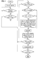
- is a flow chart showing a spare column allocation method in accordance with an embodiment of the invention,
- Fig. 5
- is a flow chart showing a spare row allocation method in accordance with an embodiment of the invention,
- Fig. 6
- is a flow chart showing a test/repair sequence in accordance with an embodiment of the invention,
- Fig. 7
- shows a schematic view of an example of a memory array with faulty cells, and
- Fig. 8
- shows the memory of Fig. 7 after repair.
- Circuit infrastructure needed to implement a spare row/column allocation as part of an embodiment of the method according to the invention is shown in Figs. 1 and 2, wherein Fig. 2 is a more detailed representation of a Column Memory Built-In Self Repair (MBISR)
circuit 3, which Column Memory Built-In Self Repair (MBISR)circuit 3 is part of the scheme of Fig. 1. Each memory array 2 (cf. also Fig. 3) with a given amount of spare rows and columns is provided with two independent spare row/column allocation circuits (Memory Built-In Self Repair (MBISR),circuits) 3, i.e. one Column Memory Built-In Self Repair (MBISR) circuit (cf. Fig. 2), and one Row Memory Built-In Self Repair (MBISR) circuit. It.has to be understood that in the present example the principle structures of the Column Memory Built-In Self Repair (MBISR) circuit and of the Row Memory Built-In Self Repair (MBISR) circuit are the same. Hence, the detailed scheme of Fig. 2 showing an embodiment of the Column Memory Built-In Self Repair (MBISR) circuit applies to an embodiment of the Row Memory Built-In Self Repair (MBISR) circuit in the present example, respectively. - Each of the row/
column allocation circuits 3 contains a set of faulty row/column registers which point to the rows and columns to be replaced, a comparator/decoder 11 which selects the faulty row/column registers to compare or write to during the memory tests, and a control logic which synchronizes the operation with the different test phases (row or column test) and provides the interface to non volatile faulty row/column storage elements (fuses). - Fig. 3 shows an overall diagram of a memory unit 5 made of multiple memories with row/
column redundancies 2, each provided with adedicated MBISR 3, and a sharedword redundancy block 4. The memory unit 5 is connected to a standard Memory Built-In Self Test controller (MBIST) 8 and a bank of non volatile storage elements (fuses) 12 serving allMBISRs 3 and theword redundancy block 4. - In more detail, each
MBISR 3 as shown in Fig. 3 consists of one Column Memory Built-In Self Repair (MBISR) circuit and one Row Memory Built-In Self Repair (MBISR) circuit as to be seen in Fig. 1. I.e., the memory unit 5 of Fig. 3 carries six single schemes of the type shown in Fig. 1. - The embodiment of a Memory Built-In Self Repair (MBISR) device as shown in Fig. 3 is an embodiment of the Memory Built-In Self Repair (MBISR) device according to
claim 9 and concurrently an embodiment of the Memory Built-In Self Repair (MBISR) device according to claim 28. Alternate configurations of embodiments of the Memory Built-In Self Repair (MBISR) device according to claim 28 alone may contain only one set of row/column allocation circuits shared by allmemory arrays 2 with spare rows and columns. - The spare row/column allocation method according to the present example is based on the simple rule that spare rows and columns must replace array rows and columns with the highest number of faulty cells; faulty cells not covered by row/column redundancy, if any, will be replaced by redundant words as long as they are available, otherwise a FAIL signal is activated to flag that the
memory 2 is not repairable. - As a prerequisite, the tester must check an entire row or column at a time and not portions of them.
- Row and column tests can be executed in any order, depending on which detection and repair strategy best fits the most frequent defects for any given memory technology.
- In this example it is assumed that spare column allocation is calculated first; the method is shown in the flow diagram of Fig. 4.
- Once started, all faulty column registers Col address register(i) (cf. Fig. 1), NFC(i) (see below), Row address register(k) and NFR(k) (see below) are cleared; calculation stands by as long as the
memory 2 is not selected or no column test is being performed, thus limiting the overall testing power consumption. - During column tests, a column adress buffer (Col address buffer) 9 (cf. Fig. 1) stores the address of the last column accessed; a Number of Faults in Column register (NFC) (cf. Fig. 1) is incremented each time a fault in the column pointed by the
Col address buffer 9 is detected, thus storing the number of faulty cells belonging to that column. - Whenever the column address changes, the value stored in the NFC register is compared with a fixed first threshold beyond which it is considered worth to replace an entire column in the cell array; if there are too few faulty cells in a column, that may be even fixed by using redundant words or wordlines instead, the NFC register is cleared and calculation restarts from the next column being tested (if the first threshold value is set to 0, a spare column might be used to fix an array column with at least 1 defective cell).
- The value of the column replacement threshold, i.e. the first threshold, is stored in a column threshold register 13 (see figure 1).
- Should the first threshold be exceeded, the current value in the NFC register is compared to those stored in NFC(i) registers of a faulty columns register
array 7, where the index i ranges from 1 to the number n of available spare columns (see Fig. 1). - If there is at least one value of i for which it results NFC>NFC(i), i.e. the value stored in the NFC register is greater than at least one of those stored in the NFC(i) registers, then the values in the
Col address buffer 9 and NFC registers are copied to the Col address register(j) and NFC(j) pair with the lowest value NFC(j) among all current NFC(i), an Activation Flag AF(j) being (re)asserted to indicate that the Col address register(j) register contains an effective faulty column address (cf. Fig. 1). - Once the Activation Flag AF(j) is asserted, the corresponding spare column is activated and the faulty array column is replaced therefore there will be no more faults detected at that column until the values at Col address register(j) and NFC(j) are overwritten; spare columns are dynamically assigned to faulty array columns at test runtime, this prevents the same faulty column from being pointed by more than one Col address register(i)/NFC(i) pair (which would happen if the test scans all columns multiple times and in different orders).
- The same method applies to spare row allocation (Fig. 5): during row tests, a
Row address buffer 10 points to the last row accessed; a Number of Faults in Row (NFR) register (cf. Fig. 1) is incremented each time a fault in the row pointed by theRow address buffer 10 is detected, thus storing the number of faulty cells belonging to that row. - Whenever the row address changes, the value stored in the NFR register is compared with a fixed second threshold beyond which it is considered worth to replace an entire row in the cell array; if there are too few faulty cells in a row, that may be even fixed by using redundant words instead, the NFR register is cleared and calculation restarts from the next row being tested (if the second threshold value is set to 0, a spare row might be used to fix an array row with at least 1 defective cell).
- The value of the row replacement threshold, i.e. the second threshold, is stored in a row threshold register 14 (see Fig. 1).
- Should the second threshold be exceeded, the current value in the NFR register is compared to those stored in the NFR(k) registers of a faulty rows register
array 15, where the index k ranges from l to the number m of available spare rows (cf. Fig. 1). - If there is at least one value of k for which it results NFR>NFR(k), i.e. the value stored in the NFR register is greater than at least one of those stored in the NFR(k) registers, then the values in the
Row address buffer 10 and NFR registers are copied to the Row address register (l) and NFR (l) pair with the lowest value NFR (l) among all current NFR (k); an Activation Flag AF (l) being (re)asserted to indicate that the Row address register (l) register contains an effective faulty row address. - Once the Activation Flag AF (l) is asserted, the corresponding spare row is activated and the faulty array row is replaced, therefore there will be no more faults detected at that row until the values at Row address register (l) and NFR (l) are overwritten; spare rows are dynamically assigned to faulty array rows at test runtime, this prevents the same faulty row from being pointed by more than one Row address register(k)/NFR(k) pair (which would happen if the test scans all rows multiple times and in different orders).
- The main advantage of this method consists of handling only the number of faulty cells per row/column, regardless of how these cells are distributed within rows, columns and words; the repair strategy aims to fix as much faulty cells as possible by means of spare rows and columns, any additional unfixed cells being replaced with redundant words.
- Values in the faulty row/column registers can be stored in any order.
- Each time the current values of Col address buffer/NFC or Row address buffer/NFR must be stored into the faulty row/column registers, the pair with the lowest value of NFC(j) or NFR (l) is overwritten; the number of faulty row/column registers is fixed (equal to the number of spare rows/columns) and does not depend from the size of the
memory 2. - Once finished, the highest fault counts will be stored in the NFC(i) and NFR(k) registers along with the row/column addresses they refer to; registers Col address register (i) and Row address register(k) are used to activate spare columns and rows, respectively, thus maximizing the number of faulty cells which can be repaired using these redundancies.
- As the algorithm simply overwrites faulty row/column registers as needed, no additional logic is neither needed to check whether free registers are available nor whether the current row/column address is already stored into the faulty row/column registers.
- Fig. 6 shows an example of a memory test/repair sequence in accordance with the invention (column test is executed first).
- When detected, faulty array columns are replaced at test runtime; this prevents row test from detecting the same faults detected by column test.
- During row test, faulty array rows are replaced by spare rows; if no faulty row is detected then the test to detect faulty words is skipped, thus saving testing time (there is no need to test memory words if no faulty wordline was found), otherwise memory word test is executed afterwards.
- Detected faulty words (i.e. memory words with at least one faulty cell) are repaired by activating redundant words as long as spare words are available; should no more spare word be available, signal FAIL is activated to flag that the memory is not repairable and execution ends, otherwise all memory faults are repaired (additional memory tests may optionally be performed to check that no faults are detected after completion of the test/repair sequence).
- A memory array sample is shown schematically in Fig. 7: for simplicity it is assumed that the physical and the logical organization of the cell array are the same, i.e. arranged into 36 rows (R0 to R35) and 28 columns (C0 to C27); each subsequent group of 4 columns forms one memory word, therefore each row is logically splitted into 7 words of 4 cells each (W0 to W6).
- The method applies to real array structures as well, for which memory word bits are interleaved.
- The array is provided with 2 spare rows and 2 spare columns, therefore each spare allocation circuit will contain two Col/Row address buffer/NFR/NFC pairs; in addition, there are 4 spare words that can be shared among all the arrays in the memory unit.
- Both column and row thresholds are set to 2, that means that a spare column or row is used to repair columns and rows with at least 3 faulty cells.
- The memory is tested according to the sequence as described above with reference to Fig. 6, with rows being scanned from R0 to R35 and columns from C0 to C27; column test is executed first.
- Once started the column test, all faulty column registers are set to 0:
- Col address register 0 = 0; NFC 0 = 0
- Col address register 1 = 0;
NFC 1 = 0 - Due to the threshold value set to 2, faulty column registers are not updated until column C16 is reached; as C16 contains 6 faulty cells (see Fig. 7), faulty column registers are updated as shown below (in case of more of one registers containing the lowest value, it can be assumed that the one with the lower index is overwritten):
- Col address register 0 = 16; NFC 0 = 6
- Col address register 1 = 0;
NFC 1 = 0 - As activation flag AF0 is set to 1, column C16 is replaced with a spare column; no further faults will be detected at column C16 unless the spare column is reassigned to another faulty column during the test.
- The test continues and no updates occur until C24, containing 11 faulty cells, is reached; the content of Col address buffer/NFC is compared to those of faulty column registers and, since it is greater than both, after the first comparison it is written to the faulty column register with the lowest value of NFC:
- Col address register 0 = 16; NFC 0 = 6
- Col address register 1 = 24;
NFC 1 = 11 - Again, flag AF1 is set to 1 and column C24 is replaced with the second spare column available.
- The test proceeds until C27, as no further updates occur, array columns C16 and C24 are replaced according to values stored into Col address register 0 and
Col address register 1. Once faulty columns are repaired, the row test is started; generally, rows are tested on a by word basis, i.e. the number of faults per row equals the number of words on the same row containing at least one failing cell. - Once started the row test, all faulty row registers are set to 0:
- Row address register 0 = 0; NFR 0 = 0
-
Row address register 1 = 0;NFR 1 = 0 - No faulty row registers updates occur until row R1, containing 6 faulty words (see Fig. 7), is reached; the faulty row is stored into faulty row registers as shown below:
- Row address register 0 = 1; NFR 0 = 6
-
Row address register 1 = 0;NFR 1 = 0 - As activation flag AF0 is set to 1, row R1 is replaced with a spare row; no further faults will be detected at row R1 unless the spare row is reassigned to another faulty row during the test.
- Due to the row threshold set to 2, the next update occurs at row R9, containing 3 faulty words; the faulty row register with the lowest value of NFR is updated:
- Row address register 0 = 1; NFR 0 = 6
-
Row address register 1 = 9;NFR 1 = 3 - Flag AF1 is set to 1 and row R9 is replaced with the second spare row available.
- Then, 7 faulty words are detected at row R20; as 7 is greater than either the values at NFR 0 and
NFR 1, the faulty row register with the lowest value of NFR (i.e. NFR 1) is again updated: - Row address register 0 = 1; NFR 0 = 6
-
Row address register 1 = 20;NFR 1 = 7 - The second spare row is reassigned to row R20 which contains more faulty cells.
- The test proceeds until R35; as no further updates occur, spare rows are activated to replace array rows R1 and R20 according to values stored into Row address register 0 and
Row address register 1. - At the end of row/column tests, Col/Row address buffers will point to rows and columns with the highest number of faults.
- Once faulty rows are repaired, the row test is started again and no faulty rows are detected except R9 which contains 3 faulty words; row R9 is repaired by means of 3 spare words, the fourth spare word being left unused.
- The memory array after repair is shown in Fig. 8; the result is independent from the scanning direction during tests.
- In the example shown, no repair would be possible if the spare row allocation algorithm would have replaced rows R1 and R9; if so, row R20 would have needed 7 redundant words to be repaired versus the 4 spare words available.
- Further, it is pointed out that although fuses represent a widely used example for non-volatile storage elements for storage of fault data, there are other non-volatile storage elements which could be used instead.
Claims (52)
- Method for repairing a memory comprising a Memory Built-In Self Repair (MBISR) structure, which method comprises the steps ofcharacterized in thatdetection of defective storage cells, andredundancy allocation,
the redundancy allocation step is carried out in such a way that it combines a row and/or column oriented redundancy repair approach with a word oriented redundancy repair approach. - Method according to claim 1, wherein the step of detection of defective storage cells comprises a column test, which column test comprises the following steps:and wherein, once the activation flag AF(j) is asserted or reasserted, respectively, a corresponding spare column is activated and the faulty array column is replaced.a) storing the address of the column accessed in a column address buffer,b) incrementing a Number of Faults in Column (NFC) register each time a fault in the column pointed by the column address buffer is detected,c) comparing the value stored in the NFC register with a predetermined first threshold after checking all cells in the column pointed by the column address buffer,d) if the value stored in the NFC register does not exceed the predetermined first threshold, then the column address buffer is pointed to a further column and the NFC register is cleared, otherwise the value stored in the NFC register is compared with values stored in NFC(i) registers of a faulty columns register array (7), wherein index i ranges from 1 to the number n of available spare columns, ande) if the value stored in the NFC register does not exceed at least one of the values stored in the NFC(i) registers, then the column address buffer is pointed to a further column and the NFC register is cleared, otherwise the values in the column address buffer and NFC registers are copied to the column address register(j) and NFC(j) pair with the lowest value NFC(j) among all current NFC(i), and an activation flag AF(j) is asserted or reasserted, respectively, to indicate that the column address register(j) contains an effective faulty column address,
- Method according to any of the preceding claims, wherein the step of detection of defective storage cells comprises a row test, which row test comprises the following steps:and wherein, once the activation flag AF (l) is asserted or reasserted, respectively, a corresponding spare row is activated and the faulty array row is replaced.a) storing the address of the row accessed in a row address buffer,b) incrementing a Number of Faults in Rows (NFR) register each time a fault in the row pointed by the row address buffer is detected,c) comparing the value stored in the NFR register with a predetermined second threshold after checking all cells in the row pointed by the row address buffer,d) if the value stored in the NFR register does not exceed the predetermined second threshold, then the row address buffer is pointed to a further row and the NFR register is cleared, otherwise the value stored in the NFR register is compared with values stored in NFR(k) registers of a faulty rows register array (15), wherein index k ranges from 1 to the number m of available spare rows, ande) if the value stored in the NFR register does not exceed at least one of the values stored in the NFR(k) registers, then the row address buffer is pointed to a further row and the NFR register is cleared, otherwise the values in the row address buffer and NFR registers are copied to the row address register (l) and NFR (l) pair with the lowest value NFR (l) among all current NFR(k), and an activation flag AF (l) is asserted or reasserted, respectively, to indicate that the row address register (l) contains an effective faulty row address,
- Method according to any of the preceding claims, characterized in that the redundancy allocation step comprises the following steps:a) replacing array rows and/or columns comprising the highest number of faulty cells by spare rows and/or columns, andb) replacing faulty cells not covered by row/column redundancy, if any, by redundant words as long as they are available.
- Method according to claim 4, characterized in that it comprises the step of activating a FAIL signal to flag that the memory is not repairable, if defective cells remain after allocation of all redundant rows and/or columns and words.
- Method according to any of the preceding claims, characterized in that it comprises a Memory Built-In Self Test (MBIST).
- Method according to claim 6, characterized in that said Memory Built-In Self Test (MBIST) is one single Memory Built-In Self Test (MBIST) serving multiple memories with embedded and shared redundancies.
- Method according to claim 1, characterized in that said memory is a static memory or a dynamic memory.
- Memory Built-In Self Repair (MBISR) device (1) comprisingcharacterized in thata plurality of memories (2), each of said memories (2) having row and/or column redundancy, anda row and/or column Memory Built-In Self Repair circuit (3),
said Memory Built-In Self Repair (MBISR) device (1) comprises further row and/or column Memory Built-In Self Repair (MBISR) circuits (3), wherein all said row and/or column Memory Built-In Self Repair (MBISR) circuits (3) of said Memory Built-In Self Repair (MBISR) device are arranged such that each row and/or column Memory Built-In Self Repair (MBISR) circuit (3) belongs to one and only one of said memories (2) and each of said memories (2) is provided with at least one of said row and/or column Memory Built-In Self Repair (MBISR) circuits (3). - Memory Built-In Self Repair (MBISR) device (1) according to claim 9, characterized in that each of said memories (2) is provided with one and only one row Memory Built-In Self Repair (MBISR) circuit (3) and with one and only one column Memory Built-In Self Repair (MBISR) circuit (3).
- Memory Built-In Self Repair (MBISR) device (1) according to claim 9 or claim 10, characterized in that it further comprises a word redundancy block (4).
- Memory Built-In Self Repair (MBISR) device (1) according to claim 11, characterized in that some or all of said memories (2) share said word redundancy block (4).
- Memory Built-In Self Repair (MBISR) device (1) according to any of claims 9 to 12, characterized in that said plurality of memories (2) comprises dynamic memories and / or static memories.
- Memory Built-In Self Repair (MBISR) device (1) according to any of claims 9 to 13, characterized in that it further comprises an address decoder / output multiplexer unit (6), which address decoder output multiplexer unit (6) is coupled to each of said Memory Built-In Self Repair (MBISR) circuits (3) and memories
- Memory Built-In Self Repair (MBISR) device (1) according to claim 14, characterized in thatsaid plurality of memories (2) and said address decoder / output multiplexer unit (6) are arranged such that they form a memory unit (5), andit comprises a Memory Built-In Self Test (MBIST) controller (8) connected to said memory unit (5).
- Memory Built-In Self Repair (MBISR) device (1) according to claim 15, characterized in that the Memory Built-In Self Test (MBIST) controller (8) is arranged such that it checks an entire row or column at a time.
- Memory Built-In Self Repair (MBISR) device (1) according to claim 15, referring back to claim 11 or to claim 12 via claim 14, characterized in that said word redundancy block (4) is part of said memory unit (5).
- Memory Built-In Self Repair (MBISR) device (1) according to any of claims 11, 12 or 17, characterized by a bank of non volatile storage elements (12) serving all Memory Built-In Self Repair (MBISR) circuits (3) and the word redundancy block (4).
- Memory Built-In Self Repair (MBISR) device (1) according to any of claims 11, 12, 17 or 18, characterized in that it is arranged such that it carries out redundancy allocation in such a way that it combines a row and/or column oriented redundancy repair approach with a word oriented redundancy repair approach.
- Memory Built-In Self Repair (MBISR) device (1) according to claim 19, characterized in that it is arranged such that it carries out redundancy allocation with the following steps:a) replacing array rows and/or columns comprising the highest number of faulty cells by spare rows and/or columns, andb) replacing faulty cells not covered by row/column redundancy, if any, by redundant words as long as they are available.
- Memory Built-In Self Repair (MBISR) device (1) according to claim 20, characterized in that it is arranged such that it activates a FAIL signal to flag that the memory is not repairable, if defective cells remain after allocation of all redundant rows and/or columns and words.
- Memory Built-In Self Repair (MBISR) device (1) according to any of claims 9 to 21, characterized in that at least one Memory Built-In Self Repair (MBISR) circuit (3) comprisesa column address buffer (9),n registers (NFC(i)) for storing Number of Faults in Column values, wherein n is the number of available spare columns in the memory (2) belonging to said Memory Built-In Self Repair (MBISR) circuit (3),n column address registers(j) arranged in a faulty columns register array (7), anda further register (NFC) for storing the Number of Faults in Column being tested.
- Memory Built-In Self Repair (MBISR) device (1) according to claim 22, characterized in that said at least one Memory Built-In Self Repair (MBISR) circuit (3) further comprisesa column threshold register (13),a comparator and decoder unit (11) arranged such that it gets input from the registers (NFC(i)) for storing Number of Faults in Column values, from said further register (NFC) for storing the Number of Faults in Column being tested, and from the column threshold register (13), and that it outputs signals to the faulty columns register array (7), anda control logic unit for controlling operation of the Column Memory Built-In Self Repair (MBISR) circuit (3).
- Memory Built-In Self Repair (MBISR) device (1) according to claim 22 or claim 23, characterized in that it is arranged such that it carries out a defective storage cell detection and redundancy allocation process comprising the following steps:a) storing the address of the column accessed in the column address buffer (9),b) incrementing said further Number of Faults in Column (NFC) register each time a fault in the column pointed by the column address buffer (9) is detected,c) comparing the value stored in the NFC register with a predetermined first threshold after checking all cells in the column pointed by the column address buffer (9),d) if the value stored in the NFC register does not exceed the predetermined first threshold, then pointing the column address buffer (9) to a further column and clearing the NFC register, otherwise comparing the value stored in the NFC register with values stored in the NFC(i) registers,e) if the value stored in the NFC register does not exceed at least one of the values stored in the NFC(i) registers, then pointing the column address buffer (9) to a further column and clearing the NFC register, otherwise copying the values in the column address buffer (9) and NFC registers to the column address register(j) and NFC(j) pair with the lowest value NFC(j) among all current NFC(i), and asserting or reasserting, respectively, an activation flag AF(j) to indicate that the column address register(j) contains an effective faulty column address, andf) once the activation flag AF(j) is asserted or reasserted, respectively, activating a corresponding spare column to replace the faulty array column.
- Memory Built-In Self Repair (MBISR) device (1) according to any of claims 9 to 24, characterized in that at least one Memory Built-In Self Repair (MBISR) circuit (3) comprisesa row address buffer (10),m registers (NFR(k)) for storing Number of Faults in Row values, wherein m is the number of available spare rows in the memory (2) belonging to said Memory Built-In Self Repair (MBISR) circuit (3),m row address registers (l) arranged in a faulty rows register array (15), anda further register (NFR) for storing the Number of Faults in Row being tested.
- Memory Built-In Self Repair (MBISR) device (1) according to claim 25, characterized in that said at least one Memory Built-In Self Repair (MBISR) circuit (3) further comprisesa row threshold register (14),a comparator and decoder unit (11) arranged such that it gets input from the registers (NFR(k)) for storing Number of Faults in Row values, from said further register (NFR) for storing the Number of Faults in Row being tested, and from the row threshold register (14), and that it outputs signals to the faulty rows register array (15), anda control logic unit for controlling operation of the Row Memory Built-In Self Repair (MBISR) circuit (3).
- Memory Built-In Self Repair (MBISR) device (1) according to claim 25 or claim 26, characterized in that it is arranged such that it carries out a defective storage cell detection and redundancy allocation process comprising the following steps:a) storing the address of the row accessed in the row address buffer (10),b) incrementing said further Number of Faults in Row (NFR) register each time a fault in the row pointed by the row address buffer (10) is detected,c) comparing the value stored in the NFR register with a predetermined second threshold after checking all cells in the row pointed by the row address buffer (10),d) if the value stored in the NFR register does not exceed the predetermined second threshold, then pointing the row address buffer (10) to a further row and clearing the NFR register, otherwise comparing the value stored in the NFR register with values stored in the NFR(k) registers,e) if the value stored in the NFR register does not exceed at least one of the values stored in the NFR(k) registers, then pointing the row address buffer (10) to a further row and clearing the NFR register, otherwise copying the values in the row address buffer (10) and NFR registers to the row address register (l) and NFR(l) pair with the lowest value NFR(l) among all current NFR(k), and asserting or reasserting, respectively, an activation flag AF(l) to indicate that the row address register (l) contains an effective faulty row address, andf) once the activation flag AF (l) is asserted or reasserted, respectively, activating a corresponding spare row to replace the faulty array row.
- Memory Built-In Self Repair (MBISR) device (1) comprisingcharacterized in that said Memory Built-In Self Repair (MBISR) device (1) further comprises a word redundancy block (4).a memory (2) with row and/or column redundancy, andat least one row and/or column Memory Built-In Self Repair (MBISR) circuit (3),
- Memory Built-In Self Repair (MBISR) device (1) according to claim 28, characterized in that said memory (2) is a static memory or a dynamic memory.
- Memory Built-In Self Repair (MBISR) device (1) according to claim 28 or claim 29, characterized in that it comprises a plurality of memories (2) forming a memory unit (5), whereineach of said memories (2) comprises row and/or column redundancy,each of said memories (2) is provided with a dedicated Memory Built-In Self Repair (MBISR) circuit (3), andsome or all of said memories (2) share said word redundancy block (4).
- Memory Built-In Self Repair (MBISR) device according to claim 28 or claim 29, characterized in that it comprises a plurality of memories forming a memory unit, whereineach of said memories comprises row and/or column redundancy,some or all of said memories are provided with a row and/or column Memory Built-In Self Repair (MBISR) circuit, wherein at least one row and/or column Memory Built-In Self Repair (MBISR) circuit is shared by at least two of said memories, andsome or all of said memories share said word redundancy block.
- Memory Built-In Self Repair (MBISR) device according to claim 31, characterized in that all said memories share one and the same Memory Built-In Self Repair (MBISR) circuit.
- Memory Built-In Self Repair (MBISR) device (1) according to any of claims 30 to 32, characterized in that all said memories (2) share one and the same word redundancy block (4).
- Memory Built-In Self Repair (MBISR) device (1) according to any of claims 30 to 33, characterized in that said memory unit (5) comprises an address decoder / output multiplexer unit (6), which address decoder / output multiplexer unit (6) is coupled to each of said Memory Built-In Self Repair (MBISR) circuits (3) and memories (2).
- Memory Built-In Self Repair (MBISR) device according to any of claims 28 to 34, characterized by a bank of non volatile storage elements (12) serving all Memory Built-In Self Repair (MBISR) circuits (3) and the word redundancy block (4).
- Memory Built-In Self Repair (MBISR) device according to any of claims 28 to 35, characterized by a Memory Built-In Self Test (MBIST) controller (8) connected to said memory (2) or to said memory unit (5), respectively.
- Memory Built-In Self Repair (MBISR) device according to claim 36, characterized in that the Memory Built-In Self Test (MBIST) controller (8) is arranged such that it checks an entire row or column at a time.
- Memory Built-In Self Repair (MBISR) device according to any of claims 28 to 37, characterized in that it is arranged such that it carries out redundancy allocation in such a way that it combines a row and/or column oriented redundancy repair approach with a word oriented redundancy repair approach.
- Memory Built-In Self Repair (MBISR) device according to any of claims 28 to 38, characterized in that at least one Memory Built-In Self Repair (MBISR) circuit (3) comprisesa column address buffer (9),n registers (NFC(i)) for storing Number of Faults in Column values, wherein n is the number of available spare columns in the memory (2) belonging to said Memory Built-In-Self Repair (MBISR) circuit (3),n column address registers(j) arranged in a faulty columns register array (7), anda further register (NFC) for storing the Number of Faults in Column being tested.
- Memory Built-In Self Repair (MBISR) device according to claim 39, characterized in that said at least one Memory Built-In Self Repair (MBISR) circuit (3) further comprisesa column threshold register (13),a comparator and decoder unit (11) arranged such that it gets input from the registers (NFC(i)) for storing Number of Faults in Column values, from said further register (NFC) for storing the Number of Faults in Column being tested, and from the column threshold register (13), and that it outputs signals to the faulty columns register array (7), anda control logic unit for controlling operation of the Column Memory Built-In Self Repair (MBISR) circuit (3).
- Memory Built-In Self Repair (MBISR) device according to claim 39 or claim 40, characterized in that it is arranged such that it carries out a defective storage cell detection and redundancy allocation process comprising the following steps:a) storing the address of the column accessed in the column address buffer (9),b) incrementing said further Number of Faults in Column (NFC) register each time a fault in the column pointed by the column address buffer (9) is detected,c) comparing the value stored in the NFC register with a predetermined first threshold after checking all cells in the column pointed by the column address buffer (9),d) if the value stored in the NFC register does not exceed the predetermined first threshold, then pointing the column address buffer (9) to a further column and clearing the NFC register, otherwise comparing the value stored in the NFC register with values stored in the NFC(i) registers,e) if the value stored in the NFC register does not exceed at least one of the values stored in the NFC(i) registers, then pointing the column address buffer (9) to a further column and clearing the NFC register, otherwise copying the values in the column address buffer (9) and NFC registers to the column address register(j) and NFC(j) pair with the lowest value NFC(j) among all current NFC(i), and asserting or reasserting, respectively, an activation flag AF(j) to indicate that the column address register(j) contains an effective faulty column address, andf) once the activation flag AF(j) is asserted or reasserted, respectively, activating a corresponding spare column to replace the faulty array column.
- Memory Built-In Self Repair (MBISR) device according to any of claims 28 to 41, characterized in that at least one Memory Built-In Self Repair (MBISR) circuit (3) comprisesa row address buffer (10),m registers (NFR(k)) for storing Number of Faults in Row values, wherein m is the number of available spare rows in the memory (2) belonging to said Memory Built-In Self Repair (MBISR) circuit (3),m row address registers(l) arranged in a faulty rows register array (15), anda further register (NFR) for storing the Number of Faults in Row being tested.
- Memory Built-In Self Repair (MBISR) device according to claim 42, characterized in that said at least one Memory Built-In Self Repair (MBISR) circuit (3) further comprisesa row threshold register (14),a comparator and decoder unit (11) arranged such that it gets input from the registers (NFR(k)) for storing Number of Faults in Row values, from said further register (NFR) for storing the Number of Faults in Row being tested, and from the row threshold register (14), and that it outputs signals to the faulty rows register array (15), anda control logic unit for controlling operation of the Row Memory Built-In Self Repair (MBISR) circuit (3).
- Memory Built-in Self Repair (MBISR) device according to claim 42 or claim 43, characterized in that it is arranged such that it carries out a defective storage cell detection and redundancy allocation process comprising the following steps:a) storing the address of the row accessed in the row address buffer (10),b) incrementing said further Number of Faults in Row (NFR) register each time a fault in the row pointed by the row address buffer (10) is detected,c) comparing the value stored in the NFR register with a predetermined second threshold after checking all cells in the row pointed by the row address buffer (10),d) if the value stored in the NFR register does not exceed the predetermined second threshold, then pointing the row address buffer (10) to a further row and clearing the NFR register, otherwise comparing the value stored in the NFR register with values stored in the NFR(k) registers,e) if the value stored in the NFR register does not exceed at least one of the values stored in the NFR(k) registers, then pointing the row address buffer (10) to a further row and clearing the NFR register, otherwise copying the values in the row address buffer (10) and NFR registers to the row address registe (l) and NFR(l) pair with the lowest value NFR(l) among all current NFR(k), and asserting or reasserting, respectively, an activation flag AF(l) to indicate that the row address register(l) contains an effective faulty row address, andf) once the activation flag AF(l) is asserted or reasserted, respectively, activating a corresponding spare row to replace the faulty array row.
- Memory Built-In Self Repair (MBISR) device according to any of claims 28 to 44, characterized in that it is arranged such that it carries out redundancy allocation with the following steps:a) replacing array rows and/or columns comprising the highest number of faulty cells by spare rows and/or columns, andb) replacing faulty cells not covered by row/column redundancy, if any, by redundant words as long as they are available.
- Memory Built-In Self Repair (MBISR) device according to claim 45, characterized in that it is arranged such that it activates a FAIL signal to flag that the memory is not repairable, if defective cells remain after allocation of all redundant rows and/or columns and words.
- Column Memory Built-In Self Repair (MBISR) circuit (3) characterized in that it comprisesa column address buffer (9),n registers (NFC(i)) for storing Number of Faults in Column values, wherein n is the number of available spare columns in a memory (2) belonging to said Column Memory Built-In Self Repair (MBISR) circuit (3),n column address registers(j) arranged in a faulty columns register array (7), anda further register (NFC) for storing the Number of Faults in Column being tested.
- Column Memory Built-In Self Repair (MBISR), circuit (3) according to claim 47, characterized in that it further comprisesa column threshold register (13),a comparator and decoder unit (11) arranged such that it gets input from the registers (NFC(i)) for storing Number of Faults in Column values, from said further register (NFC) for storing the Number of Faults in Column being tested, and from the column threshold register (13), and that it outputs signals to the faulty columns register array (7), anda control logic unit for controlling operation of the Column Memory Built-In Self Repair (MBISR) circuit (3).
- Column Memory Built-In Self Repair (MBISR) circuit (3) according to claim 47 or claim 48, characterized in that it is arranged such that it carries out a defective storage cell detection and redundancy allocation process comprising the following steps:a) storing the address of the column accessed in the column address buffer (9),.b) incrementing said further Number of Faults in Column (NFC) register each time a fault in the column pointed by the column address buffer (9) is detected,c) comparing the value stored in the NFC register with a predetermined first threshold after checking all cells in the column pointed by the column address buffer (9),d) if the value stored in the NFC register does not exceed the predetermined first threshold, then pointing the column address buffer (9) to a further column and clearing the NFC register, otherwise comparing the value stored in the NFC register with values stored in the NFC(i) registers,e) if the value stored in the NFC register does not exceed at least one of the values stored in the NFC(i) registers, then pointing the column address buffer (9) to a further column and clearing the NFC register, otherwise copying the values in the column address buffer (9) and NFC registers to the column address register(j) and NFC(j) pair with the lowest value NFC(j) among all current NFC(i), and asserting or reasserting, respectively, an activation flag AF(j) to indicate that the column address register(j) contains an effective faulty column address, andf) once the activation flag AF(j) is asserted or reasserted, respectively, activating a corresponding spare column to replace the faulty array column.
- Row Memory Built-In Self Repair (MBISR) circuit (3),
characterized in that it comprisesa row address buffer (10),m registers (NFR(k)) for storing Number of Faults in Row values, wherein m is the number of available .spare rows in a memory (2) belonging to said Memory Built-In Self Repair (MBISR) circuit (3),m row address registers (1) arranged in a faulty rows register array (15), anda further register (NFR) for storing the Number of Faults in Row being tested. - Row Memory Built-In Self Repair (MBISR) circuit (3) according to claim 50, characterized in that it further comprisesa row threshold register (14),a comparator and decoder unit (11) arranged such that it gets input from the registers (NFR(k)) for storing Number of Faults in Row values, from said further register (NFR) for storing the Number of Faults in Row being tested, and from the row threshold register (14), and that it outputs signals to the faulty rows register array (15), anda control logic unit for controlling operation of the Row Memory Built-In Self Repair (MBISR) circuit (3).
- Row Memory Built-In Self Repair (MBISR) circuit (3) according to claim 50 or claim 51, characterized in that it is arranged such that it carries out a defective storage cell detection and redundancy allocation process comprising the following steps:a) storing the address of the row accessed in the row address buffer (10),b) incrementing said further Number of Faults in Row (NFR) register each time a fault in the row pointed by the row address buffer (10) is detected,c) comparing the value stored in the NFR register with a predetermined second threshold after checking all cells in the row pointed by the row address buffer (10),d) if the value stored in the NFR register does not exceed the predetermined second threshold, then pointing the row address buffer (10) to a further row and clearing the NFR register, otherwise comparing the value stored in the NFR register with values stored in the NFR(k) registers,e) if the value stored in the NFR register does not exceed at least one of the values stored in the NFR(k) registers, then pointing the row address buffer (10) to a further row and clearing the NFR register, otherwise copying the values in the row address buffer (10) and NFR registers to the row address register(l) and NFR(l) pair with the lowest value NFR(l) among all current NFR(k), and asserting or reasserting, respectively, an activation flag AF(l) to indicate that the row address register(l) contains an effective faulty row address, andf) once the activation flag AF(l) is asserted or reasserted, respectively, activating a corresponding spare row to replace the faulty array row.
Priority Applications (4)
| Application Number | Priority Date | Filing Date | Title |
|---|---|---|---|
| DE60320745T DE60320745D1 (en) | 2003-02-12 | 2003-02-12 | Process and Memory Built-In Self Repair (MBISR) to repair a memory |
| EP04007688A EP1465204A3 (en) | 2003-02-12 | 2003-02-12 | Memory built-in self repair (MBISR) circuits / devices |
| EP03002698A EP1447813B9 (en) | 2003-02-12 | 2003-02-12 | Memory built-in self repair (MBISR) circuits / devices and method for repairing a memory comprising a memory built-in self repair (MBISR) structure |
| US10/777,025 US7627792B2 (en) | 2003-02-12 | 2004-02-11 | Memory built-in self repair (MBISR) circuits/devices and method for repairing a memory comprising a memory built-in self repair (MBISR) structure |
Applications Claiming Priority (1)
| Application Number | Priority Date | Filing Date | Title |
|---|---|---|---|
| EP03002698A EP1447813B9 (en) | 2003-02-12 | 2003-02-12 | Memory built-in self repair (MBISR) circuits / devices and method for repairing a memory comprising a memory built-in self repair (MBISR) structure |
Related Child Applications (1)
| Application Number | Title | Priority Date | Filing Date |
|---|---|---|---|
| EP04007688A Division EP1465204A3 (en) | 2003-02-12 | 2003-02-12 | Memory built-in self repair (MBISR) circuits / devices |
Publications (3)
| Publication Number | Publication Date |
|---|---|
| EP1447813A1 true EP1447813A1 (en) | 2004-08-18 |
| EP1447813B1 EP1447813B1 (en) | 2008-05-07 |
| EP1447813B9 EP1447813B9 (en) | 2008-10-22 |
Family
ID=32668951
Family Applications (2)
| Application Number | Title | Priority Date | Filing Date |
|---|---|---|---|
| EP04007688A Withdrawn EP1465204A3 (en) | 2003-02-12 | 2003-02-12 | Memory built-in self repair (MBISR) circuits / devices |
| EP03002698A Expired - Lifetime EP1447813B9 (en) | 2003-02-12 | 2003-02-12 | Memory built-in self repair (MBISR) circuits / devices and method for repairing a memory comprising a memory built-in self repair (MBISR) structure |
Family Applications Before (1)
| Application Number | Title | Priority Date | Filing Date |
|---|---|---|---|
| EP04007688A Withdrawn EP1465204A3 (en) | 2003-02-12 | 2003-02-12 | Memory built-in self repair (MBISR) circuits / devices |
Country Status (3)
| Country | Link |
|---|---|
| US (1) | US7627792B2 (en) |
| EP (2) | EP1465204A3 (en) |
| DE (1) | DE60320745D1 (en) |
Cited By (8)
| Publication number | Priority date | Publication date | Assignee | Title |
|---|---|---|---|---|
| EP1517334A1 (en) | 2003-09-16 | 2005-03-23 | Infineon Technologies AG | On-chip diagnosis method and on-chip diagnosis block for memory repair with mixed redundancy (IO redundancy and word-register redundancy) |
| US7350119B1 (en) * | 2004-06-02 | 2008-03-25 | Advanced Micro Devices, Inc. | Compressed encoding for repair |
| WO2009126812A1 (en) * | 2008-04-09 | 2009-10-15 | Inapac Technology, Inc. | Programmable memory repair scheme |
| US7644323B2 (en) * | 2004-11-30 | 2010-01-05 | Industrial Technology Research Institute | Method and apparatus of build-in self-diagnosis and repair in a memory with syndrome identification |
| EP1647031B1 (en) * | 2003-07-21 | 2010-03-10 | Infineon Technologies AG | Memory device and method of storing fail addresses of a memory cell |
| CN111798912A (en) * | 2019-04-04 | 2020-10-20 | 格芯公司 | Memory Built-in Self-Test Error Correction Code (MBIST ECC) for Low Voltage Memory |
| WO2021244917A1 (en) | 2020-05-30 | 2021-12-09 | Oerlikon Textile Gmbh & Co. Kg | Gear pump for metered delivery of color coatings |
| CN115877171A (en) * | 2021-09-28 | 2023-03-31 | 紫光同芯微电子有限公司 | Chip testing method and device |
Families Citing this family (21)
| Publication number | Priority date | Publication date | Assignee | Title |
|---|---|---|---|---|
| TWI252397B (en) * | 2004-09-17 | 2006-04-01 | Ind Tech Res Inst | Method and apparatus of built-in self-diagnosis and repair in a memory with syndrome identification |
| JP2006236551A (en) * | 2005-01-28 | 2006-09-07 | Renesas Technology Corp | Semiconductor integrated circuit having test function and manufacturing method |
| JP2006286141A (en) * | 2005-04-04 | 2006-10-19 | Toshiba Corp | Semiconductor memory device |
| KR100745403B1 (en) * | 2005-08-25 | 2007-08-02 | 삼성전자주식회사 | Semiconductor memory device and self test method |
| JP5554476B2 (en) * | 2008-06-23 | 2014-07-23 | ピーエスフォー ルクスコ エスエイアールエル | Semiconductor memory device and method for testing semiconductor memory device |
| US7839707B2 (en) * | 2008-09-09 | 2010-11-23 | Vitesse Semiconductor Corporation | Fuses for memory repair |
| US8010847B2 (en) * | 2008-09-30 | 2011-08-30 | Infineon Technologies Ag | Memory repair |
| US8127184B2 (en) * | 2008-11-26 | 2012-02-28 | Qualcomm Incorporated | System and method including built-in self test (BIST) circuit to test cache memory |
| US8446161B2 (en) * | 2009-03-17 | 2013-05-21 | Taiwan Semiconductor Manufacturing Company, Ltd. | Method of self monitoring and self repair for a semiconductor IC |
| US11119857B2 (en) * | 2012-09-18 | 2021-09-14 | Mosys, Inc. | Substitute redundant memory |
| US8719648B2 (en) | 2011-07-27 | 2014-05-06 | International Business Machines Corporation | Interleaving of memory repair data compression and fuse programming operations in single fusebay architecture |
| US8467260B2 (en) | 2011-08-05 | 2013-06-18 | International Business Machines Corporation | Structure and method for storing multiple repair pass data into a fusebay |
| US8484543B2 (en) | 2011-08-08 | 2013-07-09 | International Business Machines Corporation | Fusebay controller structure, system, and method |
| US8537627B2 (en) | 2011-09-01 | 2013-09-17 | International Business Machines Corporation | Determining fusebay storage element usage |
| US9734921B2 (en) * | 2012-11-06 | 2017-08-15 | Rambus Inc. | Memory repair using external tags |
| US10198314B2 (en) | 2013-05-23 | 2019-02-05 | Rambus Inc. | Memory device with in-system repair capability |
| KR20160022097A (en) | 2014-08-19 | 2016-02-29 | 삼성전자주식회사 | Semiconductor memory device and memory module having reconfiguration rejecting function |
| US10153055B2 (en) * | 2015-03-26 | 2018-12-11 | International Business Machines Corporation | Arbitration for memory diagnostics |
| US10204698B2 (en) | 2016-12-20 | 2019-02-12 | Ampere Computing Llc | Method to dynamically inject errors in a repairable memory on silicon and a method to validate built-in-self-repair logic |
| TWI736252B (en) * | 2020-05-08 | 2021-08-11 | 大陸商珠海南北極科技有限公司 | Memory circuit and memory repair method thereof |
| CN116246685A (en) * | 2021-12-08 | 2023-06-09 | 三星电子株式会社 | Storage device outputting test results and method for testing same |
Citations (5)
| Publication number | Priority date | Publication date | Assignee | Title |
|---|---|---|---|---|
| US5808945A (en) * | 1996-02-21 | 1998-09-15 | Sony Corporation | Semiconductor memory having redundant memory array |
| US6026505A (en) * | 1991-10-16 | 2000-02-15 | International Business Machines Corporation | Method and apparatus for real time two dimensional redundancy allocation |
| US6141267A (en) * | 1999-02-03 | 2000-10-31 | International Business Machines Corporation | Defect management engine for semiconductor memories and memory systems |
| US20020108073A1 (en) * | 2001-02-02 | 2002-08-08 | Hughes Brian William | System for and method of operating a programmable column fail counter for redundancy allocation |
| US20020159305A1 (en) * | 2000-10-18 | 2002-10-31 | Samsung Electronics Co., Ltd. | Semiconductor device including built-in redundancy analysis circuit for simultaneously testing and analyzing failure of a plurality of memories and method for analyzing the failure of the plurality of memories |
Family Cites Families (21)
| Publication number | Priority date | Publication date | Assignee | Title |
|---|---|---|---|---|
| US5153880A (en) * | 1990-03-12 | 1992-10-06 | Xicor, Inc. | Field-programmable redundancy apparatus for memory arrays |
| US5161157A (en) * | 1990-03-12 | 1992-11-03 | Xicor, Inc. | Field-programmable redundancy apparatus for memory arrays |
| US5588115A (en) * | 1993-01-29 | 1996-12-24 | Teradyne, Inc. | Redundancy analyzer for automatic memory tester |
| GB2292236A (en) * | 1995-04-04 | 1996-02-14 | Memory Corp Plc | Improved partial memory engine |
| US6011734A (en) * | 1998-03-12 | 2000-01-04 | Motorola, Inc. | Fuseless memory repair system and method of operation |
| TW446955B (en) * | 1998-10-30 | 2001-07-21 | Siemens Ag | The read/write memory with self-testing device and its associated test method |
| JP4204685B2 (en) * | 1999-01-19 | 2009-01-07 | 株式会社ルネサステクノロジ | Synchronous semiconductor memory device |
| US6181614B1 (en) * | 1999-11-12 | 2001-01-30 | International Business Machines Corporation | Dynamic repair of redundant memory array |
| US6640321B1 (en) * | 2000-04-14 | 2003-10-28 | Lsi Logic Corporation | Built-in self-repair of semiconductor memory with redundant row testing using background pattern |
| JP2001358296A (en) * | 2000-06-14 | 2001-12-26 | Mitsubishi Electric Corp | Semiconductor integrated circuit device |
| FR2811464B1 (en) * | 2000-07-05 | 2005-03-25 | St Microelectronics Sa | MEMORY CIRCUIT COMPRISING RESCUE CELLS |
| US6795942B1 (en) * | 2000-07-06 | 2004-09-21 | Lsi Logic Corporation | Built-in redundancy analysis for memories with row and column repair |
| US7178072B2 (en) * | 2001-06-08 | 2007-02-13 | Renesas Technology America, Inc. | Methods and apparatus for storing memory test information |
| US6862703B2 (en) * | 2001-08-13 | 2005-03-01 | Credence Systems Corporation | Apparatus for testing memories with redundant storage elements |
| US6973604B2 (en) * | 2002-03-08 | 2005-12-06 | Hewlett-Packard Development Company, L.P. | Allocation of sparing resources in a magnetoresistive solid-state storage device |
| US6879530B2 (en) * | 2002-07-18 | 2005-04-12 | Micron Technology, Inc. | Apparatus for dynamically repairing a semiconductor memory |
| US7003704B2 (en) * | 2002-11-12 | 2006-02-21 | International Business Machines Corporation | Two-dimensional redundancy calculation |
| DE10256487B4 (en) * | 2002-12-03 | 2008-12-24 | Infineon Technologies Ag | Integrated memory and method for testing an integrated memory |
| US20040123181A1 (en) * | 2002-12-20 | 2004-06-24 | Moon Nathan I. | Self-repair of memory arrays using preallocated redundancy (PAR) architecture |
| WO2004074851A2 (en) * | 2003-02-14 | 2004-09-02 | Logicvision Inc. | Memory repair analysis method and circuit |
| US6928377B2 (en) * | 2003-09-09 | 2005-08-09 | International Business Machines Corporation | Self-test architecture to implement data column redundancy in a RAM |
-
2003
- 2003-02-12 DE DE60320745T patent/DE60320745D1/en not_active Expired - Lifetime
- 2003-02-12 EP EP04007688A patent/EP1465204A3/en not_active Withdrawn
- 2003-02-12 EP EP03002698A patent/EP1447813B9/en not_active Expired - Lifetime
-
2004
- 2004-02-11 US US10/777,025 patent/US7627792B2/en not_active Expired - Fee Related
Patent Citations (5)
| Publication number | Priority date | Publication date | Assignee | Title |
|---|---|---|---|---|
| US6026505A (en) * | 1991-10-16 | 2000-02-15 | International Business Machines Corporation | Method and apparatus for real time two dimensional redundancy allocation |
| US5808945A (en) * | 1996-02-21 | 1998-09-15 | Sony Corporation | Semiconductor memory having redundant memory array |
| US6141267A (en) * | 1999-02-03 | 2000-10-31 | International Business Machines Corporation | Defect management engine for semiconductor memories and memory systems |
| US20020159305A1 (en) * | 2000-10-18 | 2002-10-31 | Samsung Electronics Co., Ltd. | Semiconductor device including built-in redundancy analysis circuit for simultaneously testing and analyzing failure of a plurality of memories and method for analyzing the failure of the plurality of memories |
| US20020108073A1 (en) * | 2001-02-02 | 2002-08-08 | Hughes Brian William | System for and method of operating a programmable column fail counter for redundancy allocation |
Non-Patent Citations (3)
| Title |
|---|
| BHAVSAR D K: "AN ALGORITHM FOR ROW-COLUMN SELF-REPAIR OF RAMS AND ITS IMPLEMENTATION IN THE ALPHA 21264", PROCEEDINGS INTERNATIONAL TEST CONFERENCE 1999. ITC'99. ATLANTIC CITY, NJ, SEPT. 28 - 30, 1999, INTERNATIONAL TEST CONFERENCE, NEW YORK, NY: IEEE, US, vol. CONF. 30, September 1999 (1999-09-01), pages 311 - 318, XP000928848, ISBN: 0-7803-5754-X * |
| GANAPATHY K N ET AL: "Yield modeling and optimization of large redundant RAMs", WAFER SCALE INTEGRATION, 1990. PROCEEDINGS., Y2ND INTERNATIONAL CONFERENCE ON SAN FRANCISCO, CA, USA 23-25 JAN. 1990, LOS ALAMITOS, CA, USA,IEEE COMPUT. SOC, US, 23 January 1990 (1990-01-23), pages 273 - 287, XP010033286, ISBN: 0-8186-9013-5 * |
| TARR M ET AL: "DEFECT ANALYSIS SYSTEM SPEEDS TEST AND REPAIR OF REDUNDANT MEMORIES", ELECTRONICS, VNU BUSINESS PUBLICATIONS, NEW YORK, US, vol. 57, no. 1, 12 January 1984 (1984-01-12), pages 175 - 179, XP000719133, ISSN: 0883-4989 * |
Cited By (25)
| Publication number | Priority date | Publication date | Assignee | Title |
|---|---|---|---|---|
| EP1647031B1 (en) * | 2003-07-21 | 2010-03-10 | Infineon Technologies AG | Memory device and method of storing fail addresses of a memory cell |
| EP1517334A1 (en) | 2003-09-16 | 2005-03-23 | Infineon Technologies AG | On-chip diagnosis method and on-chip diagnosis block for memory repair with mixed redundancy (IO redundancy and word-register redundancy) |
| US7350119B1 (en) * | 2004-06-02 | 2008-03-25 | Advanced Micro Devices, Inc. | Compressed encoding for repair |
| US7644323B2 (en) * | 2004-11-30 | 2010-01-05 | Industrial Technology Research Institute | Method and apparatus of build-in self-diagnosis and repair in a memory with syndrome identification |
| US9378849B2 (en) | 2008-04-09 | 2016-06-28 | Rambus Inc. | Controller to detect malfunctioning address of memory device |
| US10446256B2 (en) | 2008-04-09 | 2019-10-15 | Rambus Inc. | Controller to detect malfunctioning address of memory device |
| EP2301038A1 (en) * | 2008-04-09 | 2011-03-30 | Rambus Inc. | Programmable memory repair scheme |
| CN102113058A (en) * | 2008-04-09 | 2011-06-29 | 拉姆伯斯公司 | Programmable Memory Repair Solution |
| US8446788B2 (en) | 2008-04-09 | 2013-05-21 | Rambus Inc. | Programmable memory repair scheme |
| US8670283B2 (en) | 2008-04-09 | 2014-03-11 | Rambus Inc. | Controller to detect malfunctioning address of memory device |
| US9129712B2 (en) | 2008-04-09 | 2015-09-08 | Rambus Inc. | Programmable memory repair scheme |
| US9269460B2 (en) | 2008-04-09 | 2016-02-23 | Rambus Inc. | Controller to detect malfunctioning address of memory device |
| WO2009126812A1 (en) * | 2008-04-09 | 2009-10-15 | Inapac Technology, Inc. | Programmable memory repair scheme |
| US9659671B2 (en) | 2008-04-09 | 2017-05-23 | Rambus Inc. | Controller to detect malfunctioning address of memory device |
| US10008291B2 (en) | 2008-04-09 | 2018-06-26 | Rambus Inc. | Controller to detect malfunctioning address of memory device |
| US7768847B2 (en) | 2008-04-09 | 2010-08-03 | Rambus Inc. | Programmable memory repair scheme |
| US12230350B2 (en) | 2008-04-09 | 2025-02-18 | Rambus Inc. | Controller to detect malfunctioning address of memory device |
| US10867691B2 (en) | 2008-04-09 | 2020-12-15 | Rambus Inc. | Controller to detect malfunctioning address of memory device |
| US11037652B2 (en) | 2008-04-09 | 2021-06-15 | Rambus, Inc. | Controller to detect malfunctioning address of memory device |
| US11783910B2 (en) | 2008-04-09 | 2023-10-10 | Rambus Inc. | Controller to detect malfunctioning address of memory device |
| US11501848B2 (en) | 2008-04-09 | 2022-11-15 | Rambus Inc. | Controller to detect malfunctioning address of memory device |
| CN111798912B (en) * | 2019-04-04 | 2024-04-05 | 格芯公司 | Memory built-in self-test circuit and operation method thereof |
| CN111798912A (en) * | 2019-04-04 | 2020-10-20 | 格芯公司 | Memory Built-in Self-Test Error Correction Code (MBIST ECC) for Low Voltage Memory |
| WO2021244917A1 (en) | 2020-05-30 | 2021-12-09 | Oerlikon Textile Gmbh & Co. Kg | Gear pump for metered delivery of color coatings |
| CN115877171A (en) * | 2021-09-28 | 2023-03-31 | 紫光同芯微电子有限公司 | Chip testing method and device |
Also Published As
| Publication number | Publication date |
|---|---|
| DE60320745D1 (en) | 2008-06-19 |
| US7627792B2 (en) | 2009-12-01 |
| EP1465204A3 (en) | 2005-03-30 |
| EP1447813B9 (en) | 2008-10-22 |
| EP1465204A2 (en) | 2004-10-06 |
| EP1447813B1 (en) | 2008-05-07 |
| US20040225912A1 (en) | 2004-11-11 |
Similar Documents
| Publication | Publication Date | Title |
|---|---|---|
| EP1447813B9 (en) | Memory built-in self repair (MBISR) circuits / devices and method for repairing a memory comprising a memory built-in self repair (MBISR) structure | |
| US6408401B1 (en) | Embedded RAM with self-test and self-repair with spare rows and columns | |
| JP4062247B2 (en) | Semiconductor memory device | |
| US6373758B1 (en) | System and method of operating a programmable column fail counter for redundancy allocation | |
| US6691252B2 (en) | Cache test sequence for single-ported row repair CAM | |
| US6862700B2 (en) | Memory redundancy with programmable non-volatile control | |
| US6922798B2 (en) | Apparatus and methods for providing enhanced redundancy for an on-die cache | |
| US7085971B2 (en) | ECC based system and method for repairing failed memory elements | |
| US6434067B1 (en) | Semiconductor memory having multiple redundant columns with offset segmentation boundaries | |
| KR20090073094A (en) | Isolating a Failed Block in a Nonvolatile Memory System | |
| CN108877870A (en) | Reparation circuit for repairing operation and the memory device including repairing circuit | |
| CN1478282A (en) | Method and device for built-in self-healing of memory storage array | |
| KR100349989B1 (en) | Semiconductor memory arrangement with bist | |
| US6539506B1 (en) | Read/write memory with self-test device and associated test method | |
| US20020108073A1 (en) | System for and method of operating a programmable column fail counter for redundancy allocation | |
| US6445626B1 (en) | Column redundancy architecture system for an embedded DRAM | |
| US7137049B2 (en) | Method and apparatus for masking known fails during memory tests readouts | |
| Du et al. | At-speed built-in self-repair analyzer for embedded word-oriented memories | |
| US7286399B2 (en) | Dedicated redundancy circuits for different operations in a flash memory device | |
| US7020033B2 (en) | Semiconductor memory apparatus and self-repair method | |
| JP2001023397A (en) | Semiconductor memory test method and semiconductor memory | |
| US20020184557A1 (en) | System and method for memory segment relocation | |
| JPS62250599A (en) | semiconductor memory device | |
| US7783939B2 (en) | Cache memory, processor, and production methods for cache memory and processor | |
| KR100327332B1 (en) | Embedded self repair method and apparatus for embedded memory |
Legal Events
| Date | Code | Title | Description |
|---|---|---|---|
| PUAI | Public reference made under article 153(3) epc to a published international application that has entered the european phase |
Free format text: ORIGINAL CODE: 0009012 |
|
| 17P | Request for examination filed |
Effective date: 20040212 |
|
| AK | Designated contracting states |
Kind code of ref document: A1 Designated state(s): AT BE BG CH CY CZ DE DK EE ES FI FR GB GR HU IE IT LI LU MC NL PT SE SI SK TR |
|
| AX | Request for extension of the european patent |
Extension state: AL LT LV MK RO |
|
| AKX | Designation fees paid |
Designated state(s): DE FR GB |
|
| 17Q | First examination report despatched |
Effective date: 20040325 |
|
| GRAP | Despatch of communication of intention to grant a patent |
Free format text: ORIGINAL CODE: EPIDOSNIGR1 |
|
| GRAS | Grant fee paid |
Free format text: ORIGINAL CODE: EPIDOSNIGR3 |
|
| GRAA | (expected) grant |
Free format text: ORIGINAL CODE: 0009210 |
|
| AK | Designated contracting states |
Kind code of ref document: B1 Designated state(s): DE FR GB |
|
| REG | Reference to a national code |
Ref country code: GB Ref legal event code: FG4D |
|
| REF | Corresponds to: |
Ref document number: 60320745 Country of ref document: DE Date of ref document: 20080619 Kind code of ref document: P |
|
| PLBE | No opposition filed within time limit |
Free format text: ORIGINAL CODE: 0009261 |
|
| STAA | Information on the status of an ep patent application or granted ep patent |
Free format text: STATUS: NO OPPOSITION FILED WITHIN TIME LIMIT |
|
| 26N | No opposition filed |
Effective date: 20090210 |
|
| REG | Reference to a national code |
Ref country code: FR Ref legal event code: ST Effective date: 20091030 |
|
| PG25 | Lapsed in a contracting state [announced via postgrant information from national office to epo] |
Ref country code: FR Free format text: LAPSE BECAUSE OF NON-PAYMENT OF DUE FEES Effective date: 20090302 |
|
| PGFP | Annual fee paid to national office [announced via postgrant information from national office to epo] |
Ref country code: DE Payment date: 20170425 Year of fee payment: 15 |
|
| PGFP | Annual fee paid to national office [announced via postgrant information from national office to epo] |
Ref country code: GB Payment date: 20180216 Year of fee payment: 16 |
|
| REG | Reference to a national code |
Ref country code: DE Ref legal event code: R119 Ref document number: 60320745 Country of ref document: DE |
|
| PG25 | Lapsed in a contracting state [announced via postgrant information from national office to epo] |
Ref country code: DE Free format text: LAPSE BECAUSE OF NON-PAYMENT OF DUE FEES Effective date: 20180901 |
|
| GBPC | Gb: european patent ceased through non-payment of renewal fee |
Effective date: 20190212 |
|
| PG25 | Lapsed in a contracting state [announced via postgrant information from national office to epo] |
Ref country code: GB Free format text: LAPSE BECAUSE OF NON-PAYMENT OF DUE FEES Effective date: 20190212 |