EP1443647A1 - Comparator and method for operating the comparator - Google Patents
Comparator and method for operating the comparator Download PDFInfo
- Publication number
- EP1443647A1 EP1443647A1 EP03001720A EP03001720A EP1443647A1 EP 1443647 A1 EP1443647 A1 EP 1443647A1 EP 03001720 A EP03001720 A EP 03001720A EP 03001720 A EP03001720 A EP 03001720A EP 1443647 A1 EP1443647 A1 EP 1443647A1
- Authority
- EP
- European Patent Office
- Prior art keywords
- transistor
- comparator
- difference amplifier
- input
- transistors
- Prior art date
- Legal status (The legal status is an assumption and is not a legal conclusion. Google has not performed a legal analysis and makes no representation as to the accuracy of the status listed.)
- Granted
Links
- 238000000034 method Methods 0.000 title claims description 6
- 101000643391 Homo sapiens Serine/arginine-rich splicing factor 11 Proteins 0.000 abstract description 24
- 102100024991 Tetraspanin-12 Human genes 0.000 abstract description 24
- 101000927793 Homo sapiens Neuroepithelial cell-transforming gene 1 protein Proteins 0.000 description 12
- 101001124937 Homo sapiens Pre-mRNA-splicing factor 38B Proteins 0.000 description 12
- 101000631937 Homo sapiens Sodium- and chloride-dependent glycine transporter 2 Proteins 0.000 description 12
- 101000639975 Homo sapiens Sodium-dependent noradrenaline transporter Proteins 0.000 description 12
- 102100028886 Sodium- and chloride-dependent glycine transporter 2 Human genes 0.000 description 12
- 101000680095 Homo sapiens Transmembrane protein 53 Proteins 0.000 description 9
- 102100022244 Transmembrane protein 53 Human genes 0.000 description 9
- 101150110971 CIN7 gene Proteins 0.000 description 5
- 101150110298 INV1 gene Proteins 0.000 description 5
- 101100397044 Xenopus laevis invs-a gene Proteins 0.000 description 5
- 101100286980 Daucus carota INV2 gene Proteins 0.000 description 4
- 101100397045 Xenopus laevis invs-b gene Proteins 0.000 description 4
- 101000801088 Homo sapiens Transmembrane protein 201 Proteins 0.000 description 3
- 102100032830 Tetraspanin-9 Human genes 0.000 description 3
- 238000012986 modification Methods 0.000 description 3
- 230000004048 modification Effects 0.000 description 3
- 101100508840 Daucus carota INV3 gene Proteins 0.000 description 2
- 230000001419 dependent effect Effects 0.000 description 1
- 238000011161 development Methods 0.000 description 1
- 230000018109 developmental process Effects 0.000 description 1
- 230000000694 effects Effects 0.000 description 1
- 229920006395 saturated elastomer Polymers 0.000 description 1
- 230000009897 systematic effect Effects 0.000 description 1
Images


Classifications
-
- H—ELECTRICITY
- H03—ELECTRONIC CIRCUITRY
- H03K—PULSE TECHNIQUE
- H03K5/00—Manipulating of pulses not covered by one of the other main groups of this subclass
- H03K5/22—Circuits having more than one input and one output for comparing pulses or pulse trains with each other according to input signal characteristics, e.g. slope, integral
- H03K5/24—Circuits having more than one input and one output for comparing pulses or pulse trains with each other according to input signal characteristics, e.g. slope, integral the characteristic being amplitude
- H03K5/2472—Circuits having more than one input and one output for comparing pulses or pulse trains with each other according to input signal characteristics, e.g. slope, integral the characteristic being amplitude using field effect transistors
- H03K5/2481—Circuits having more than one input and one output for comparing pulses or pulse trains with each other according to input signal characteristics, e.g. slope, integral the characteristic being amplitude using field effect transistors with at least one differential stage
Definitions
- the invention relates to a comparator and a method for operating the comparator.
- the comparator according to the invention can be used for comparing two signals and generates an comparator output signal which indicates which of the two signals is the higher one.
- the input stage of a comparator is constituted with a difference amplifier comprising a differential transistor pair with active loads.
- the comparator according to figure 1 has a first comparator input INP which is the non inverting input and a second comparator input INN which is the inverting input. Both comparator inputs INN and INP are connected to the control inputs of a difference amplifier transistor N1 and a difference amplifier transistor N2 of a difference amplifier DA.
- the difference amplifier DA further comprises a bias transistor N3 which is connected between an operating potential GND, also called ground, and the source connections of the difference amplifier transistors N1 and N2.
- the drain connections of the difference amplifier transistors N1 and N2 are connected to a current mirror CM comprising the current mirror transistors P1 and P2.
- the reference sign NET2 indicates the difference amplifier output which is placed between the drain of the difference amplifier transistor N2 and the source of the current mirror transistor P2. It leads to the control input of a transistor P3.
- the transistor P3 forms with a transistor N4 a serial connection which is connected between the operating potential GND and an operating potential VDD.
- At least an inverter INV1 is provided whose signal input is connected to the node NET4 placed between the two transistors P3 and N4 and whose power supply is the operating potential VDD. Its output forms the output OUT of the comparator.
- a bias control voltage for controlling the bias current IBIAS flowing through the transistor N3 can be put.
- the connector NBIAS is also connected to the control input of the bias transistor N4.
- the reference signs *A, *B *C indicate how the transistor sizes should match, wherein the size of a transistor means its width and its length.
- the size of the transistors P1, P2 and P3 should match together and the width of transistor P3 should be twice the size of the transistor widths of the transistors P1 and P2.
- the transistors P1, P2 and P3 should also have the same length.
- N1, N2, N3 and N4 mark the n-channel MOS or NMOS transistors while the reference signs P1, P2 and P3 mark the p-channel MOS or PMOS transistors.
- the current flowing through the NET1 branch is greater than the current flowing through the NET2 branch. So when the current mirror constituted by the current mirror transistors P1 and P2 tries to force the current going in the NET1 branch on the NET2 branch, the voltage at node NET2 goes up. The current generated by the transistor P3 becomes lower than the current generated by the bias transistor N4 so the voltage at node NET4 goes down. The overall gain of the first and second stage is very high.
- the current flowing through the NET2 branch is higher than the current flowing through the NET1 branch. So when the current mirror transistors P1 and P2 of the current mirror try to force the current going in NET1 branch on the NET2 branch, the voltage at node NET2 goes down. The current generated by the transistor P3 becomes higher than the current generated by the bias transistor N4 so the voltage at node NET4 goes up.
- the input voltage at the inverting comparator input INN is only a little bit higher than the input voltage at the non inverting comparator input INP to have the voltage at node NET4 equal to the operating potential VDD. Therefore the voltage at the comparator output OUT will be 0.
- An object of the invention is to provide a comparator which delivers a defined output signal when the input signals are low and simultaneously minimizes the complexity of the circuit.
- Another object of the invention is to provide a method for operating the comparator which delivers a defined output signal when the input signals are low.
- An advantage of the invention is that the current consumption stays low.
- the object of the invention is solved by a comparator with the features according to claim 1 and by a method for operating the comparator with the features according to the claim 8.
- the comparator comprises a difference amplifier connected to a current mirror and a series connection of a first transistor and a second transistor connected between a first and a second operating potential, wherein the control input of the first transistor is connected to the difference amplifier and the current mirror.
- the comparator further comprises an inverter connected to the first operating potential and to the outputs of the first and second transistor.
- a third transistor is connected between the second operating potential and the output of the difference amplifier wherein the control input of the third transistor is connected to the output of the inverter.
- the third transistor pulls the output of the difference amplifier to the second operating potential if the difference amplifier transistors are non conducting.
- the first transistor is a p-channel MOS-transistor.
- the second transistor is a n-channel MOS-transistor.
- the third transistor is a n-channel MOS-transistor.
- the difference amplifier comprises a first difference amplifier transistor and a second difference amplifier transistor, wherein the control input of the first difference amplifier transistor is connected to a first comparator input, and wherein the control input of the second difference amplifier transistor is connected to a second comparator input.
- control input of the second transistor is connected to a bias input.
- the control input of the second transistor can be connected to a bias input.
- the comparator according to figure 2 has as well as the comparator shown in figure 1 a first comparator input INP which is the non inverting input and a second comparator input INN which is the inverting input. Both comparator inputs INN and INP are connected to the control inputs of a difference amplifier transistor N1 and a difference amplifier transistor N2 of a difference amplifier DA.
- the difference amplifier DA further comprises a bias transistor N3 which is connected between an operating potential GND, also called ground, and the source connections of the difference amplifier transistors N1 and N2.
- the drain connections of the difference amplifier transistors N1 and N2 are connected to a current mirror CM comprising the current mirror transistors P1 and P2.
- the reference sign NET2 indicates the difference amplifier output.
- the transistor P3 forms with a second bias transistor N4 a serial connection which is connected between the operating potential GND and the operating potential VDD.
- At least an inverter INV1 is provided whose signal input is connected to the two transistors P3 and N4 and whose power supply is the operating potential VDD. Its output forms the output OUT of the comparator.
- a bias control voltage for controlling the bias current IBIAS flowing through the bias transistor N3 can be put.
- the connector NBIAS is also connected to the control input of the second bias transistor N4.
- the embodiment of the comparator shown in figure 2 comprises a series connection of a transistor P4 and a transistor N5 connected between the first and second operating potential VDD and GND, wherein the control input of the transistor P4 is connected to the drain of the difference amplifier transistor N1 of the difference amplifier DA and the source and gate of the current mirror transistor P1 of the current mirror CM.
- the comparator further comprises an inverter INV2 whose signal input is connected to the outputs of the two transistors P4 and N5 and whose power supply is the operating potential VDD.
- the outputs of a transistor N6 are connected between the operating potential GND and the output NET2 of the difference amplifier DA wherein the control input of the transistor N6 is connected to the output of the inverter INV2.
- the reference signs *A, *B, *C show how the transistor sizes should match, wherein the size of a transistor means its width and its length.
- the reference sign *C means that the sizes of the transistors N3, N4, N5 should match in the following way.
- the width of transistor N5 should be 0.4 times the width of the transistors N3 and N4, and the lengths of the transistors N3, N4, N5 should be the same.
- the matching values shown in Figure 2 are just given as an indication. There are many other matching values with which the invention will work correctly.
- the reference signs N1 to N6 mark the NMOS transistors while the reference signs P1 to P4 mark the PMOS transistors.
- the comparator works as follows.
- the added circuit part of the comparator circuit is a redundant path when at least one of the difference amplifier transistors N1 and N2 is conducting.
- the current in the branch NET1 will be higher than the half of the bias current IBIAS.
- the transistor P4 tries to mirror this current in the branch NET5 and the transistor N5 tries to force a current equal to 0.4 * IBIAS in it.
- the voltage at node NET5 will be equal to the operating voltage VDD, the voltage at node NET6 will be 0 and the transistor N6 will be switched off.
- the comparator will work as described in the prior art.
- a current flowing through the NET1 branch is higher than the current flowing through the NET2 branch.
- the added circuitry changes the comparator behavior. Indeed, if no current is flowing through the branch NET1 the voltage at node NET5 is 0, the voltage at node NET6 is equal to the operating potential VDD, the voltage at node NET2 is 0, the voltage at node NET4 is equal to the operating voltage VDD and the voltage at the comparator output OUT is 0. This is the default value at the output OUT of the comparator circuit when both comparator inputs INN and INP are low.
- Figure 3 shows how to modify the comparator according to figure 2 in order to change the default comparator value when the input transistors are not conducting from 0 to VDD.
- a third inverter INV 3 is connected with its input to the output of the first inverter INV1.
- the output of the inverter INV3 forms now the output OUT of the comparator.
- Figure 4 shows a further modified embodiment of the comparator of figure 2 using PMOS input transistors instead of NMOS transistors.
- the default comparator value is VDD.
- the current mirror CM comprises in this embodiment two n-channel MOS transistors N1 and N2.
- the difference amplifier DA contains a first difference amplifier p-channel MOS transistor P1, a second difference amplifier p-channel MOS transistor P2 and a third p-channel MOS transistor P5, which is connected between the operating potential VDD and the first and second difference amplifier transistors P1 and P2.
- the p-channel transistors P3 and P4 are connected with its gate to a bias control voltage PBIAS.
- Figure 5 shows how to modify the comparator according to figure 4 in order to change the default comparator value when the input transistors are not conducting from VDD to 0.
- the difference amplifier DA and the current mirror CM are formed in the same way as the difference amplifier DA and the current mirror CM in the embodiment of figure 4.
- Just the inputs INP and INN are mixed up.
- a third inverter INV 3 is connected with its input to the output of the first inverter INV1.
- the output of the inverter INV3 forms the output OUT of the comparator.
Landscapes
- Physics & Mathematics (AREA)
- Nonlinear Science (AREA)
- Manipulation Of Pulses (AREA)
- Measurement Of Current Or Voltage (AREA)
- Electrophonic Musical Instruments (AREA)
Abstract
Description
- The invention relates to a comparator and a method for operating the comparator. The comparator according to the invention can be used for comparing two signals and generates an comparator output signal which indicates which of the two signals is the higher one.
- In general, the input stage of a comparator is constituted with a difference amplifier comprising a differential transistor pair with active loads.
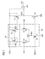
- Figure 1 shows an embodiment of such a comparator circuit known from the prior art. The problem with such a design is that when both input transistors are off or non conducting, the output of the comparator can be anything, this means is undefined.
- The comparator according to figure 1 has a first comparator input INP which is the non inverting input and a second comparator input INN which is the inverting input. Both comparator inputs INN and INP are connected to the control inputs of a difference amplifier transistor N1 and a difference amplifier transistor N2 of a difference amplifier DA. The difference amplifier DA further comprises a bias transistor N3 which is connected between an operating potential GND, also called ground, and the source connections of the difference amplifier transistors N1 and N2. The drain connections of the difference amplifier transistors N1 and N2 are connected to a current mirror CM comprising the current mirror transistors P1 and P2. The reference sign NET2 indicates the difference amplifier output which is placed between the drain of the difference amplifier transistor N2 and the source of the current mirror transistor P2. It leads to the control input of a transistor P3. The transistor P3 forms with a transistor N4 a serial connection which is connected between the operating potential GND and an operating potential VDD. At least an inverter INV1 is provided whose signal input is connected to the node NET4 placed between the two transistors P3 and N4 and whose power supply is the operating potential VDD. Its output forms the output OUT of the comparator. At the connector NBIAS connected to the control input of the bias transistor N3 a bias control voltage for controlling the bias current IBIAS flowing through the transistor N3 can be put. The connector NBIAS is also connected to the control input of the bias transistor N4.
- In figure 1 the reference signs *A, *B *C indicate how the transistor sizes should match, wherein the size of a transistor means its width and its length. For example the size of the transistors P1, P2 and P3 should match together and the width of transistor P3 should be twice the size of the transistor widths of the transistors P1 and P2. The transistors P1, P2 and P3 should also have the same length.
- The reference signs N1, N2, N3 and N4 mark the n-channel MOS or NMOS transistors while the reference signs P1, P2 and P3 mark the p-channel MOS or PMOS transistors.
- The comparator circuit works as follows. When the voltages at the comparator inputs INP and INN are the same and the difference amplifier transistors N1 and N2 are in saturated region, the current flowing in branch NET1 and the current flowing in branch NET2 are the equal. Furthermore, this currents are equal to the half of the bias current IBIAS. As a consequence of it, the voltage at NET2 is equal to the voltage at NET1 and the transistor P3 tries to force a current 2 * IBIAS / 2 = IBIAS in the branch NET4. Similarly, the bias transistor N4 tries to force a bias current IBIAS in the branch NET4. The voltage at node NET4 is between VDD and 0. This shows that transistors are sized ideally to minimize the systematic offset of the comparator.
- When the voltage at the non inverting comparator input INP is higher than the voltage at the inverting comparator input INN and at least one of the difference amplifier transistors N1 or N2 is on or conducting, the current flowing through the NET1 branch is greater than the current flowing through the NET2 branch. So when the current mirror constituted by the current mirror transistors P1 and P2 tries to force the current going in the NET1 branch on the NET2 branch, the voltage at node NET2 goes up. The current generated by the transistor P3 becomes lower than the current generated by the bias transistor N4 so the voltage at node NET4 goes down. The overall gain of the first and second stage is very high. Therefore, if the input voltage at the non inverting comparator input INP is only a little bit higher than the voltage at the inverting comparator input INN the voltage at node NET4 will be equal to 0. This leads that the voltage at the comparator output OUT will be equal to the operating potential VDD.
- When the voltage at the inverting comparator input INN is higher than the voltage at the non inverting comparator input INP and at least one of the difference amplifier transistors N1 or N2 is on or conducting, the current flowing through the NET2 branch is higher than the current flowing through the NET1 branch. So when the current mirror transistors P1 and P2 of the current mirror try to force the current going in NET1 branch on the NET2 branch, the voltage at node NET2 goes down. The current generated by the transistor P3 becomes higher than the current generated by the bias transistor N4 so the voltage at node NET4 goes up. Because the overall gain of the first and second stage is very high, it is sufficient that the input voltage at the inverting comparator input INN is only a little bit higher than the input voltage at the non inverting comparator input INP to have the voltage at node NET4 equal to the operating potential VDD. Therefore the voltage at the comparator output OUT will be 0.
- When both difference amplifier transistors N1 and N2 are switched off or non conducting because both input voltages at the comparators inputs INN and INP are low, the voltage at node NET2 is floating. Then the voltage at the comparator output OUT can be anything, this means is not defined.
- To solve this problem it is possible to use a rail to rail differential input stage for the comparator but this is increasing complexity and current consumption.
- An object of the invention is to provide a comparator which delivers a defined output signal when the input signals are low and simultaneously minimizes the complexity of the circuit.
- Another object of the invention is to provide a method for operating the comparator which delivers a defined output signal when the input signals are low.
- An advantage of the invention is that the current consumption stays low.
- The object of the invention is solved by a comparator with the features according to claim 1 and by a method for operating the comparator with the features according to the claim 8.
- The comparator according to the invention comprises a difference amplifier connected to a current mirror and a series connection of a first transistor and a second transistor connected between a first and a second operating potential, wherein the control input of the first transistor is connected to the difference amplifier and the current mirror. The comparator further comprises an inverter connected to the first operating potential and to the outputs of the first and second transistor. A third transistor is connected between the second operating potential and the output of the difference amplifier wherein the control input of the third transistor is connected to the output of the inverter.
- By the method for operating the comparator according to the invention the third transistor pulls the output of the difference amplifier to the second operating potential if the difference amplifier transistors are non conducting.
- Advantageous further developments of the invention arise from the characteristics indicated in the dependent patent claims.
- In an embodiment according to the invention the first transistor is a p-channel MOS-transistor.
- In a second embodiment according to the invention the second transistor is a n-channel MOS-transistor.
- In a third embodiment according to the invention the third transistor is a n-channel MOS-transistor.
- Advantageously in the comparator according to the invention the difference amplifier comprises a first difference amplifier transistor and a second difference amplifier transistor, wherein the control input of the first difference amplifier transistor is connected to a first comparator input, and wherein the control input of the second difference amplifier transistor is connected to a second comparator input.
- In another embodiment of the invention the control input of the second transistor is connected to a bias input. With that a bias current for the comparator can easily be adjusted.
- If the current mirror of the comparator according to the invention comprises n-channel transistors and the difference amplifier comprises p-channel transistors the control input of the second transistor can be connected to a bias input.
- Subsequently, the invention is further explained with the drawings.
- Figure 1
- shows an embodiment of a comparator according to the prior art.
- Figure 2
- shows an embodiment of a comparator according to the invention.
- Figure 3
- shows a modified version of the comparator according to figure 2.
- Figure 4
- shows a third embodiment of the comparator according to figure 2.
- Figure 5
- shows a modified version of the comparator according to figure 4.
- In the following a modification of the comparator according to figure 1 comprising a differential transistor pair with active loads is presented. By means of the modification the comparator output is set to a default value when both input transistors are switched off.
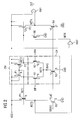
- The comparator according to figure 2 has as well as the comparator shown in figure 1 a first comparator input INP which is the non inverting input and a second comparator input INN which is the inverting input. Both comparator inputs INN and INP are connected to the control inputs of a difference amplifier transistor N1 and a difference amplifier transistor N2 of a difference amplifier DA. The difference amplifier DA further comprises a bias transistor N3 which is connected between an operating potential GND, also called ground, and the source connections of the difference amplifier transistors N1 and N2. The drain connections of the difference amplifier transistors N1 and N2 are connected to a current mirror CM comprising the current mirror transistors P1 and P2. The reference sign NET2 indicates the difference amplifier output. It leads to the control input of a transistor P3. The transistor P3 forms with a second bias transistor N4 a serial connection which is connected between the operating potential GND and the operating potential VDD. At least an inverter INV1 is provided whose signal input is connected to the two transistors P3 and N4 and whose power supply is the operating potential VDD. Its output forms the output OUT of the comparator. At the connector NBIAS connected to the control input of the bias transistor N3 a bias control voltage for controlling the bias current IBIAS flowing through the bias transistor N3 can be put. The connector NBIAS is also connected to the control input of the second bias transistor N4.
- In addition, the embodiment of the comparator shown in figure 2 comprises a series connection of a transistor P4 and a transistor N5 connected between the first and second operating potential VDD and GND, wherein the control input of the transistor P4 is connected to the drain of the difference amplifier transistor N1 of the difference amplifier DA and the source and gate of the current mirror transistor P1 of the current mirror CM. The comparator further comprises an inverter INV2 whose signal input is connected to the outputs of the two transistors P4 and N5 and whose power supply is the operating potential VDD. The outputs of a transistor N6 are connected between the operating potential GND and the output NET2 of the difference amplifier DA wherein the control input of the transistor N6 is connected to the output of the inverter INV2.
- In Figure 2 the reference signs *A, *B, *C show how the transistor sizes should match, wherein the size of a transistor means its width and its length. In the schematic according to Figure 2, the reference sign *C means that the sizes of the transistors N3, N4, N5 should match in the following way. The width of transistor N5 should be 0.4 times the width of the transistors N3 and N4, and the lengths of the transistors N3, N4, N5 should be the same. The matching values shown in Figure 2 are just given as an indication. There are many other matching values with which the invention will work correctly.
- The reference signs N1 to N6 mark the NMOS transistors while the reference signs P1 to P4 mark the PMOS transistors.
- Altogether, only five transistors namely P4, N5, N6 and two transistors for the inverter INV2 are added to the comparator shown in figure 1 to reach a defined comparator output signal when both difference amplifier transistors, also called input transistors, N1 and N2 are switched off.
- The comparator works as follows.
- The added circuit part of the comparator circuit is a redundant path when at least one of the difference amplifier transistors N1 and N2 is conducting.
- When the voltage at the non inverting comparator input INP is higher than the voltage at the inverting comparator input INN and at least one of the difference amplifier transistors N1 and N2 is conducting, the current in the branch NET1 will be higher than the half of the bias current IBIAS. The transistor P4 tries to mirror this current in the branch NET5 and the transistor N5 tries to force a current equal to 0.4 * IBIAS in it. This means that the voltage at node NET5 will be equal to the operating voltage VDD, the voltage at node NET6 will be 0 and the transistor N6 will be switched off. This means that the comparator will work as described in the prior art. A current flowing through the NET1 branch is higher than the current flowing through the NET2 branch. So when the current mirror CM constituted by the current mirror transistors P1 and P2 tries to force the current going in the NET1 branch on the NET2 branch, the voltage at node NET2 goes up to the operating potential VDD. When the voltage at the non inverting comparator input INP is higher than the voltage at the inverting comparator input INN and at least one of the difference amplifier transistors N1 and N2 is conducting, NET2 is forced to operating potential GND. Indeed, current flowing through the NET2 branch is higher than the current flowing through the NET1 branch. So when the current mirror transistors P1 and P2 of the current mirror try to force the current going in NET1 branch on the NET2 branch, the voltage at node NET2 goes down to operating potential GND. The circuitry added to the comparator of the prior art can either pull down the node NET2 to operating potential GND if the transistor N6 is conducting or can let it floating if the transistor N6 is not conducting. In both cases, it will not modify the comparator behavior.
- When the input voltage at the inverting comparator input INN is higher than the input voltage at the non inverting comparator input INP, the voltage at node NET2 is 0 for the standard comparator. So, the state of the transistor N6 will have no effect on node NET2 whatever its gate voltage is.
- But when the difference amplifier transistors N1 and N2 are switched off, the added circuitry changes the comparator behavior. Indeed, if no current is flowing through the branch NET1 the voltage at node NET5 is 0, the voltage at node NET6 is equal to the operating potential VDD, the voltage at node NET2 is 0, the voltage at node NET4 is equal to the operating voltage VDD and the voltage at the comparator output OUT is 0. This is the default value at the output OUT of the comparator circuit when both comparator inputs INN and INP are low.
- Figure 3 shows how to modify the comparator according to figure 2 in order to change the default comparator value when the input transistors are not conducting from 0 to VDD. A third inverter INV 3 is connected with its input to the output of the first inverter INV1. The output of the inverter INV3 forms now the output OUT of the comparator.
- Figure 4 shows a further modified embodiment of the comparator of figure 2 using PMOS input transistors instead of NMOS transistors. The default comparator value is VDD. The current mirror CM comprises in this embodiment two n-channel MOS transistors N1 and N2. The difference amplifier DA contains a first difference amplifier p-channel MOS transistor P1, a second difference amplifier p-channel MOS transistor P2 and a third p-channel MOS transistor P5, which is connected between the operating potential VDD and the first and second difference amplifier transistors P1 and P2. The p-channel transistors P3 and P4 are connected with its gate to a bias control voltage PBIAS.
- Figure 5 shows how to modify the comparator according to figure 4 in order to change the default comparator value when the input transistors are not conducting from VDD to 0. In this embodiment the difference amplifier DA and the current mirror CM are formed in the same way as the difference amplifier DA and the current mirror CM in the embodiment of figure 4. Just the inputs INP and INN are mixed up. A third inverter INV 3 is connected with its input to the output of the first inverter INV1. The output of the inverter INV3 forms the output OUT of the comparator.
- The schematics shown in the figures 3 to 5 are embodiments of the invention.
- Having illustrated and described a preferred embodiment for a novel comparator circuit, it is noted that variations and modifications in the circuit can be made without departing from the spirit of the invention or the scope of the appended claims.
-
- VDD
- power supply voltage
- GND
- ground or operating potential
- OUT
- comparator output
- CM
- current mirror
- DA
- difference amplifier
- INP
- non inverting comparator input
- INN
- inverting comparator input
- NBIAS
- input for bias voltage
- INV1
- first inverter
- INV2
- second inverter
- P1
- first current mirror transistor
- P2
- second current mirror transistor
- P3
- PMOS transistor
- P4
- PMOS transistor
- P5
- PMOS transistor
- N1
- first difference amplifier transistor
- N2
- second difference amplifier transistor
- N3
- first bias transistor
- N4
- second bias transistor
- N5
- NMOS transistor
- N6
- NMOS transistor
- S
- source
- NET1-5
- branch/node
- *A, *B, *C
- transistor size
Claims (8)
- Comparator, comprising
a difference amplifier (DA), connected to a current mirror (CM) ,
a series connection of a first transistor (P4) and a second transistor (N5) connected between a first and a second operating potential (VDD, GND), wherein the control input of said first transistor (P4) is connected to said difference amplifier (DA) and said current mirror (CM),
an inverter (INV2) connected to said first operating potential (VDD) and to the outputs of said first and second transistor (P4, N5), and
a third transistor (N6) connected between said second operating potential (GND) and the output (NET2) of said difference amplifier (DA) and wherein the control input of said third transistor (N6) is connected to the output of said inverter (INV2). - Comparator according to claim 1,
wherein the first transistor (P4) is a p-channel MOS-transistor. - Comparator according to claim 1 or 2,
wherein the second transistor (N5) is a n-channel MOS-transistor. - Comparator according to any preceding claim,
wherein the third transistor (N6) is a n-channel MOS-transistor. - Comparator according to any preceding claim,
wherein the difference amplifier (DA) comprises a first difference amplifier transistor (N1; P1) and a second difference amplifier transistor (N2; P2),
wherein the control input of the first difference amplifier transistor (N1; P1) is connected to a first comparator input (INP), and
wherein the control input of the second difference amplifier transistor (N2; P2) is connected to a second comparator input (INN). - Comparator according to any preceding claim,
wherein the control input of the second transistor (N5) is connected to a bias input (NBIAS). - Comparator according to any of the claims 1 to 5,
wherein the control input of the first transistor (P4) is connected to a bias input (PBIAS). - Method for operating a comparator according to claim 5 or 6,
wherein when the first and second difference amplifier transistor (N1, N2) are non conducting, the third transistor (N6) pulls the output (NET2) of the difference amplifier (DA) to the second operating potential (GND).
Priority Applications (4)
| Application Number | Priority Date | Filing Date | Title |
|---|---|---|---|
| AT03001720T ATE373341T1 (en) | 2003-01-27 | 2003-01-27 | COMPARATOR CIRCUIT AND METHOD THEREOF |
| EP03001720A EP1443647B1 (en) | 2003-01-27 | 2003-01-27 | Comparator and method for operating the comparator |
| DE60316249T DE60316249T2 (en) | 2003-01-27 | 2003-01-27 | Comparator circuit and method thereto |
| PCT/EP2004/000583 WO2004068711A2 (en) | 2003-01-27 | 2004-01-23 | Comparator and method for operating the comparator |
Applications Claiming Priority (1)
| Application Number | Priority Date | Filing Date | Title |
|---|---|---|---|
| EP03001720A EP1443647B1 (en) | 2003-01-27 | 2003-01-27 | Comparator and method for operating the comparator |
Publications (2)
| Publication Number | Publication Date |
|---|---|
| EP1443647A1 true EP1443647A1 (en) | 2004-08-04 |
| EP1443647B1 EP1443647B1 (en) | 2007-09-12 |
Family
ID=32605245
Family Applications (1)
| Application Number | Title | Priority Date | Filing Date |
|---|---|---|---|
| EP03001720A Expired - Lifetime EP1443647B1 (en) | 2003-01-27 | 2003-01-27 | Comparator and method for operating the comparator |
Country Status (4)
| Country | Link |
|---|---|
| EP (1) | EP1443647B1 (en) |
| AT (1) | ATE373341T1 (en) |
| DE (1) | DE60316249T2 (en) |
| WO (1) | WO2004068711A2 (en) |
Citations (2)
| Publication number | Priority date | Publication date | Assignee | Title |
|---|---|---|---|---|
| EP0488394A2 (en) * | 1990-11-29 | 1992-06-03 | Kabushiki Kaisha Toshiba | Oscillation circuit |
| WO2000005814A1 (en) * | 1998-07-20 | 2000-02-03 | Koninklijke Philips Electronics N.V. | Differential comparator with stable switching threshold |
Family Cites Families (2)
| Publication number | Priority date | Publication date | Assignee | Title |
|---|---|---|---|---|
| JPS5775022A (en) * | 1980-10-29 | 1982-05-11 | Nec Corp | Comparator |
| US4394587A (en) * | 1981-05-27 | 1983-07-19 | Motorola, Inc. | CMOS Differential comparator with hysteresis |
-
2003
- 2003-01-27 AT AT03001720T patent/ATE373341T1/en not_active IP Right Cessation
- 2003-01-27 DE DE60316249T patent/DE60316249T2/en not_active Expired - Lifetime
- 2003-01-27 EP EP03001720A patent/EP1443647B1/en not_active Expired - Lifetime
-
2004
- 2004-01-23 WO PCT/EP2004/000583 patent/WO2004068711A2/en not_active Ceased
Patent Citations (2)
| Publication number | Priority date | Publication date | Assignee | Title |
|---|---|---|---|---|
| EP0488394A2 (en) * | 1990-11-29 | 1992-06-03 | Kabushiki Kaisha Toshiba | Oscillation circuit |
| WO2000005814A1 (en) * | 1998-07-20 | 2000-02-03 | Koninklijke Philips Electronics N.V. | Differential comparator with stable switching threshold |
Also Published As
| Publication number | Publication date |
|---|---|
| EP1443647B1 (en) | 2007-09-12 |
| ATE373341T1 (en) | 2007-09-15 |
| WO2004068711A2 (en) | 2004-08-12 |
| WO2004068711A3 (en) | 2004-11-04 |
| DE60316249D1 (en) | 2007-10-25 |
| DE60316249T2 (en) | 2008-06-12 |
Similar Documents
| Publication | Publication Date | Title |
|---|---|---|
| KR100747328B1 (en) | Differential amplifier 0perable in wide range | |
| US7425844B1 (en) | Input buffer for multiple differential I/O standards | |
| JP3152867B2 (en) | Level shift semiconductor device | |
| CN101166026B (en) | Buffer circuit | |
| KR100355082B1 (en) | Operationally amplifying method and operational amplifier | |
| US6242980B1 (en) | Differential amplifier circuit | |
| JP4070533B2 (en) | Semiconductor integrated circuit device | |
| US6924702B2 (en) | Low supply voltage and self-biased high speed receiver | |
| JP2007116497A (en) | Operational amplifier | |
| US6930551B2 (en) | Zero voltage class AB minimal delay output stage and method | |
| US20080180173A1 (en) | Differential signal comparator | |
| US7005913B2 (en) | I/O buffer with wide range voltage translator | |
| KR20040076833A (en) | Semiconductor integrated circuit device | |
| JP4724670B2 (en) | Semiconductor integrated circuit device | |
| EP1443647B1 (en) | Comparator and method for operating the comparator | |
| KR100453424B1 (en) | Semiconductor integrated circuit | |
| US7532071B2 (en) | Operational amplifier circuit | |
| US20070024367A1 (en) | Operational amplifier and constant-current generation circuit using the same | |
| US7816989B2 (en) | Differential amplifier | |
| US6636109B2 (en) | Amplification circuit with constant output voltage range | |
| JP2809932B2 (en) | Input buffer circuit | |
| JP3385100B2 (en) | Operational amplifier | |
| US7564272B2 (en) | Differential amplifier | |
| JP3077664B2 (en) | Input circuit | |
| JP2002319855A (en) | Output signal control circuit for electronic equipment |
Legal Events
| Date | Code | Title | Description |
|---|---|---|---|
| PUAI | Public reference made under article 153(3) epc to a published international application that has entered the european phase |
Free format text: ORIGINAL CODE: 0009012 |
|
| AK | Designated contracting states |
Kind code of ref document: A1 Designated state(s): AT BE BG CH CY CZ DE DK EE ES FI FR GB GR HU IE IT LI LU MC NL PT SE SI SK TR |
|
| AX | Request for extension of the european patent |
Extension state: AL LT LV MK RO |
|
| 17P | Request for examination filed |
Effective date: 20050119 |
|
| AKX | Designation fees paid |
Designated state(s): AT DE FR GB |
|
| GRAP | Despatch of communication of intention to grant a patent |
Free format text: ORIGINAL CODE: EPIDOSNIGR1 |
|
| GRAS | Grant fee paid |
Free format text: ORIGINAL CODE: EPIDOSNIGR3 |
|
| GRAA | (expected) grant |
Free format text: ORIGINAL CODE: 0009210 |
|
| AK | Designated contracting states |
Kind code of ref document: B1 Designated state(s): AT DE FR GB |
|
| REG | Reference to a national code |
Ref country code: GB Ref legal event code: FG4D |
|
| REF | Corresponds to: |
Ref document number: 60316249 Country of ref document: DE Date of ref document: 20071025 Kind code of ref document: P |
|
| PG25 | Lapsed in a contracting state [announced via postgrant information from national office to epo] |
Ref country code: AT Free format text: LAPSE BECAUSE OF FAILURE TO SUBMIT A TRANSLATION OF THE DESCRIPTION OR TO PAY THE FEE WITHIN THE PRESCRIBED TIME-LIMIT Effective date: 20070912 |
|
| ET | Fr: translation filed | ||
| PLBE | No opposition filed within time limit |
Free format text: ORIGINAL CODE: 0009261 |
|
| STAA | Information on the status of an ep patent application or granted ep patent |
Free format text: STATUS: NO OPPOSITION FILED WITHIN TIME LIMIT |
|
| 26N | No opposition filed |
Effective date: 20080613 |
|
| GBPC | Gb: european patent ceased through non-payment of renewal fee |
Effective date: 20080127 |
|
| PG25 | Lapsed in a contracting state [announced via postgrant information from national office to epo] |
Ref country code: GB Free format text: LAPSE BECAUSE OF NON-PAYMENT OF DUE FEES Effective date: 20080127 |
|
| REG | Reference to a national code |
Ref country code: FR Ref legal event code: PLFP Year of fee payment: 14 |
|
| REG | Reference to a national code |
Ref country code: FR Ref legal event code: PLFP Year of fee payment: 15 |
|
| REG | Reference to a national code |
Ref country code: FR Ref legal event code: PLFP Year of fee payment: 16 |
|
| PGFP | Annual fee paid to national office [announced via postgrant information from national office to epo] |
Ref country code: FR Payment date: 20180119 Year of fee payment: 16 |
|
| PG25 | Lapsed in a contracting state [announced via postgrant information from national office to epo] |
Ref country code: FR Free format text: LAPSE BECAUSE OF NON-PAYMENT OF DUE FEES Effective date: 20190131 |
|
| PGFP | Annual fee paid to national office [announced via postgrant information from national office to epo] |
Ref country code: DE Payment date: 20210329 Year of fee payment: 19 |
|
| REG | Reference to a national code |
Ref country code: DE Ref legal event code: R119 Ref document number: 60316249 Country of ref document: DE |
|
| PG25 | Lapsed in a contracting state [announced via postgrant information from national office to epo] |
Ref country code: DE Free format text: LAPSE BECAUSE OF NON-PAYMENT OF DUE FEES Effective date: 20220802 |