EP1443552A2 - Semiconductor device and method of fabricating semiconductor device - Google Patents
Semiconductor device and method of fabricating semiconductor device Download PDFInfo
- Publication number
- EP1443552A2 EP1443552A2 EP03090434A EP03090434A EP1443552A2 EP 1443552 A2 EP1443552 A2 EP 1443552A2 EP 03090434 A EP03090434 A EP 03090434A EP 03090434 A EP03090434 A EP 03090434A EP 1443552 A2 EP1443552 A2 EP 1443552A2
- Authority
- EP
- European Patent Office
- Prior art keywords
- dummy patterns
- areas
- scribe line
- wafer
- arrangement
- Prior art date
- Legal status (The legal status is an assumption and is not a legal conclusion. Google has not performed a legal analysis and makes no representation as to the accuracy of the status listed.)
- Granted
Links
Images



Classifications
-
- H—ELECTRICITY
- H10—SEMICONDUCTOR DEVICES; ELECTRIC SOLID-STATE DEVICES NOT OTHERWISE PROVIDED FOR
- H10W—GENERIC PACKAGES, INTERCONNECTIONS, CONNECTORS OR OTHER CONSTRUCTIONAL DETAILS OF DEVICES COVERED BY CLASS H10
- H10W42/00—Arrangements for protection of devices
-
- H—ELECTRICITY
- H10—SEMICONDUCTOR DEVICES; ELECTRIC SOLID-STATE DEVICES NOT OTHERWISE PROVIDED FOR
- H10P—GENERIC PROCESSES OR APPARATUS FOR THE MANUFACTURE OR TREATMENT OF DEVICES COVERED BY CLASS H10
- H10P54/00—Cutting or separating of wafers, substrates or parts of devices
-
- H—ELECTRICITY
- H10—SEMICONDUCTOR DEVICES; ELECTRIC SOLID-STATE DEVICES NOT OTHERWISE PROVIDED FOR
- H10W—GENERIC PACKAGES, INTERCONNECTIONS, CONNECTORS OR OTHER CONSTRUCTIONAL DETAILS OF DEVICES COVERED BY CLASS H10
- H10W20/00—Interconnections in chips, wafers or substrates
- H10W20/01—Manufacture or treatment
- H10W20/031—Manufacture or treatment of conductive parts of the interconnections
- H10W20/062—Manufacture or treatment of conductive parts of the interconnections by smoothing of conductive parts, e.g. by planarisation
Definitions
- the invention relates to a semiconductor device and to a method of fabricating the device; and more particularly to a semiconductor device on which dummy patterns are formed on a wiring layer and to the method of fabricating the device.
- a method of fabricating a semiconductor device having a multiple interconnection layers when a method is adopted in which a wiring layer is formed by filling trenches with a metal, CMP (Chemical Mechanical Polishing) is used to remove unnecessary metal except the metal that has been embedded in the trenches. In such a case, a wiring pattern that has been formed unevenly on the wafer will cause variation in the polishing speed, and a countermeasure therefore is necessary for limiting variation in the film thickness of the wiring that is finally formed.
- a method has been conventionally adopted in which dummy patterns are arranged on the normal wiring layer.
- the dummy patterns referred to here are wiring patterns that are formed in scattered areas as a pseudo wiring pattern simultaneously with the wiring pattern, and moreover, by the same method as the wiring pattern.
- the easiest and most typical method of generating a dummy wiring pattern on data involves arranging uniform dummy patterns over the entire surface of pattern data and then removing the unnecessary dummy patterns based on a logical operation with the actual wiring pattern.
- This type of logical operation method is described in the specification of, for example, Japanese Patent No. 3128205.
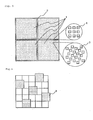
- FIG. 1 shows a plurality of chip areas 1 and scribe line areas 2 that demarcate each of chip areas 1 are provided on a wafer, and dummy patterns 3 and 4 are formed in areas 1 and 2, respectively.
- These dummy patterns are formed as square shapes, and the dummy patterns can be evenly generated in a grid composed of 5 by 5 squares as shown in FIG. 6 (to be described hereinbelow) by successively arranging these patterns in squares next to (in the example shown in FIG. 1 and FIG. 6, to the right of) squares that are two squares away in all directions: upward, downward, to the left and to the right of a particular dummy pattern.
- this arrangement of dummy patterns will be referred to as the "diagonally forward skipped arrangement".
- a film having a low dielectric constant itself has a low level of hardness, and further, has a low level of adhesion to the silicon oxide films or silicon nitride films that have been used conventionally as interlayer insulating films, and the use of a film having a low dielectric constant as the insulating film between wiring layers will therefore result in more extreme loss during dicing.
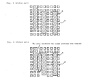
- the more concentrated arrangement of dummy patterns in a grid form results in dummy patterns that are arranged evenly with respect to the direction of the advance of the cutter and thus reduces the areas of loss. Nevertheless, the arrangement of dummy patterns in grid form over the entire surface of a wafer causes unevenness in the arrangement of the dummy patterns within the chip areas. This is because, in a construction in which wiring patterns of chip interior areas are arranged in one direction (vertical direction or horizontal direction) in all areas, as is normal, excessive separation will occur between areas in which the dummy patterns remain and areas in which the dummy patterns are removed as shown in FIG. 4 when the operation is performed for eliminating unnecessary patterns as described hereinabove (refer to FIGs. 2 - 4).
- a plurality of dummy patterns are formed in a grid arrangement in the scribe line areas of a wafer and a plurality of dummy patterns are formed in a diagonally forward skipped arrangement in the chip interior areas of the wafer.
- each of the dummy patterns that are formed in scribe-line areas may have a square shape or a rectangular shape, and each of the dummy patterns that are formed in areas within chips may have a square shape.
- FIG. 5 is a plan view showing
- a semiconductor device that uses a trench construction for forming wiring lines.
- scribe line areas 2 having a width of 100 ⁇ m are provided around the peripheries of chip areas 1 that have been formed on a silicon wafer.
- Dummy patterns 3 having a square shape measuring 2 ⁇ m on each side are arranged in the "diagonally forward skipped arrangement" in chip areas 1.
- dummy patterns 3 are arranged within grids that are repeated horizontally and vertically over the entire surface of chip areas 1, one grid being made up by 5 by 5 squares (a total of 25 squares) each square measuring 1.7 ⁇ m on a side arranged horizontally and vertically. In this arrangement, dummy patterns 3 are not uniformly arranged in the vertical direction, horizontal direction, and 45 degrees diagonal direction.
- dummy pattern 3 on the lower side coincides with the order of arrangement of dummy pattern 3 on the left side of one grid of 5 by 5 squares in the figure.
- dummy pattern 3 is arranged at the second square from the left on the lower side of the grid
- dummy pattern 3 is arranged at the second square from the top on the left side of the grid.
- a total of four dummy patterns 3 are provided at neighboring squares that are two squares over and one square to the right in all directions: upward, downward, to the right, and to the left; as seen from dummy pattern 3 that is arranged at the center of the one unit.
- a total of four dummy patterns 3 may also be provided at neighboring squares that are two squares over and one square to the left in all directions: upward, downward, to the left, and to the right; as seen from dummy pattern 3 that is arranged at the center of the one unit.
- each dummy pattern 3 is larger than one square in the present embodiment, the size of dummy patterns 3 can be varied as appropriate.
- the size of dummy patterns 3 is set in consideration of the density of wiring layout, and it is therefore possible, for example, for each dummy pattern 3 to be equal in size to each square, or for each dummy pattern 3 to be smaller than each square.
- FIGs. 7 to 9 show the method of designing the arrangement of dummy patterns in the present embodiment.
- Dummy patterns 3 can be automatically generated by using computer software that can execute the processes of: first employing a logical operation to avoid interference with the actual pattern and thus obtain the logical product of actual wiring pattern 5 and dummy pattern 3 (see FIG. 7); deleting dummy patterns 3 that overlap this actual wiring pattern 5 (see FIG. 8); and further deleting dummy patterns that do not attain a prescribed size (see FIG. 9).
- the wiring of an actual pattern is typically arranged parallel vertically or horizontally, and as a result, when the arrangement of the dummy pattern is for example a grid arrangement, the use of a logical operation as described hereinabove has the potential of generating areas in which there are no dummy patterns over areas that extend long distances vertically or horizontally.
- the arrangement of wiring patterns that include actual patterns and dummy patterns consequently becomes uneven, thereby preventing uniform CMP.
- dummy patterns are arranged in the "diagonally forward skipped arrangement"
- the direction of arrangement of the dummy patterns diverges from the direction of arrangement of the actual pattern, whereby even the above-described calculation method can leave uniform dummy patterns.
- square-shaped dummy patterns 4 measuring 2 ⁇ m on a side are arranged in a grid form with vertical and horizontal spacing of 2 ⁇ m in scribe line areas 2.
- the above-described logical operation is also applicable to scribe line areas 2 to remove dummy patterns 4 that interfere with actual patterns on scribe lines (for example, patterns for alignment of exposure masks or check patterns for checking products in the wafer state).
- the proportion of space of the entire wafer that is occupied by scribe line areas 2 is small, and the previously described effect is therefore small even when unevenness occurs in the wiring pattern.
- scribe line areas 2 of the wafer can be considered to be a substantially uniform material in the dicing process. Accordingly, loss (breaks in the wafer or film peeling) is suppressed during dicing of scribe line areas 2.
- a cutter for example, a rotary dicing blade.
- the width of the cutter used in this dicing process is 30 ⁇ m.
- cutting speed the rotational speed of the cutter is 36,000 rpm and the speed of movement of the stage is 3 mm/sec.
- the dummy patterns of scribe line areas 2 may be formed as, for example, rectangles each measuring 2 ⁇ m by 4 ⁇ m and arranged such that the longitudinal direction of these dummy patterns coincides with the direction of dicing (see reference numeral 6 in FIG. 10).
- FIG. 11 shows a semiconductor device which has a multi-layer wiring construction with improved resistance to loss in scribe line areas 2.
- the embodiment takes as example a semiconductor device having multilayer wiring that is made up of three wiring layers.
- the arrangement and dimensions of dummy patterns 7 and 8 in each wiring layer are similar to those of the first embodiment.
- FIG. 12 is a sectional view showing a section taken along line A-A in FIG. 11. Overlying and underlying dummy patterns 8 of each wiring layer in scribe line areas 2 are connected by via-holes 9. Via-holes 9 are formed simultaneously with and by the same method as the via-holes in actual patterns within the chips. Although only three wiring layers are shown in FIG. 12, additional insulating layers or wiring layers may of course be formed over these wiring layers in the finally formed semiconductor device.
- the use of via-holes 9 to connect dummy patterns 8 that overlie and underlie each wiring layer in scribe line areas 2 improves the adhesion between overlying and underlying dummy patterns 8, and moreover, increases the uniformity of hardness in scribe line areas 2.
- the embodiment can therefore suppress the expansion of areas of loss that occur during dicing due to the low level of adhesion between dummy pattern 8 of each layer and interlayer insulating films 11 - 16.
Landscapes
- Semiconductor Integrated Circuits (AREA)
- Internal Circuitry In Semiconductor Integrated Circuit Devices (AREA)
- Dicing (AREA)
- Design And Manufacture Of Integrated Circuits (AREA)
Abstract
Description
- The invention relates to a semiconductor device and to a method of fabricating the device; and more particularly to a semiconductor device on which dummy patterns are formed on a wiring layer and to the method of fabricating the device.
- In a conventional method of fabricating a semiconductor device having a multiple interconnection layers, when a method is adopted in which a wiring layer is formed by filling trenches with a metal, CMP (Chemical Mechanical Polishing) is used to remove unnecessary metal except the metal that has been embedded in the trenches. In such a case, a wiring pattern that has been formed unevenly on the wafer will cause variation in the polishing speed, and a countermeasure therefore is necessary for limiting variation in the film thickness of the wiring that is finally formed. For this purpose, a method has been conventionally adopted in which dummy patterns are arranged on the normal wiring layer. The dummy patterns referred to here are wiring patterns that are formed in scattered areas as a pseudo wiring pattern simultaneously with the wiring pattern, and moreover, by the same method as the wiring pattern.
- The easiest and most typical method of generating a dummy wiring pattern on data involves arranging uniform dummy patterns over the entire surface of pattern data and then removing the unnecessary dummy patterns based on a logical operation with the actual wiring pattern. This type of logical operation method is described in the specification of, for example, Japanese Patent No. 3128205.
- FIG. 1 shows
a plurality ofchip areas 1 and scribeline areas 2 that demarcate each ofchip areas 1 are provided on a wafer, anddummy patterns areas - When semiconductor devices are cut from a wafer to chip size by dicing, a process is carried out in which the wafer is cut by means of a diamond cutter. The occurrence of nonuniformity in the pattern that is formed on the cutting space of this cutter causes variation in the hardness of the wafer encountered by the cutter, and this variation tends to cause loss during cutting. In particular, when the pattern is scattered, the hardness is uniform in that portion, and loss that has once occurred tends to spread over a large area, resulting in an expanded area of loss. A construction having the "diagonally forward skipped arrangement" described hereinabove entails an increased probability that the arrangement of the dummy pattern will become sparse with respect to the direction of advance of the cutter and that a greater loss will thus occur.
- In addition, in the interest of improving the performance of semiconductor devices, recent years have seen the increased use of partial films having a low dielectric constant as the insulating film between wiring layers. Typically, a film having a low dielectric constant itself has a low level of hardness, and further, has a low level of adhesion to the silicon oxide films or silicon nitride films that have been used conventionally as interlayer insulating films, and the use of a film having a low dielectric constant as the insulating film between wiring layers will therefore result in more extreme loss during dicing.
- The more concentrated arrangement of dummy patterns in a grid form results in dummy patterns that are arranged evenly with respect to the direction of the advance of the cutter and thus reduces the areas of loss. Nevertheless, the arrangement of dummy patterns in grid form over the entire surface of a wafer causes unevenness in the arrangement of the dummy patterns within the chip areas. This is because, in a construction in which wiring patterns of chip interior areas are arranged in one direction (vertical direction or horizontal direction) in all areas, as is normal, excessive separation will occur between areas in which the dummy patterns remain and areas in which the dummy patterns are removed as shown in FIG. 4 when the operation is performed for eliminating unnecessary patterns as described hereinabove (refer to FIGs. 2 - 4).
- It is an object of the invention to provide a semiconductor device and a method of fabricating a semiconductor device in which dummy patterns are evenly formed in chip interior areas, and moreover, in which dummy patterns having superior resistance to loss when dicing are formed in scribe line areas.
- According to the invention, a plurality of dummy patterns are formed in a grid arrangement in the scribe line areas of a wafer and a plurality of dummy patterns are formed in a diagonally forward skipped arrangement in the chip interior areas of the wafer. This alteration of the dummy pattern arrangement enables the formation of dummy patterns with high uniformity in chip interior areas and enables the formation of dummy patterns with high resistance to the loss that occurs during dicing in scribe-line areas, thereby allowing an improvement in both the yield and the reliability of semiconductor chips that are obtained by cutting from a wafer.
- Further, each of the dummy patterns that are formed in scribe-line areas may have a square shape or a rectangular shape, and each of the dummy patterns that are formed in areas within chips may have a square shape.
- The above and other objects, features, and advantages of the invention will become apparent from the following description with reference to the accompanying drawings, which illustrate examples of the present invention.
-
- FIG. 1 is a plan view showing the arrangement of dummy patterns of the prior art;
- FIG. 2 is a plan view showing the first stage of the process of generating dummy patterns in a grid arrangement;
- FIG. 3 is a plan view showing the second stage of the process of generating dummy patterns in a grid arrangement;
- FIG. 4 is a plan view showing the third stage of the process of generating dummy patterns in a grid arrangement;
- FIG. 5 is a plan view showing a semiconductor device according to the first embodiment of the invention;
- FIG. 6 is a plan view showing the diagonally forward skipped arrangement of dummy patterns;
- FIG. 7 is a plan view showing the first stage of the process of generating dummy patterns in the diagonally forward skipped arrangement;
- FIG. 8 is a plan view showing the second stage of the process of generating dummy patterns in the diagonally forward skipped arrangement;
- FIG. 9 is a plan view showing the third stage of the process of generating dummy patterns in the diagonally forward skipped arrangement;
- FIG. 10 is a plan view showing another shape of a dummy pattern on a scribe line;
- FIG. 11 is a plan view showing a semiconductor device according to the second embodiment of the invention; and
- FIG. 12 is a sectional view showing dummy patterns on a scribe line in the second embodiment of the invention.
-
- FIG. 5 is a plan view showing,
- in particular, a semiconductor device that uses a trench construction for forming wiring lines.
- Referring to FIG. 5, scribe
line areas 2 having a width of 100 µm are provided around the peripheries ofchip areas 1 that have been formed on a silicon wafer.Dummy patterns 3 having a square shape measuring 2 µm on each side are arranged in the "diagonally forward skipped arrangement" inchip areas 1. - More specifically, as shown in FIG. 6,
dummy patterns 3 are arranged within grids that are repeated horizontally and vertically over the entire surface ofchip areas 1, one grid being made up by 5 by 5 squares (a total of 25 squares) each square measuring 1.7 µm on a side arranged horizontally and vertically. In this arrangement,dummy patterns 3 are not uniformly arranged in the vertical direction, horizontal direction, and 45 degrees diagonal direction. - The order of arrangement of
dummy pattern 3 on the lower side coincides with the order of arrangement ofdummy pattern 3 on the left side of one grid of 5 by 5 squares in the figure. In other words,dummy pattern 3 is arranged at the second square from the left on the lower side of the grid, anddummy pattern 3 is arranged at the second square from the top on the left side of the grid. In the present embodiment, moreover, in one unit of 5 by 5 squares, a total of fourdummy patterns 3 are provided at neighboring squares that are two squares over and one square to the right in all directions: upward, downward, to the right, and to the left; as seen fromdummy pattern 3 that is arranged at the center of the one unit. Alternatively, in one unit, a total of fourdummy patterns 3 may also be provided at neighboring squares that are two squares over and one square to the left in all directions: upward, downward, to the left, and to the right; as seen fromdummy pattern 3 that is arranged at the center of the one unit. - In addition, although each
dummy pattern 3 is larger than one square in the present embodiment, the size ofdummy patterns 3 can be varied as appropriate. The size ofdummy patterns 3 is set in consideration of the density of wiring layout, and it is therefore possible, for example, for eachdummy pattern 3 to be equal in size to each square, or for eachdummy pattern 3 to be smaller than each square. - FIGs. 7 to 9 show the method of designing the arrangement of dummy patterns in the present embodiment.
-
Dummy patterns 3 can be automatically generated by using computer software that can execute the processes of: first employing a logical operation to avoid interference with the actual pattern and thus obtain the logical product ofactual wiring pattern 5 and dummy pattern 3 (see FIG. 7); deletingdummy patterns 3 that overlap this actual wiring pattern 5 (see FIG. 8); and further deleting dummy patterns that do not attain a prescribed size (see FIG. 9). - The wiring of an actual pattern is typically arranged parallel vertically or horizontally, and as a result, when the arrangement of the dummy pattern is for example a grid arrangement, the use of a logical operation as described hereinabove has the potential of generating areas in which there are no dummy patterns over areas that extend long distances vertically or horizontally. The arrangement of wiring patterns that include actual patterns and dummy patterns consequently becomes uneven, thereby preventing uniform CMP. On the other hand, when dummy patterns are arranged in the "diagonally forward skipped arrangement", the direction of arrangement of the dummy patterns diverges from the direction of arrangement of the actual pattern, whereby even the above-described calculation method can leave uniform dummy patterns.
- Referring again to FIG. 5, square-
shaped dummy patterns 4 measuring 2 µm on a side are arranged in a grid form with vertical and horizontal spacing of 2 µm inscribe line areas 2. The above-described logical operation is also applicable to scribeline areas 2 to removedummy patterns 4 that interfere with actual patterns on scribe lines (for example, patterns for alignment of exposure masks or check patterns for checking products in the wafer state). The proportion of space of the entire wafer that is occupied byscribe line areas 2 is small, and the previously described effect is therefore small even when unevenness occurs in the wiring pattern. - Since
dummy patterns 4 are arranged in a grid pattern inscribe line areas 2,dummy patterns 4 and the spacing betweendummy patterns 4 are aligned evenly at a ratio of 1 : 1 in theseareas 2. As a result,scribe line areas 2 of the wafer can be considered to be a substantially uniform material in the dicing process. Accordingly, loss (breaks in the wafer or film peeling) is suppressed during dicing ofscribe line areas 2. During dicing, an area having a width of approximately 30 µm in the central portion ofscribe line areas 2 is cut by a cutter (for example, a rotary dicing blade). The width of the cutter used in this dicing process is 30 µm. As for cutting speed, the rotational speed of the cutter is 36,000 rpm and the speed of movement of the stage is 3 mm/sec. - Even should film peeling (in particular, peeling at the interface between the wiring metal and interlayer insulating film) occur in the dicing process, the interface in which peeling can occur is scattered with a constant narrow spacing that is equal to the pitch of
dummy patterns 4, and a film peeling that occurs at one location will not extend over a large area. - Further, as shown in FIG. 10, the dummy patterns of
scribe line areas 2 may be formed as, for example, rectangles each measuring 2 µm by 4 µm and arranged such that the longitudinal direction of these dummy patterns coincides with the direction of dicing (seereference numeral 6 in FIG. 10). - FIG. 11 shows a semiconductor device which has a multi-layer wiring construction with improved resistance to loss in
scribe line areas 2. The embodiment takes as example a semiconductor device having multilayer wiring that is made up of three wiring layers. The arrangement and dimensions ofdummy patterns 7 and 8 in each wiring layer are similar to those of the first embodiment. - FIG. 12 is a sectional view showing a section taken along line A-A in FIG. 11. Overlying and underlying dummy patterns 8 of each wiring layer in
scribe line areas 2 are connected by via-holes 9. Via-holes 9 are formed simultaneously with and by the same method as the via-holes in actual patterns within the chips. Although only three wiring layers are shown in FIG. 12, additional insulating layers or wiring layers may of course be formed over these wiring layers in the finally formed semiconductor device. - According to the present embodiment, the use of via-holes 9 to connect dummy patterns 8 that overlie and underlie each wiring layer in
scribe line areas 2 improves the adhesion between overlying and underlying dummy patterns 8, and moreover, increases the uniformity of hardness inscribe line areas 2. The embodiment can therefore suppress the expansion of areas of loss that occur during dicing due to the low level of adhesion between dummy pattern 8 of each layer and interlayer insulating films 11 - 16. - While preferred embodiments of the invention have been described using specific terms, such description is for illustrative purposes only, and it is to be understood that changes and variations may be made without departing from the spirit or scope of the following claims.
Claims (9)
- A semiconductor device, comprising:chip interior areas formed on a wafer that are provided with functional elements, and scribe line areas formed on said wafer that serve as cutting space when dicing said wafer;a plurality of dummy patterns arranged in a diagonally forward skipped arrangement that are formed in said chip interior areas; anda plurality of dummy patterns arranged in grid form that are formed in said scribe line areas.
- A semiconductor device according to claim 1, wherein:said semiconductor device includes a plurality of wiring layers that are stacked together, said dummy patterns being formed in said scribe line areas of each wiring layer; andsaid dummy patterns that are formed in said scribe line areas of each of said wiring layers are connected by via-holes.
- A method of fabricating a semiconductor device that includes chip interior areas formed on a wafer that are provided with functional elements, and scribe line areas formed on said wafer that serve as cutting space when dicing said wafer; said method comprising:a step of both forming a plurality of dummy patterns in a diagonally forward skipped arrangement in said chip interior areas and forming a plurality of dummy patterns in a grid arrangement in said scribe line areas.
- A method as claimed in claim 3, wherein each of said dummy patterns that are formed in said scribe line areas has a square shape or a rectangular shape.
- A method as claimed in claim 3 or 4,
wherein each of said dummy patterns that are formed in said chip interior areas has a square shape. - A method of fabricating a semiconductor device that includes chip interior areas formed on a wafer that are provided with functional elements, and scribe line areas formed on said wafer that serve as cutting space when dicing said wafer, and that further has a plurality of wiring layers that are stacked together, said method comprising;
a step of forming a plurality of dummy patterns in a diagonally forward skipped arrangement in said chip interior areas of each of said wiring layers and forming a plurality of dummy patterns in a grid arrangement in said scribe line areas of each of said wiring layers. - A method as claimed in claim 6, wherein each of said dummy patterns that are formed in said scribe line areas of each of said wiring layers has a square shape or a rectangular shape.
- A method as claimed in claim 6 or 7 ,
wherein each of said dummy patterns that are formed in said chip interior areas of each of said wiring layers has a square shape. - A method as claimed in any one of claims 6 to 8, further comprising:a step of connecting together said dummy patterns that are formed in said scribe line areas of each of said wiring layers by via-holes.
Applications Claiming Priority (2)
| Application Number | Priority Date | Filing Date | Title |
|---|---|---|---|
| JP2003021084 | 2003-01-29 | ||
| JP2003021084A JP4136684B2 (en) | 2003-01-29 | 2003-01-29 | Semiconductor device and dummy pattern arrangement method thereof |
Publications (3)
| Publication Number | Publication Date |
|---|---|
| EP1443552A2 true EP1443552A2 (en) | 2004-08-04 |
| EP1443552A3 EP1443552A3 (en) | 2005-04-20 |
| EP1443552B1 EP1443552B1 (en) | 2011-11-16 |
Family
ID=32652878
Family Applications (1)
| Application Number | Title | Priority Date | Filing Date |
|---|---|---|---|
| EP03090434A Expired - Lifetime EP1443552B1 (en) | 2003-01-29 | 2003-12-12 | Semiconductor device and method of fabricating semiconductor device |
Country Status (4)
| Country | Link |
|---|---|
| US (1) | US6841880B2 (en) |
| EP (1) | EP1443552B1 (en) |
| JP (1) | JP4136684B2 (en) |
| CN (1) | CN1316584C (en) |
Cited By (1)
| Publication number | Priority date | Publication date | Assignee | Title |
|---|---|---|---|---|
| US20080042155A1 (en) * | 2006-06-28 | 2008-02-21 | Oki Data Corporation | Semiconductor device, LED head and image forming apparatus |
Families Citing this family (55)
| Publication number | Priority date | Publication date | Assignee | Title |
|---|---|---|---|---|
| TWI222680B (en) * | 2003-11-20 | 2004-10-21 | United Microelectronics Corp | Scribe line structure of wafer |
| JP2005252099A (en) * | 2004-03-05 | 2005-09-15 | Sharp Corp | High frequency semiconductor devices |
| JP4471852B2 (en) * | 2005-01-21 | 2010-06-02 | パナソニック株式会社 | Semiconductor wafer, manufacturing method using the same, and semiconductor device |
| JP4455356B2 (en) * | 2005-01-28 | 2010-04-21 | Necエレクトロニクス株式会社 | Semiconductor device |
| JP4809632B2 (en) * | 2005-06-01 | 2011-11-09 | ルネサスエレクトロニクス株式会社 | Manufacturing method of semiconductor device |
| US7343581B2 (en) * | 2005-06-27 | 2008-03-11 | Tela Innovations, Inc. | Methods for creating primitive constructed standard cells |
| KR100794796B1 (en) * | 2005-09-08 | 2008-01-15 | 삼성전자주식회사 | Variable inductor |
| US7590968B1 (en) | 2006-03-01 | 2009-09-15 | Tela Innovations, Inc. | Methods for risk-informed chip layout generation |
| US8225239B2 (en) | 2006-03-09 | 2012-07-17 | Tela Innovations, Inc. | Methods for defining and utilizing sub-resolution features in linear topology |
| US9009641B2 (en) | 2006-03-09 | 2015-04-14 | Tela Innovations, Inc. | Circuits with linear finfet structures |
| US8658542B2 (en) | 2006-03-09 | 2014-02-25 | Tela Innovations, Inc. | Coarse grid design methods and structures |
| US8448102B2 (en) | 2006-03-09 | 2013-05-21 | Tela Innovations, Inc. | Optimizing layout of irregular structures in regular layout context |
| US8247846B2 (en) | 2006-03-09 | 2012-08-21 | Tela Innovations, Inc. | Oversized contacts and vias in semiconductor chip defined by linearly constrained topology |
| US7932545B2 (en) * | 2006-03-09 | 2011-04-26 | Tela Innovations, Inc. | Semiconductor device and associated layouts including gate electrode level region having arrangement of six linear conductive segments with side-to-side spacing less than 360 nanometers |
| US7446352B2 (en) | 2006-03-09 | 2008-11-04 | Tela Innovations, Inc. | Dynamic array architecture |
| US8839175B2 (en) | 2006-03-09 | 2014-09-16 | Tela Innovations, Inc. | Scalable meta-data objects |
| US7917879B2 (en) * | 2007-08-02 | 2011-03-29 | Tela Innovations, Inc. | Semiconductor device with dynamic array section |
| US8225261B2 (en) | 2006-03-09 | 2012-07-17 | Tela Innovations, Inc. | Methods for defining contact grid in dynamic array architecture |
| US8541879B2 (en) | 2007-12-13 | 2013-09-24 | Tela Innovations, Inc. | Super-self-aligned contacts and method for making the same |
| US9563733B2 (en) | 2009-05-06 | 2017-02-07 | Tela Innovations, Inc. | Cell circuit and layout with linear finfet structures |
| US8653857B2 (en) | 2006-03-09 | 2014-02-18 | Tela Innovations, Inc. | Circuitry and layouts for XOR and XNOR logic |
| US9230910B2 (en) | 2006-03-09 | 2016-01-05 | Tela Innovations, Inc. | Oversized contacts and vias in layout defined by linearly constrained topology |
| US7763534B2 (en) | 2007-10-26 | 2010-07-27 | Tela Innovations, Inc. | Methods, structures and designs for self-aligning local interconnects used in integrated circuits |
| US8245180B2 (en) | 2006-03-09 | 2012-08-14 | Tela Innovations, Inc. | Methods for defining and using co-optimized nanopatterns for integrated circuit design and apparatus implementing same |
| US7943967B2 (en) | 2006-03-09 | 2011-05-17 | Tela Innovations, Inc. | Semiconductor device and associated layouts including diffusion contact placement restriction based on relation to linear conductive segments |
| US9035359B2 (en) | 2006-03-09 | 2015-05-19 | Tela Innovations, Inc. | Semiconductor chip including region including linear-shaped conductive structures forming gate electrodes and having electrical connection areas arranged relative to inner region between transistors of different types and associated methods |
| US7956421B2 (en) | 2008-03-13 | 2011-06-07 | Tela Innovations, Inc. | Cross-coupled transistor layouts in restricted gate level layout architecture |
| US7586800B1 (en) | 2006-08-08 | 2009-09-08 | Tela Innovations, Inc. | Memory timing apparatus and associated methods |
| US7696607B2 (en) | 2006-08-10 | 2010-04-13 | Panasonic Corporation | Semiconductor device |
| DE102007004953A1 (en) * | 2007-01-26 | 2008-07-31 | Tesa Ag | heating element |
| US8286107B2 (en) | 2007-02-20 | 2012-10-09 | Tela Innovations, Inc. | Methods and systems for process compensation technique acceleration |
| US7979829B2 (en) * | 2007-02-20 | 2011-07-12 | Tela Innovations, Inc. | Integrated circuit cell library with cell-level process compensation technique (PCT) application and associated methods |
| US8667443B2 (en) | 2007-03-05 | 2014-03-04 | Tela Innovations, Inc. | Integrated circuit cell library for multiple patterning |
| US7799612B2 (en) * | 2007-06-25 | 2010-09-21 | Spansion Llc | Process applying die attach film to singulated die |
| KR20090046993A (en) | 2007-11-07 | 2009-05-12 | 주식회사 동부하이텍 | Semiconductor device and manufacturing method thereof |
| US8648444B2 (en) * | 2007-11-29 | 2014-02-11 | Taiwan Semiconductor Manufacturing Company, Ltd. | Wafer scribe line structure for improving IC reliability |
| US8453094B2 (en) | 2008-01-31 | 2013-05-28 | Tela Innovations, Inc. | Enforcement of semiconductor structure regularity for localized transistors and interconnect |
| US7939443B2 (en) | 2008-03-27 | 2011-05-10 | Tela Innovations, Inc. | Methods for multi-wire routing and apparatus implementing same |
| JP5309728B2 (en) * | 2008-06-27 | 2013-10-09 | 富士通セミコンダクター株式会社 | Reticle data creation method and reticle data creation device |
| KR101903975B1 (en) | 2008-07-16 | 2018-10-04 | 텔라 이노베이션스, 인코포레이티드 | Methods for cell phasing and placement in dynamic array architecture and implementation of the same |
| US9122832B2 (en) | 2008-08-01 | 2015-09-01 | Tela Innovations, Inc. | Methods for controlling microloading variation in semiconductor wafer layout and fabrication |
| US20100200957A1 (en) * | 2009-02-06 | 2010-08-12 | Qualcomm Incorporated | Scribe-Line Through Silicon Vias |
| JP5607317B2 (en) | 2009-06-17 | 2014-10-15 | ルネサスエレクトロニクス株式会社 | Semiconductor device manufacturing method and semiconductor wafer |
| JP5501668B2 (en) | 2009-06-17 | 2014-05-28 | ルネサスエレクトロニクス株式会社 | Semiconductor device manufacturing method, semiconductor chip, and semiconductor wafer |
| US8661392B2 (en) | 2009-10-13 | 2014-02-25 | Tela Innovations, Inc. | Methods for cell boundary encroachment and layouts implementing the Same |
| JP2011134893A (en) * | 2009-12-24 | 2011-07-07 | Renesas Electronics Corp | Semiconductor device |
| JP5468445B2 (en) | 2010-03-31 | 2014-04-09 | 株式会社東芝 | Semiconductor device and manufacturing method thereof |
| US8884402B2 (en) | 2010-04-28 | 2014-11-11 | United Microelectronics Corp. | Circuit layout structure |
| JP5516223B2 (en) * | 2010-08-19 | 2014-06-11 | 富士通株式会社 | Dummy metal arrangement evaluation apparatus, dummy metal arrangement evaluation method, and dummy metal arrangement evaluation program |
| US9159627B2 (en) | 2010-11-12 | 2015-10-13 | Tela Innovations, Inc. | Methods for linewidth modification and apparatus implementing the same |
| CN102445864A (en) * | 2011-10-21 | 2012-05-09 | 上海华力微电子有限公司 | Method for reducing photoetching alignment failure rate |
| CN103346129B (en) * | 2013-05-21 | 2016-07-06 | 北京新雷能科技股份有限公司 | A kind of ceramic package shell and preparation method thereof, chip packaging method |
| KR20150062556A (en) * | 2013-11-29 | 2015-06-08 | 삼성전기주식회사 | Strip level substrate having a member of preventing warpage and method of manufacturing the same |
| KR102633112B1 (en) | 2016-08-05 | 2024-02-06 | 삼성전자주식회사 | Semiconductor device |
| KR102698785B1 (en) | 2019-02-21 | 2024-08-27 | 삼성전자주식회사 | MIM capacitor and Semiconductor device |
Family Cites Families (8)
| Publication number | Priority date | Publication date | Assignee | Title |
|---|---|---|---|---|
| JP2000340568A (en) * | 1999-03-19 | 2000-12-08 | Toshiba Corp | Semiconductor device |
| JP2000286263A (en) | 1999-03-29 | 2000-10-13 | Nec Corp | Semiconductor device and manufacturing method thereof |
| JP2000340529A (en) * | 1999-05-31 | 2000-12-08 | Mitsubishi Electric Corp | Semiconductor device |
| US6528818B1 (en) * | 1999-12-14 | 2003-03-04 | Kla-Tencor | Test structures and methods for inspection of semiconductor integrated circuits |
| JP3551877B2 (en) * | 2000-01-18 | 2004-08-11 | セイコーエプソン株式会社 | Semiconductor device and manufacturing method thereof |
| JP2001332556A (en) * | 2000-05-25 | 2001-11-30 | Hitachi Ltd | Method for manufacturing semiconductor device |
| JP2002208676A (en) * | 2001-01-10 | 2002-07-26 | Mitsubishi Electric Corp | Semiconductor device, method of manufacturing semiconductor device, and method of designing semiconductor device |
| JP2003045876A (en) * | 2001-08-01 | 2003-02-14 | Seiko Epson Corp | Semiconductor device |
-
2003
- 2003-01-29 JP JP2003021084A patent/JP4136684B2/en not_active Expired - Lifetime
- 2003-11-19 US US10/715,503 patent/US6841880B2/en not_active Expired - Lifetime
- 2003-12-11 CN CNB200310120446XA patent/CN1316584C/en not_active Expired - Lifetime
- 2003-12-12 EP EP03090434A patent/EP1443552B1/en not_active Expired - Lifetime
Non-Patent Citations (1)
| Title |
|---|
| None |
Cited By (2)
| Publication number | Priority date | Publication date | Assignee | Title |
|---|---|---|---|---|
| US20080042155A1 (en) * | 2006-06-28 | 2008-02-21 | Oki Data Corporation | Semiconductor device, LED head and image forming apparatus |
| EP1873825A3 (en) * | 2006-06-28 | 2011-12-28 | Oki Data Corporation | Semiconductor device, LED head and image forming apparatus |
Also Published As
| Publication number | Publication date |
|---|---|
| EP1443552A3 (en) | 2005-04-20 |
| US6841880B2 (en) | 2005-01-11 |
| CN1316584C (en) | 2007-05-16 |
| US20040145028A1 (en) | 2004-07-29 |
| CN1519908A (en) | 2004-08-11 |
| JP4136684B2 (en) | 2008-08-20 |
| JP2004235357A (en) | 2004-08-19 |
| EP1443552B1 (en) | 2011-11-16 |
Similar Documents
| Publication | Publication Date | Title |
|---|---|---|
| US6841880B2 (en) | Semiconductor device and method of fabricating semiconductor device with high CMP uniformity and resistance to loss that occurs in dicing | |
| US11011471B2 (en) | Semiconductor device | |
| US7952167B2 (en) | Scribe line layout design | |
| US7087452B2 (en) | Edge arrangements for integrated circuit chips | |
| US7994613B2 (en) | Semiconductor device and method for manufacturing the same | |
| US10490514B2 (en) | Semiconductor devices | |
| JP4199846B2 (en) | Multilayer test pad on semiconductor wafer and method of forming the same | |
| CN102130049B (en) | Manufacturing method of semiconductor device and semiconductor device | |
| US20110156219A1 (en) | Semiconductor device | |
| US20060261490A1 (en) | Apparatus and method for manufacturing a semiconductor wafer with reduced delamination and peeling | |
| US6690045B2 (en) | Semiconductor device with reduced CMP dishing | |
| CN113937065B (en) | Semiconductor structure and method for manufacturing the same | |
| US7314811B2 (en) | Method to make corner cross-grid structures in copper metallization | |
| US20080142927A1 (en) | Scribe-line structures and methods of forming the same | |
| CN101315871A (en) | Method for manufacturing wafer and multi-project wafer | |
| KR20240033593A (en) | Method of manufacturing semiconductor chip including forming dicing grooves and semiconductor device | |
| KR102894823B1 (en) | Structure and method for sealing silicon ICs | |
| CN102569209A (en) | Anti-cracking structure | |
| US7091621B1 (en) | Crack resistant scribe line monitor structure and method for making the same | |
| KR102877317B1 (en) | Semiconductor wafer and method for fabricating the same | |
| CN100466252C (en) | Semiconductor wafer and method for manufacturing the same | |
| JP2003051470A (en) | Semiconductor device manufacturing method, mask pattern design method, and program | |
| TWI921875B (en) | Systems and methods for mitigating crack meandering in semiconductor dicing | |
| CN101866895B (en) | Chip structure and forming method thereof | |
| CN121712324A (en) | Semiconductor device forming method and semiconductor device |
Legal Events
| Date | Code | Title | Description |
|---|---|---|---|
| PUAI | Public reference made under article 153(3) epc to a published international application that has entered the european phase |
Free format text: ORIGINAL CODE: 0009012 |
|
| AK | Designated contracting states |
Kind code of ref document: A2 Designated state(s): AT BE BG CH CY CZ DE DK EE ES FI FR GB GR HU IE IT LI LU MC NL PT RO SE SI SK TR |
|
| AX | Request for extension of the european patent |
Extension state: AL LT LV MK |
|
| PUAL | Search report despatched |
Free format text: ORIGINAL CODE: 0009013 |
|
| AK | Designated contracting states |
Kind code of ref document: A3 Designated state(s): AT BE BG CH CY CZ DE DK EE ES FI FR GB GR HU IE IT LI LU MC NL PT RO SE SI SK TR |
|
| AX | Request for extension of the european patent |
Extension state: AL LT LV MK |
|
| RIC1 | Information provided on ipc code assigned before grant |
Ipc: 7H 01L 21/768 B Ipc: 7H 01L 21/321 B Ipc: 7H 01L 21/78 A |
|
| 17P | Request for examination filed |
Effective date: 20050426 |
|
| AKX | Designation fees paid |
Designated state(s): DE |
|
| RAP1 | Party data changed (applicant data changed or rights of an application transferred) |
Owner name: RENESAS ELECTRONICS CORPORATION |
|
| RIC1 | Information provided on ipc code assigned before grant |
Ipc: H01L 21/78 20060101AFI20110127BHEP Ipc: H01L 21/768 20060101ALN20110127BHEP Ipc: H01L 23/58 20060101ALI20110127BHEP |
|
| GRAP | Despatch of communication of intention to grant a patent |
Free format text: ORIGINAL CODE: EPIDOSNIGR1 |
|
| GRAS | Grant fee paid |
Free format text: ORIGINAL CODE: EPIDOSNIGR3 |
|
| GRAA | (expected) grant |
Free format text: ORIGINAL CODE: 0009210 |
|
| AK | Designated contracting states |
Kind code of ref document: B1 Designated state(s): DE |
|
| REG | Reference to a national code |
Ref country code: DE Ref legal event code: R096 Ref document number: 60339119 Country of ref document: DE Effective date: 20120209 |
|
| PLBE | No opposition filed within time limit |
Free format text: ORIGINAL CODE: 0009261 |
|
| STAA | Information on the status of an ep patent application or granted ep patent |
Free format text: STATUS: NO OPPOSITION FILED WITHIN TIME LIMIT |
|
| 26N | No opposition filed |
Effective date: 20120817 |
|
| REG | Reference to a national code |
Ref country code: DE Ref legal event code: R097 Ref document number: 60339119 Country of ref document: DE Effective date: 20120817 |
|
| PGFP | Annual fee paid to national office [announced via postgrant information from national office to epo] |
Ref country code: DE Payment date: 20220527 Year of fee payment: 20 |
|
| REG | Reference to a national code |
Ref country code: DE Ref legal event code: R071 Ref document number: 60339119 Country of ref document: DE |