EP1443525B1 - Strahlenvorbehandelter stimulierbarer Leuchtstoffschirm - Google Patents
Strahlenvorbehandelter stimulierbarer Leuchtstoffschirm Download PDFInfo
- Publication number
- EP1443525B1 EP1443525B1 EP20030104831 EP03104831A EP1443525B1 EP 1443525 B1 EP1443525 B1 EP 1443525B1 EP 20030104831 EP20030104831 EP 20030104831 EP 03104831 A EP03104831 A EP 03104831A EP 1443525 B1 EP1443525 B1 EP 1443525B1
- Authority
- EP
- European Patent Office
- Prior art keywords
- radiation
- laser
- phosphor
- panel
- csbr
- Prior art date
- Legal status (The legal status is an assumption and is not a legal conclusion. Google has not performed a legal analysis and makes no representation as to the accuracy of the status listed.)
- Expired - Lifetime
Links
Images

Classifications
-
- G—PHYSICS
- G21—NUCLEAR PHYSICS; NUCLEAR ENGINEERING
- G21K—HANDLING OF PARTICLES OR IONISING RADIATION NOT OTHERWISE PROVIDED FOR; IRRADIATION DEVICES; GAMMA RAY OR X-RAY MICROSCOPES
- G21K4/00—Conversion screens for the conversion of the spatial distribution of X-rays or particle radiation into visible images, e.g. fluoroscopic screens
-
- C—CHEMISTRY; METALLURGY
- C09—DYES; PAINTS; POLISHES; NATURAL RESINS; ADHESIVES; COMPOSITIONS NOT OTHERWISE PROVIDED FOR; APPLICATIONS OF MATERIALS NOT OTHERWISE PROVIDED FOR
- C09K—MATERIALS FOR MISCELLANEOUS APPLICATIONS, NOT PROVIDED FOR ELSEWHERE
- C09K11/00—Luminescent materials, e.g. electroluminescent or chemiluminescent
- C09K11/08—Luminescent materials, e.g. electroluminescent or chemiluminescent containing inorganic luminescent materials
- C09K11/77—Luminescent materials, e.g. electroluminescent or chemiluminescent containing inorganic luminescent materials containing rare earth metals
- C09K11/7728—Luminescent materials, e.g. electroluminescent or chemiluminescent containing inorganic luminescent materials containing rare earth metals containing europium
- C09K11/7732—Halogenides
- C09K11/7733—Halogenides with alkali or alkaline earth metals
Definitions
- the present invention relates a method for preparing a Eu-doped CsBr-type stimulable or storage phosphor screen or panel having a homogeneously and increased speed or sensitivity, besides marking ability.
- a higher speed stands for detection of higher amounts of photons by the photomultiplier. Noise is directly related with the number of detected quanta and is proportional therewith.
- Speed of a plate or panel for computed radiography is determined by the number of emitted photons per dose unit, set free by photostimulation of energy, stored in the stimulable phosphors after exposure to X-rays.
- pretreatment at short ultraviolet wavelengths preferably applied in the wavelength range from 150 nm up to 300 nm as e.g. by means of mercury vapour lamp emission at 254 nm, during a few seconds only, at a high intensity, offers a valuable tool to the manufacturer in order to reach the objects of the present invention set forth hereinbefore.
- a method for producing a binderless Eu-doped CsBr-type storage phosphor screen comprising the steps of :
- a Eu-doped CsBr-type storage phosphor screen or panel thus provides ratios of ultraviolet luminescence intensities of at least 10/9 after having been exposed to radiation having a wavelength in the range from 150 to 400 nm, measured at same sites of the screen or panel, once without and once with pretreatment of said storage phosphor screen or panel with short-ultraviolet radiation in the range from 150 to 300 nm, with an energy of at least 10 mJ/mm 2 .
- such a storage phosphor screen or panel provides a ratio of at least 10/7, and even more preferred a ratio of at least 10/5.
- UV lasers Apart from an ultraviolet radiation source use is advantageously made from ultraviolet lasers.
- said ultraviolet lasers are a quadruplicated Nd:YAG laser at 266 nm - thereby making use of the fourth harmonic of said laser, normally exciting at 1064 nm - quadruplicated Nd:YLF and Nd:YVO lasers.
- Nd:YLF lasers made available by QUANTRONIX Corporation 41 Research Way East Setauket NY 11733, USA, are even suitable for use at differing wavelengths, namely at 209, 211, 262 and 263 nm.
- an Alexandrite laser emitting at 193 nm produced by LIGHT AGE, Inc., Two Riverview Drive Somerset, NJ 08873, USA, is advantageously used.
- UV luminescence (at 254 and 365 nm, after irradiation with 254 nm) on the contrary thus shows a decreasing efficiency, even up to 50 %!
- An optical exposure pretreatment in order to increase sensitivity or speed of Eu-doped CsBr-type storage phosphor panels has thus been realised by irradiation with radiation sources selected from the group consisting of a mercury vapour lamp (at 254 nm), a deuterium lamp, a xenon lamp and a krypton lamp (both providing selected emission lines in the desired short ultraviolet range between 200 nm and 300 nm), a quadruplicated Nd:YAg laser at 266 nm - making use of the fourth harmonic oscillation -, dye lasers having an ultraviolet emitting dye (such as e.g.
- excimer lasers e.g. those with a gas as F 2 , ArF (193 nm), KrF (248 nm), XeBr (282 nm) or XeCl (308 nm), and frequency-enhanced (doubled- or quadruplicated) diode lasers.
- a method for producing a binderless Eu-doped CsBr-type storage phosphor screen comprising the steps of :
- said phosphor precursors are selected from the group consisting of CsBr, EuX 2 , EuX 2 , EuOX and Cs x Eu y X x+ ⁇ y , wherein x/y > 0.3, wherein ⁇ ⁇ 2 and wherein X is a halide selected from the group consisting of Cl, Br and I and combinations thereof.
- X is a halide selected from the group consisting of Cl, Br and I and combinations thereof.
- the mixture of phosphor precursors set forth above, provided from one and the same or differing evaporation sources (or boats) is brought in a condition for vapour deposition and said mixture is deposited on a substrate by a method selected from the group consisting of physical vapour deposition, thermal vapour deposition, chemical vapour deposition, electron beam deposition, radio frequency deposition and pulsed laser deposition.
- a method selected from the group consisting of physical vapour deposition, thermal vapour deposition, chemical vapour deposition, electron beam deposition, radio frequency deposition and pulsed laser deposition.
- heat-resistant containers or crucibles also called “boats”
- those "boats" are composed of heat-resistant materials or are coated with an inner layer as heat-resistant stainless steel, titanium, tungsten carbide, and heat-resistant alloys.
- the deposition is provided on a substrate, serving as a support sheet as e.g. heat-resistant resins, glass or metals (as e.g. aluminum).
- a substrate serving as a support sheet as e.g. heat-resistant resins, glass or metals (as e.g. aluminum).
- said substrate is advantageously cooled.
- Vacuum deposition of a phosphor on such a substrate e.g. advantageously proceeds so that during said vacuum deposition step said substrate is kept at a temperature T, such that 50 °C ⁇ T ⁇ 300 °C and that said vacuum deposition proceeds in an Ar-atmosphere with an Ar-pressure of at most 3 Pa.
- on-line deposition on a support, carried on a cooled roller, passing the evaporation sources is advantageously applied.
- a homogeneous deposition of the phosphor on such a substrate preferably an aluminum sheet or layer, provided on a cylindrical drum or even passing said drum as a continously run support, whether or not passing repeatedly
- advantage is taken from the fact that the thickness of the phosphor layer is kept more constant, even in the vicinity of the borders thereof. At the borders of a supported substrate a lower thickness is often measured, due to a "shadow” effect, and because the vapour cloud gets drawn away due to temperature gradients (often related with lower temperatures at the borders).
- an ultraviolet irradiation pretreatment is thus advantageously applied in the manufacturing process, during or after one or more steps as, e.g., during or after vapourisation of the phosphor precursors (wherein the ultraviolet radiation source can even be mounted in the vapourisation apparatus), during the step between vapourisation and heat treatment, during heat treatment (providing presence of the ultraviolet source e.g. in the oven wherein heating proceeds).
- the exposure pretreatment method is applicable to Eu-doped CsBr-type storage phosphor plates, more preferably comprising CsBr:Eu phosphors showing lack for homogeneity in speed (sensitivity) over the surface of the plate or panel.
- speed is not only increased, but homogeneity is improved and even corrected in order to have an excellent speed level and equal speed distribution over the whole panel surface. So sites showing an inferior speed are "corrected in speed" by a higher short-UV pretreatment dose than sites showing a higher speed.
- a method is thus offered for producing a Eu-doped CsBr-type stimulable phosphor screen or panel having homogeneous speed distribution over its surface by radiation exposure treatment with energy from a radiation source emitting short ultraviolet radiation in the range from 150 to 300 nm to the said storage phosphor plate or panel originally having inhomogeneous speed distribution over its panel surface.
- a method comprising the step of compensating deviations from previously measured speed inhomogeneity point by point by scanning the panel with said radiation source by the step of emitting variable energy amounts in order to compensate for the said deviations.
- a method of producing a Eu-doped CsBr-type stimulable phosphor screen or panel is offered, said screen or panel having homogeneous speed distribution over its surface by radiation exposure treatment with energy from a radiation source emitting short ultraviolet radiation in the range from 150 to 300 nm to the said storage phosphor plate or panel, originally having inhomogeneous speed distribution over its panel surface by the step of integrally irradiating the screen or panel, after covering it, at least partially, with one or more filters having differing densities, absorbing radiation from a source emitting short ultraviolet radiation in the range from 150 to 300 nm at differing parts.
- a method according to the present invention is further offered, wherein said radiation exposure treatment is given locally as an inscription or identification mark.
- markings with a short-UV-laser in a storage phosphor screen or panel, and more preferably in Eu-doped CsBr-type storage phosphor panel is advantageously applied in order to make identification possible.
- the said radiation exposure treatment is given by means of laser, a mercury vapour lamp or a mask.
- a method is further offered of providing a storage phosphor panel with an identification mark or inscription by means of a laser, a mercury vapour lamp or a mask, wherein marking proceeds with a laser having a wavelength in the range from 150 to 300 nm.
- said identification mark or inscription is a readable text (with figures and characters) or a machine readable code.
- said identification mark or inscription is a bar code.
- said radiation exposure treatment is given locally before any other radiation exposure treatment.
- the vapour deposition technique of the Eu-doped CsBr-type phosphors as applied in the method of the present invention provides ability to make screens from binderless phosphors (having needles with dimensions EP-A 1 359 204, wherein said needles have an average cross-section diameter in the range from 1-30 ⁇ m and an average length in the range from 100 to 1000 ⁇ m), in favour of sharpness of the image obtained after stimulation of stored energy, captured by the needle-shaped (cylindrical, block-shaped or prismatic) phosphors after exposure to X-rays.
- binderless phosphors having needles with dimensions EP-A 1 359 204, wherein said needles have an average cross-section diameter in the range from 1-30 ⁇ m and an average length in the range from 100 to 1000 ⁇ m
- the method of the present invention is advantageously be applied to a storage phosphor screen, wherein said CsBr:Eu stimulable phosphor is available in an amorphous form such as in a powder form, in form of ground binderless needles (originating from those as described above) or as ground melts from said powders or needles.
- a Eu-doped CsBr-type phosphor layer By making a lacquer, based on such an amorphous phosphor, on one or more polymer binders and on one or more solvents; and coating said lacquer on a substrate, followed by drying that coated layer, a Eu-doped CsBr-type phosphor layer can also be obtained and the method of the present invention may also be applied thereupon while manufacturing such a screen, in that during or after at least one of the manufacturing steps a radiation exposure treatment is given with energy from radiation sources emitting short ultraviolet radiation in the range from 150 nm to 300 nm with an energy of at least 10 mJ/mm 2 .
- said radiation source is selected from the group consisting of a mercury vapour lamp (at 254 nm), a deuterium lamp, a xenon lamp, a krypton lamp, a quadruplicated - frequency enhanced - Nd:YAG, Nd:YLF, a Nd:YVO or an Alexandrite laser, a dye laser, an excimer laser and a frequency-doubled or quadruplicated diode laser.
- said radiation source is selected from the group of gas excimer lasers consisting of F 2 (157 nm), ArF (193 nm), KrF (248 nm), XeBr (282 nm) and XeCl (308 nm).
- So identification is another important application with respect to controll of the production as a function of the raw stock phosphor precursor materials used during manufacturing by the method of the present invention of the storage phosphor screens or panels.
- CsBr:Eu screens were made via thermal vapour deposition of CsBr and EuOBr. Therefor CsBr was mixed with EuOBr and placed in a container in a vacuum deposition chamber. The phosphor was deposited on a glass disk with a thickness of 1.5 mm and a diameter of 40 mm. The distance between the container and the substrate was 10 cm. During evaporation, the substrate was rotated at 12 r.p.m.. The container with starting materials was heated to a temperature of 750°C. Before the start of the evaporation, the chamber was evacuated to a pressure of 4.10 -5 mbar.
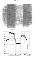
- Controlling under UV radiation (having a wavelength of 254 nm or 365 nm, as the experiments have been performed with the 254 nm line and the 365 nm line of a mercury vapour lamp - although radiation from the whole excitation spectrum in the range from 200 to 400 nm is not excluded and provides acceptable results) of the stimulable phosphor screen or panel thus obtained, led to the conclusion that a less intense UV luminescence signal was obtained at sites on the screen or panel, previously exposed to short-UV-rays with a radiation wavelength of 254 nm, obtained by a mercury lamp during 2 seconds or with the radiation wavelength of 266 nm obtained by a UV laser in the millisecond time range.
- Fig. 1B The corresponding sensitivity profiles for the different fields, measured as "SAL" have been illustrated in Fig. 1B.
- the sensitivities of those different fields or zones on the screen were measured in the following way: the screens were homogeneously exposed with a dose of ca. 50 mR at 80 kVp. Read-out was done in a flying spot scanner. In the scanner, the scanning light source was a 30 mW diode laser emitting at 685 nm. A 3-mm BG-39 ® (trade name of Schott) filter coated at both sides with a dielectrical layer was used in order to separate the stimulation light from the screen emission light. The scan-average levels (SAL's) were determined as the average signal produced by the screen fields in the photomultiplier tube.
- regions of the sheet or panel showing decreased ultraviolet luminescence after exposure to radiation having a wavelength of 254 nm show a sensitivity which is increased versus the non-exposed areas with about 35 % !
- Fig. 2A Inscriptions in form of a line with a UV laser having an exposure wavelength of 266 nm laser have been illustrated in Fig. 2A.
- the phosphor plate can be marked with an ultraviolet laser, e.g. at 266 nm, even without pre-exposure, but the effect described herein is not detectable on those sites that have been exposed to radiation at 254 nm anymore, as those sites are saturated.
- Fig. 2B shows the X-ray images obtained from the lines having been marked with a UV laser when the storage phosphor plate was pretreated with UV exposure having a wavelength of 254 nm: the storage plate or panel seems to be "saturated" as the laser exposure does not show a real inscription effect. Once saturated a laser inscription has reduced effect. It has been shown unambiguously that with a short-UV-pretreatment X-ray sensitivity or speed is enhanced. Once an increase up to 35 % (which is a very remarkable level) has been attained, saturation effects make that no further inscription is possible, thus putting a bar on it.
Landscapes
- Chemical & Material Sciences (AREA)
- Engineering & Computer Science (AREA)
- Physics & Mathematics (AREA)
- General Engineering & Computer Science (AREA)
- High Energy & Nuclear Physics (AREA)
- Inorganic Chemistry (AREA)
- Materials Engineering (AREA)
- Organic Chemistry (AREA)
- Conversion Of X-Rays Into Visible Images (AREA)
Claims (11)
- Ein durch die nachstehenden Schritte gekennzeichnetes Verfahren zur Herstellung einer bindemittelfreien Eu-dotierten CsBr-Speicherleuchtstofffolie :- Bereitstellen und Kombinieren von Leuchtstoffvorstufen zur Herstellung eines CsBr:Eu-Speicherleuchtstoffes,- Vakuumbeschichtung eines Substrats mit dem CsBr:Eu-Speicherleuchtstoff, wobei das Substrat während der Vakuumbeschichtung auf einer Temperatur zwischen 50°C und 300°C gehalten wird und die Vakuumbeschichtung in einer Argonatmosphäre bei einem Argondruck von höchstens 3 Pa erfolgt, dadurch gekennzeichnet, dass während oder nach zumindest einem der obigen Schritte eine Strahlungsbelichtungsbehandlung mit Energie von Strahlungsquellen, die kurzwellige Ultraviolettstrahlung mit einer Wellenlänge zwischen 150 nm und 300 nm mit einer Energie von zumindest 10 mJ/mm2 emittieren, vorgenommen wird.
- Verfahren nach Anspruch 1, dadurch gekennzeichnet, dass die Leuchtstoffvorstufen aus der Gruppe bestehend aus CsBr, EuX2, EuX2, EuOX und CsxEuyXx+αy gewählt werden, wobei x/y > 0,3, α ≥ 2 und X ein Halogenid aus der Gruppe bestehend aus Cl, Br und I und Kombinationen derselben ist.
- Verfahren nach Anspruch 1 oder 2, dadurch gekennzeichnet, dass die Strahlungsbelichtungsbehandlung darin besteht, dass Abweichungen einer im voraus gemessenen nicht-homogenen Empfindlichkeit punktweise durch Abtastung der Platte mit der Strahlungsquelle ausgeglichen werden, wobei die Strahlungsquelle variable Energiemengen zum Ausgleichen der Abweichungen emittiert.
- Verfahren nach Anspruch 1 oder 2, dadurch gekennzeichnet, dass die Strahlungsbelichtungsbehandlung besteht in der vollflächigen Bestrahlung der Folie oder Platte, die im voraus zumindest zum Teil mit einem oder mehreren Filtern mit unterschiedlichen Dichten, die von einer kurzwellige Ultraviolettstrahlung im Wellenlängenbereich zwischen 150 nm und 300 nm emittierenden Strahlungsquelle herrührende Strahlung absorbiert bzw. absorbieren, abgedeckt wird.
- Verfahren nach einem der Ansprüche 1 bis 4, dadurch gekennzeichnet, dass die Strahlungsbelichtungsbehandlung örtlich begrenzt in Form einer Beschriftungsmarkierung oder Identifikationsmarkierung erfolgt.
- Verfahren nach einem der Ansprüche 1 bis 5, dadurch gekennzeichnet, dass die Strahlungsbelichtungsbehandlung mittels eines Lasers, einer Quecksilberdampflampe, einer Deuteriumlampe, einer Xenonröhre, einer Kryptonlampe oder einer Maske erfolgt.
- Verfahren nach Anspruch 6, dadurch gekennzeichnet, dass als Laser ein frequenzvervierfachter - frequenzverbesserter - Nd:YAG-Laser, ein Nd:YFL-Laser, ein Nd:YVO-Laser oder ein Alexandrite-Laser, ein Farbstofflaser, ein Excimer-Laser oder ein frequenzverdoppelter oder frequenzvervierfachter Diodenlaser verwendet wird.
- Verfahren nach Anspruch 7, dadurch gekennzeichnet, dass als Excimer-Laser ein Gas-Excimer-Laser verwendet wird, wobei als Gas F2, ArF, KrF, XeBr oder XeCl verwendet wird.
- Verfahren nach einem der Ansprüche 5 bis 8, dadurch gekennzeichnet, dass die Identifikationsmarkierung oder Beschriftung ein lesbarer Text oder maschinenlesbarer Code ist.
- Verfahren nach einem der Ansprüche 5 bis 8, dadurch gekennzeichnet, dass die Identifikationsmarkierung oder Beschriftung ein Strichcode ist.
- Verfahren nach einem der Ansprüche 5 bis 10, dadurch gekennzeichnet, dass die Strahlungsbelichtungsbehandlung örtlich begrenzt vor jeglicher anderen Strahlungsbelichtungsbehandlung vorgenommen wird.
Priority Applications (1)
| Application Number | Priority Date | Filing Date | Title |
|---|---|---|---|
| EP20030104831 EP1443525B1 (de) | 2002-12-20 | 2003-12-19 | Strahlenvorbehandelter stimulierbarer Leuchtstoffschirm |
Applications Claiming Priority (3)
| Application Number | Priority Date | Filing Date | Title |
|---|---|---|---|
| EP02102863 | 2002-12-20 | ||
| EP02102863 | 2002-12-20 | ||
| EP20030104831 EP1443525B1 (de) | 2002-12-20 | 2003-12-19 | Strahlenvorbehandelter stimulierbarer Leuchtstoffschirm |
Publications (3)
| Publication Number | Publication Date |
|---|---|
| EP1443525A2 EP1443525A2 (de) | 2004-08-04 |
| EP1443525A3 EP1443525A3 (de) | 2004-08-18 |
| EP1443525B1 true EP1443525B1 (de) | 2006-12-06 |
Family
ID=32658184
Family Applications (1)
| Application Number | Title | Priority Date | Filing Date |
|---|---|---|---|
| EP20030104831 Expired - Lifetime EP1443525B1 (de) | 2002-12-20 | 2003-12-19 | Strahlenvorbehandelter stimulierbarer Leuchtstoffschirm |
Country Status (1)
| Country | Link |
|---|---|
| EP (1) | EP1443525B1 (de) |
Families Citing this family (2)
| Publication number | Priority date | Publication date | Assignee | Title |
|---|---|---|---|---|
| EP1892729A1 (de) * | 2006-08-10 | 2008-02-27 | Agfa HealthCare NV | Verfahren zur Herstellung eines Schirms zum Speichern eines Strahlungsbildes |
| US10125312B2 (en) * | 2016-09-06 | 2018-11-13 | Ut-Battelle, Llc | Divalent-ion-doped single crystal alkali halide scintillators |
Family Cites Families (2)
| Publication number | Priority date | Publication date | Assignee | Title |
|---|---|---|---|---|
| DE69214706T2 (de) * | 1991-04-26 | 1997-05-15 | Agfa Gevaert Nv | Lumineszenter Artikel mit Schutzüberzug und Herstellung |
| EP1113458B1 (de) * | 1999-12-27 | 2005-02-02 | Agfa-Gevaert | Binderfreier Speicherleuchtschirm mit nadelförmigen Kristallen und Verfahren zu dessen Erzeugung |
-
2003
- 2003-12-19 EP EP20030104831 patent/EP1443525B1/de not_active Expired - Lifetime
Also Published As
| Publication number | Publication date |
|---|---|
| EP1443525A3 (de) | 2004-08-18 |
| EP1443525A2 (de) | 2004-08-04 |
Similar Documents
| Publication | Publication Date | Title |
|---|---|---|
| US6875990B2 (en) | Radiation image storage panel | |
| US6899962B2 (en) | Europium activated cesium bromide phosphor and radiation image storage sheet | |
| US7141135B2 (en) | Manufacturing method of phosphor or scintillator sheets and panels suitable for use in a scanning apparatus | |
| EP1355322A2 (de) | Verfahren zur Herstellung eines Schirmes zum Speichern eines Strahlungsbildes mit Gasphasenabscheidungen | |
| US6707050B2 (en) | Radiation image storage panel | |
| JP2007039791A (ja) | リフレクタ、それを備えた加熱用るつぼおよび放射線像変換パネルの製造方法 | |
| EP1217633B1 (de) | Cesiumbromid-Speicherphosphor mit einem schmalen Emissionsspektrum durch UV-Anregung | |
| US7217944B2 (en) | Process and apparatus for producing evaporated phosphor sheets and an evaporated phosphor sheet produced by means of such process and apparatus | |
| US20050103273A1 (en) | Vacuum evaporation crucible and phosphor sheet manufacturing apparatus using the same | |
| EP1443525A2 (de) | Strahlenvorbehandelter stimulierbarer Leuchstoffschirm | |
| US7126135B2 (en) | Radiation pretreated stimulable phosphor screen or panel | |
| US20080035857A1 (en) | Method of manufacturing a radiation image storage panel | |
| US6894290B2 (en) | Radiation image storage panel | |
| EP1453064A1 (de) | Strahlenvorbehandelter stimulierbarer Leuchtstoffschirm | |
| US20060060792A1 (en) | Radiographic image conversion panel and method of manufacturing the same | |
| EP1460643A1 (de) | Herststellungsverfahren für Phosphor- oder Szintillatorfolien und Platten geeignet für eine Abtastvorrichtung | |
| US7439523B2 (en) | Method for preparing radiation image storage panel | |
| JP2006113007A (ja) | 放射線画像変換パネル | |
| EP1526553B1 (de) | Strahlungsbildwandler | |
| US7141805B2 (en) | Radiation image storage panel | |
| US6623661B2 (en) | Method for producing photostimulable phosphor | |
| EP1892729A1 (de) | Verfahren zur Herstellung eines Schirms zum Speichern eines Strahlungsbildes | |
| JP2005091146A (ja) | 放射線像変換パネル及び放射線像変換パネルの製造方法 | |
| JP2006177702A (ja) | 放射線画像変換パネルの製造装置及び放射線画像変換パネルの製造方法 | |
| JP2003279697A (ja) | 放射線像変換パネル |
Legal Events
| Date | Code | Title | Description |
|---|---|---|---|
| PUAI | Public reference made under article 153(3) epc to a published international application that has entered the european phase |
Free format text: ORIGINAL CODE: 0009012 |
|
| PUAL | Search report despatched |
Free format text: ORIGINAL CODE: 0009013 |
|
| AK | Designated contracting states |
Kind code of ref document: A2 Designated state(s): AT BE BG CH CY CZ DE DK EE ES FI FR GB GR HU IE IT LI LU MC NL PT RO SE SI SK TR |
|
| AX | Request for extension of the european patent |
Extension state: AL LT LV MK |
|
| AK | Designated contracting states |
Kind code of ref document: A3 Designated state(s): AT BE BG CH CY CZ DE DK EE ES FI FR GB GR HU IE IT LI LU MC NL PT RO SE SI SK TR |
|
| AX | Request for extension of the european patent |
Extension state: AL LT LV MK |
|
| RIC1 | Information provided on ipc code assigned before grant |
Ipc: 7C 09K 11/465 B Ipc: 7G 21K 4/00 A |
|
| 17P | Request for examination filed |
Effective date: 20050218 |
|
| AKX | Designation fees paid |
Designated state(s): DE FR GB |
|
| RBV | Designated contracting states (corrected) |
Designated state(s): DE FR GB |
|
| GRAP | Despatch of communication of intention to grant a patent |
Free format text: ORIGINAL CODE: EPIDOSNIGR1 |
|
| GRAS | Grant fee paid |
Free format text: ORIGINAL CODE: EPIDOSNIGR3 |
|
| GRAA | (expected) grant |
Free format text: ORIGINAL CODE: 0009210 |
|
| AK | Designated contracting states |
Kind code of ref document: B1 Designated state(s): DE FR GB |
|
| REG | Reference to a national code |
Ref country code: GB Ref legal event code: FG4D |
|
| RIC1 | Information provided on ipc code assigned before grant |
Ipc: C09K 11/77 20060101ALI20061030BHEP Ipc: G21K 4/00 20060101AFI20061030BHEP |
|
| REF | Corresponds to: |
Ref document number: 60310189 Country of ref document: DE Date of ref document: 20070118 Kind code of ref document: P |
|
| REG | Reference to a national code |
Ref country code: GB Ref legal event code: 732E |
|
| ET | Fr: translation filed | ||
| REG | Reference to a national code |
Ref country code: FR Ref legal event code: TP |
|
| PLBE | No opposition filed within time limit |
Free format text: ORIGINAL CODE: 0009261 |
|
| STAA | Information on the status of an ep patent application or granted ep patent |
Free format text: STATUS: NO OPPOSITION FILED WITHIN TIME LIMIT |
|
| 26N | No opposition filed |
Effective date: 20070907 |
|
| PGFP | Annual fee paid to national office [announced via postgrant information from national office to epo] |
Ref country code: FR Payment date: 20071129 Year of fee payment: 5 Ref country code: GB Payment date: 20071130 Year of fee payment: 5 |
|
| PGFP | Annual fee paid to national office [announced via postgrant information from national office to epo] |
Ref country code: DE Payment date: 20081211 Year of fee payment: 6 |
|
| GBPC | Gb: european patent ceased through non-payment of renewal fee |
Effective date: 20081219 |
|
| REG | Reference to a national code |
Ref country code: FR Ref legal event code: ST Effective date: 20090831 |
|
| PG25 | Lapsed in a contracting state [announced via postgrant information from national office to epo] |
Ref country code: GB Free format text: LAPSE BECAUSE OF NON-PAYMENT OF DUE FEES Effective date: 20081219 |
|
| PG25 | Lapsed in a contracting state [announced via postgrant information from national office to epo] |
Ref country code: FR Free format text: LAPSE BECAUSE OF NON-PAYMENT OF DUE FEES Effective date: 20081231 |
|
| PG25 | Lapsed in a contracting state [announced via postgrant information from national office to epo] |
Ref country code: DE Free format text: LAPSE BECAUSE OF NON-PAYMENT OF DUE FEES Effective date: 20100701 |