EP1440931A1 - Method for manufacturing metal microstructure - Google Patents
Method for manufacturing metal microstructure Download PDFInfo
- Publication number
- EP1440931A1 EP1440931A1 EP02777967A EP02777967A EP1440931A1 EP 1440931 A1 EP1440931 A1 EP 1440931A1 EP 02777967 A EP02777967 A EP 02777967A EP 02777967 A EP02777967 A EP 02777967A EP 1440931 A1 EP1440931 A1 EP 1440931A1
- Authority
- EP
- European Patent Office
- Prior art keywords
- resin mold
- photosensitive polymer
- ultraviolet radiation
- metal microstructure
- electron beam
- Prior art date
- Legal status (The legal status is an assumption and is not a legal conclusion. Google has not performed a legal analysis and makes no representation as to the accuracy of the status listed.)
- Withdrawn
Links
Images

Classifications
-
- B—PERFORMING OPERATIONS; TRANSPORTING
- B81—MICROSTRUCTURAL TECHNOLOGY
- B81C—PROCESSES OR APPARATUS SPECIALLY ADAPTED FOR THE MANUFACTURE OR TREATMENT OF MICROSTRUCTURAL DEVICES OR SYSTEMS
- B81C1/00—Manufacture or treatment of devices or systems in or on a substrate
-
- B—PERFORMING OPERATIONS; TRANSPORTING
- B81—MICROSTRUCTURAL TECHNOLOGY
- B81C—PROCESSES OR APPARATUS SPECIALLY ADAPTED FOR THE MANUFACTURE OR TREATMENT OF MICROSTRUCTURAL DEVICES OR SYSTEMS
- B81C99/00—Subject matter not provided for in other groups of this subclass
- B81C99/0075—Manufacture of substrate-free structures
- B81C99/0085—Manufacture of substrate-free structures using moulds and master templates, e.g. for hot-embossing
-
- C—CHEMISTRY; METALLURGY
- C25—ELECTROLYTIC OR ELECTROPHORETIC PROCESSES; APPARATUS THEREFOR
- C25D—PROCESSES FOR THE ELECTROLYTIC OR ELECTROPHORETIC PRODUCTION OF COATINGS; ELECTROFORMING; APPARATUS THEREFOR
- C25D1/00—Electroforming
- C25D1/003—3D structures, e.g. superposed patterned layers
-
- H—ELECTRICITY
- H05—ELECTRIC TECHNIQUES NOT OTHERWISE PROVIDED FOR
- H05K—PRINTED CIRCUITS; CASINGS OR CONSTRUCTIONAL DETAILS OF ELECTRIC APPARATUS; MANUFACTURE OF ASSEMBLAGES OF ELECTRICAL COMPONENTS
- H05K3/00—Apparatus or processes for manufacturing printed circuits
- H05K3/10—Apparatus or processes for manufacturing printed circuits in which conductive material is applied to the insulating support in such a manner as to form the desired conductive pattern
- H05K3/20—Apparatus or processes for manufacturing printed circuits in which conductive material is applied to the insulating support in such a manner as to form the desired conductive pattern by affixing prefabricated conductor pattern
- H05K3/205—Apparatus or processes for manufacturing printed circuits in which conductive material is applied to the insulating support in such a manner as to form the desired conductive pattern by affixing prefabricated conductor pattern using a pattern electroplated or electroformed on a metallic carrier
-
- H—ELECTRICITY
- H10—SEMICONDUCTOR DEVICES; ELECTRIC SOLID-STATE DEVICES NOT OTHERWISE PROVIDED FOR
- H10W—GENERIC PACKAGES, INTERCONNECTIONS, CONNECTORS OR OTHER CONSTRUCTIONAL DETAILS OF DEVICES COVERED BY CLASS H10
- H10W70/00—Package substrates; Interposers; Redistribution layers [RDL]
- H10W70/01—Manufacture or treatment
- H10W70/04—Manufacture or treatment of leadframes
-
- B—PERFORMING OPERATIONS; TRANSPORTING
- B81—MICROSTRUCTURAL TECHNOLOGY
- B81C—PROCESSES OR APPARATUS SPECIALLY ADAPTED FOR THE MANUFACTURE OR TREATMENT OF MICROSTRUCTURAL DEVICES OR SYSTEMS
- B81C2201/00—Manufacture or treatment of microstructural devices or systems
- B81C2201/03—Processes for manufacturing substrate-free structures
- B81C2201/032—LIGA process
-
- H—ELECTRICITY
- H05—ELECTRIC TECHNIQUES NOT OTHERWISE PROVIDED FOR
- H05K—PRINTED CIRCUITS; CASINGS OR CONSTRUCTIONAL DETAILS OF ELECTRIC APPARATUS; MANUFACTURE OF ASSEMBLAGES OF ELECTRICAL COMPONENTS
- H05K3/00—Apparatus or processes for manufacturing printed circuits
- H05K3/10—Apparatus or processes for manufacturing printed circuits in which conductive material is applied to the insulating support in such a manner as to form the desired conductive pattern
- H05K3/20—Apparatus or processes for manufacturing printed circuits in which conductive material is applied to the insulating support in such a manner as to form the desired conductive pattern by affixing prefabricated conductor pattern
- H05K3/202—Apparatus or processes for manufacturing printed circuits in which conductive material is applied to the insulating support in such a manner as to form the desired conductive pattern by affixing prefabricated conductor pattern using self-supporting metal foil pattern
Definitions
- the present invention relates to a method for manufacturing a metal microstructure used for a micromachine and the like.
- LIGA lithographie galvanoformung abformung
- SR synchrotron radiation
- the LIGA process is a processing technique combining lithography, plating such as electroforming, and molding.
- a resist film is formed on a conductive substrate, for example, and then is irradiated with SR ray through an absorbent mask having a pattern of predetermined shape to perform lithography.
- Such lithography allows a resist structure (resin mold) to be formed corresponding to the pattern shape of the absorbent mask.
- a vacant portion of the resist structure is then electroformed to obtain a metal microstructure.
- a high-precision metal microstructure obtained by further electroforming may be used as a mold to perform molding such as injection molding so as to obtain a micromolded article made of resin.
- Japanese Patent Laying-Open No. 2002-217461 discloses a method of manufacturing a metal microstructure as a mold by the LIGA process to form a micromolded article.
- lithography when lithography is used to form a metal microstructure, it can produce only one resist structure (resin mold) at a time. Therefore, lithography is not suitable for mass production. Furthermore, if a resin mold to be electroformed to form a metal microstructure is not fixed firmly with high precision onto a conductive substrate with an adhesive or the like, dimensional change or separation between the resin mold and the conductive substrate occurs in a subsequent step, disadvantageously resulting in a product of lower precision, a product not suitable for commercial use, and the like.
- An object of the present invention is to provide a method of manufacturing a metal microstructure by using a resin mold, in which a mild condition can be set so as to cause less damage to a resin mold and a high-precision metal microstructure can be mass-produced by uniform electroforming.
- a method of manufacturing a metal microstructure according to the present invention includes the steps of fixing on a conductive substrate a resin mold having a vacant portion penetrating in the direction of thickness, by interposing a photosensitive polymer having a chemical composition changed by one of the group consisting of an electron beam, ultraviolet radiation and visible radiation so as to form a layered structure having the resin mold; exposing the layered structure having the resin mold to the one of the group consisting of the electron beam, the ultraviolet radiation and the visible radiation; removing the exposed photosensitive polymer existing at the vacant portion of the resin mold; and filling with a metal the vacant portion of the layered structure having the resin mold by electroforming.
- the solvent having a lower ability to solve non-exposed photosensitive polymer and the resin mold's material than the exposed photosensitive polymer is preferably used.
- an etching gas whose etching rate is lower for the resin mold's material than for the exposed photosensitive polymer is preferably used.
- the resin mold fixed on the conductive substrate is of a type which blocks at least 95% of an electron beam, ultraviolet radiation or visible radiation by absorption or reflection.
- a resin mold having the bottom surface fixed on the conductive substrate and the top surface opposite thereto, one or both of the surfaces being covered with a material absorbing or reflecting an electron beam, ultraviolet radiation or visible radiation, a resin mold containing a material absorbing or reflecting an electron beam, ultraviolet radiation or visible radiation, or a resin mold having the top surface with irregularity and slanted to prevent an electron beam, ultraviolet radiation or visible radiation from being vertically incident is preferable.
- ultraviolet radiation having a wavelength of at most 300nm is preferably used.
- a method of manufacturing a metal microstructure according to the present invention includes the steps of: fixing a resin mold on a conductive substrate, by interposing a photosensitive polymer so as to form a layered structure having the resin mold; exposing; removing the exposed photosensitive polymer; and filling with a metal a vacant portion of the layered structure having the resin mold.
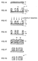
- Figs. 1A to 1G For the method of manufacturing a metal microstructure according to the present invention, an embodiment thereof will schematically be shown in Figs. 1A to 1G.
- a photosensitive polymer layer 12 having a thickness of several micrometers is formed on a conductive substrate 11 by spin coating, for example, as shown in Fig. 1A.
- a resin mold 13 having a vacant portion penetrating in the direction of thickness is then deposited.
- a layered structure 2 having the resin mold is formed.
- Photosensitive polymer layer 12 serves to bond and fix conductive substrate 11 and resin mold 13.
- the resin mold where a photosensitive polymer layer is formed on a conductive substrate and then a resin mold is fixed on the photosensitive polymer layer may be employed.
- a type having a chemical composition changed by an electron beam, ultraviolet radiation or visible radiation is used.
- a polymer which becomes easily removable by undergoing chemical change, such as change or decomposition of the functional group thereof, by an electron beam, ultraviolet radiation or visible radiation, being rendered easily soluble to a solvent, or the like is used.
- a photosensitive type is especially used because exposure causes chemical change which renders the polymer easily removable. As a result, a condition for the removal can be less severe, and accordingly, a resin mold can be less damaged by the removal.
- a photosensitive polymer which absorbs rays having a wavelength in the range of ultraviolet radiation (10nm-400nm of wavelength) or visible radiation, is used because ultraviolet radiation and visible radiation have more versatility and have smaller energy than X-ray, for example. Therefore, when such a ray of smaller energy is used as a light source for exposure, a resin mold can be less damaged.
- ultraviolet radiation having a wavelength of at most 300nm is preferable in that the efficiency of exposure thereof is easily improved.
- the ultraviolet radiation having a wavelength of at most 300nm can be obtained from an XeF lamp, or a typical mercury lamp in which a band-pass filter is inserted to block a ray having a wavelength of more than 300nm. By using these light sources, illuminance of several mW/cm 2 can be obtained depending on the light source's intensity.
- the photosensitive polymer used in the present invention has such photosensistivity.
- the photosensitive polymer has adhesion as described above and serves to fix the resin mold on the conductive substrate.
- such photosensitive polymer includes phenolic resin and novolak resin.
- the type mainly composed of quinone diazide compound is preferable in that it is rendered soluble to alkaline aqueous solution after exposure.
- the thickness of the photosensitive polymer layer is preferably 1-70 ⁇ m. If the thickness thereof is less than 1 ⁇ m, sufficient adhesive strength cannot be obtained. On the other hand, if the thickness thereof is more than 70 ⁇ m, it is difficult to obtain vertical cross section thereof. Therefore, the metal microstructure obtained later must be partially removed on the side of the conductive substrate by polishing or the like.
- Fig. 1A shows an example using conductive substrate 11.
- the thickness of the conductive substrate varies depending on its usage, ranging from only tens of micrometers to even no less than several millimeters. However, the thickness thereof is not limited thereto.
- Such conductive substrate 11 is formed of a material such as SUS, Al, Cu, and the like.
- a layered structure where a conductive layer is formed on a non-conductive substrate may also be used as a conductive substrate.
- a conductive layer made of Ti, Al, Cu, an alloy thereof, or the like, which is formed on a substrate made of Si, glass, ceramics, plastic, or the like, by vacuum evaporation, sputtering, plating, CVD, or the like, may be used.
- another type of thin metal film may be attached onto a conductive substrate if necessary.
- Resin mold 13 fixed on conductive substrate 11 by interposing photosensitive polymer layer 12 has a vacant portion penetrating in the direction of its thickness (Fig. 1B).
- the resin mold serves as an absorbent mask in the next step of exposure to an electron beam, ultraviolet radiation or visible radiation.
- the photosensitive polymer located at the bottom of the vacant portion is exposed while the photosensitive polymer located immediately below the resin mold is protected so that adhesion between the conductive substrate and the resin mold is assured.
- Such a resin mold is formed of a material such as polymethyl methacrylate, polypropylene, polycarbonate, and the like.
- the type which blocks in the next step of exposure at least 95% of an electron beam, ultraviolet radiation or visible radiation by absorption or reflection is preferable in that it effectively serves to protect the photosensitive polymer layer located immediately below the resin mold from the electron beam, ultraviolet radiation or visible radiation.
- a resin mold having the bottom surface fixed on the conductive substrate and the top surface opposite thereto, one or both of the surfaces being covered with a material absorbing or reflecting an electron beam, ultraviolet radiation or visible radiation, a resin mold containing a material absorbing or reflecting an electron beam, ultraviolet radiation or visible radiation, or a resin mold having the top surface slanted to prevent an electron beam, ultraviolet radiation or visible radiation from being vertically incident and having irregularity which tends to cause scattered reflection, is preferable.
- a resin mold formed by a combination of these types as such, as appropriate is effective, including a manner where absorption is weighed, a manner where reflection is weighed, and a manner where both absorption and reflection are weighed. Furthermore, these manners are also effective in the case where the resin mold is so thin that it does not sufficiently serve as an absorbent mask.
- the material forms a layer serving as a light exclusion layer to protect the photosensitive polymer immediately below the resin mold.
- the layer made of a material which absorbs or reflects an electron beam, ultraviolet radiation or visible radiation is provided on the top layer or the bottom layer, the layer provided at the bottom layer will serve more effectively. The shorter the distance between the photosensitive polymer layer and the layer made of a material which absorbs or reflects an electron beam, ultraviolet radiation or visible radiation, the larger effect of protecting the photosensitive polymer immediately below the resin mold can be obtained because wraparound by diffraction of an electron beam, ultraviolet radiation or visible radiation is decreased.
- a metal such as Al, Ti, Cu, Cr, Au, Ni and Ag, a metal compound such as Cr 2 O 3 and tungsten nitride (WN), or ceramics such as SiO 2 , Al 2 O 3 , SiC and AlN can be used.
- a metal compound such as Cr 2 O 3 and tungsten nitride (WN), or ceramics such as SiO 2 , Al 2 O 3 , SiC and AlN
- various types of methods including sputtering, vapor deposition, and the like; can be adopted.
- the resin mold containing a material absorbing or reflecting an electron beam, ultraviolet radiation or visible radiation is also preferable in that it effectively serves to block an electron beam, ultraviolet radiation or visible radiation and protect the photosensitive polymer immediately below the resin mold.
- the material absorbing or reflecting an electron beam ultraviolet radiation or visible radiation
- the metal, metal compound, or ceramics described above can be used.
- a colorant, an ultraviolet absorbent, or the like can also be used.
- the resin mold containing a material absorbing or reflecting an electron beam, ultraviolet radiation or visible radiation also includes a resin mold itself made of a material absorbing or reflecting an electron beam, ultraviolet radiation or visible radiation.
- ultraviolet radiation having a wavelength of at most 300nm is preferably used to perform exposure.
- SANRAD UXC-201 An example of the resin absorbing ultraviolet radiation having a wavelength of at most 300nm is SANRAD UXC-201 (made by Sanyo Chemical Industries, Ltd.).
- the resin mold made of SANRAD UXC-201 has high absorptance for ultraviolet radiation having a wavelength of at most 300nm, and if the thickness of the resin mold is reduced, at least 95% of ultraviolet radiation can easily be blocked. Therefore, ultraviolet radiation can easily be blocked and the thickness of the resin mold can also be reduced without covering the top surface or the bottom surface of the resin mold with an ultraviolet absorbent, providing irregularity to the top surface to obtain a rough surface, or adding an ultraviolet absorbent to the resin mold.
- the top surface of the resin mold has irregularity and is slanted to prevent an electron beam, ultraviolet radiation or visible radiation from being vertically incident.
- a larger quantity of light can be reflected and the photosensitive polymer immediately below the resin mold can be protected more effectively.
- the top surface's angle can be adjusted as appropriate in view of manufacturability.
- the top surface is made rough with irregularity, a quantity of the light passing through the resin mold can be reduced by scattered reflection to protect the photosensitive polymer immediately below the resin mold.
- Such a rough surface can be formed by sputtering, or alternatively, by mechanical processing with sandpaper, for example.
- the surface roughness (roughness of arithmetic mean Ra) of the top surface of the resin mold is preferably at least 1 ⁇ m.
- the layered structure having the resin mold is irradiated with an electron beam, ultraviolet radiation or visible radiation for 1-10 minutes for exposure. If the photosensitive polymer is applied on the conductive substrate and the resin mold is then attached thereon, a photosensitive polymer layer 12a exists at the bottom of the vacant portion of the layered structure 2 having the resin mold as shown in Fig. 1B. Alternatively, if the photosensitive polymer is applied to the bottom of the resin mold and then the resin mold is fixed on the conductive substrate (not shown), excessive photosensitive polymer overflows at the bottom of the vacant portion of the layered structure having the resin mold after the fixing step. In the step of exposing the layered structure having the resin mold, resin mold 13 itself serves as an absorbent mask as shown in Fig. 1C so that photosensitive polymer 12a at the bottom of the vacant portion of the layered structure having the resin mold is exposed to change into a polymer 12c having a chemical composition allowing easy removal by a solvent or by dry etching.
- the step of removing the exposed polymer can be performed by a solvent or by dry etching.
- Fig. 1D shows the state in which the exposed polymer at the bottom of the vacant portion of the resin mold is removed.
- a clean metal surface of the conductive substrate appears at the vacant portion of the layered structure having the resin mold.
- the vacant portion of the layered structure having the resin mold can be filled with a metal uniformly in the next step of electroforming so as to obtain a high-precision metal microstructure.
- a solvent liquid developer
- the ability to solve the resin mold's material is preferably at most 5% by weight, and more preferably, at most 3% by weight of the ability to solve the exposed polymer.
- a solvent (liquid developer) alkaline to a certain degree which does not affect the resin mold is preferably used. More particularly, if PMER P-LA100PM made by TOKYO OHKA CO., LTD. is used as a photosensitive polymer, PMER P-7G also made by TOKYO OHKA CO., LTD. is preferably used as an etching liquid.
- an etching gas whose etching rate is lower for the resin mold's material than for the exposed polymer is preferably used.
- the etching rate is a rate of removing a target by physical and chemical effects of an etching gas.
- a resin resistant to dry etching such as polyplopylene, polycyclic aromatic resin, or the like, is preferable. If phenolic resin or novolak resin of low molecular weight is used for the photosensitive polymer, Ar, SF 6 , O 2 , CF 4 , or a mixture thereof, for example, is preferable for an etching gas.
- the etching is preferably performed with RF power set to 10W-400W, and with the conductive substrate cooled to 0°C to -100°C. Ifthe conductive substrate is kept at high temperature, the resin mold and the non-exposed polymer immediately below the resin mold as well tend to suffer from erosion by lateral etching. If the conductive substrate is kept at low temperature ranging 0°C to -100°C, erosion of the non-exposed polymer immediately below the resin mold can be suppressed and selective etching only in the direction of a depth of the resin mold can be achieved. In the removing step, dry etching is superior to the use of a solvent described above in that dry etching involves a smaller number of steps and does not require a large number of washing steps, for example, because of its dryness.
- Electroforming is a process of forming a metal layer 14 on the conductive substrate by using a metal-ion solution. After forming metal layer 14, the metal layer is polished or ground to have a predetermined, uniform thickness.
- the metal microstructure obtained as such can be used for a circuit board, for example, with the conductive substrate placed thereon. Alternatively, the metal microstructure from which the conductive substrate is removed may also be used by itself
- the resin mold on the conductive substrate is removed by ashing using oxygen plasma, or the like. As a result, a structure shown in Fig. 1F can be obtained. By removing the conductive substrate from the structure, a metal microstructure 1 shown in Fig. 1G can be obtained.
- Metal microstructure 1 is a structure having a width of several micrometers to several hundreds of micrometers, a height of at most several hundreds of micrometers, and high aspect ratio. Furthermore, a sophisticated structure can be formed and the assembly work for the components is not required.
- the resin mold as mentioned above can be mass-replicated from a metal mold formed by the LIGA process, for example, and the resin mold can be electroformed to mass-produce the metal microstructure.
- Figs. 2A to 2D For a method of manufacturing the resin mold, an embodiment thereof is illustrated in Figs. 2A to 2D.
- Fig. 2A shows a metal mold having a convex portion 24.
- Such a metal mold is used to perform molding such as injection molding so as to form a resin mold 23 having a concave portion as shown in Fig. 2B.
- Fig. 2C shows resin mold 23 having a concave portion, from which the metal mold is removed.
- the resin mold is formed of a material such as polymethyl methacrylate, polypropylene, polycarbonate, or the like.
- the resin mold having a concave portion may also be formed by heat curing or photocuring.
- the resin mold is formed of a material such as acrylic resin, epoxy resin, or the like.
- resin mold 23 is polished, a resin mold 23a having a hole penetrating in the direction of a thickness as shown in Fig. 2D.
- the resin mold may be polished after it is bonded on the conductive substrate.
- a high-precision metal microstructure can be mass-produced under the mild manufacturing condition which causes less damage to the resin mold.
Landscapes
- Engineering & Computer Science (AREA)
- Chemical & Material Sciences (AREA)
- Manufacturing & Machinery (AREA)
- Microelectronics & Electronic Packaging (AREA)
- Crystallography & Structural Chemistry (AREA)
- Chemical Kinetics & Catalysis (AREA)
- Electrochemistry (AREA)
- Materials Engineering (AREA)
- Metallurgy (AREA)
- Organic Chemistry (AREA)
- Moulds For Moulding Plastics Or The Like (AREA)
- Micromachines (AREA)
Abstract
A method of manufacturing a metal microstructure (1) by using a resin mold
(13). In order to provide a method in which a mild manufacturing condition which
causes less damage to the resin mold (13) can be set and the high-precision metal
microstructure (1) can be mass-produced by uniform electroforming, the method of
manufacturing the metal microstructure (1) according to the present invention includes
the steps of: fixing on a conductive substrate (11) the resin mold (13) having a vacant
portion penetrating in the direction of thickness, by interposing a photosensitive polymer
(12) having a chemical composition changed by an electron beam, ultraviolet radiation
or visible radiation so as to form a layered structure (2) having the resin mold (13);
exposing the layered structure (2) having the resin mold (13) to an electron beam,
ultraviolet radiation or visible radiation; removing an exposed photosensitive polymer
(12c) existing at the vacant portion of the resin mold (13); and filling with a metal (14)
the vacant portion of the layered structure (2) having the resin mold (13) by
electroforming.
Description
The present invention relates to a method for manufacturing a metal
microstructure used for a micromachine and the like.
When a high-precision metal microstructure is mass-produced, a process of
lithographie galvanoformung abformung (LIGA) is useful. The LIGA process, which
uses synchrotron radiation (SR) ray among X-rays for its high directivity, is
characterized in that it allows deep lithography, processing of a structure having a height
of several hundreds of micrometers with a precision on the order of micrometers, easy
manufacturing of a metal microstructure having high aspect ratio, and the like.
Therefore, the LIGA process is expected to find application in various fields.
The LIGA process is a processing technique combining lithography, plating such
as electroforming, and molding. According to the LIGA process, a resist film is
formed on a conductive substrate, for example, and then is irradiated with SR ray
through an absorbent mask having a pattern of predetermined shape to perform
lithography. Such lithography allows a resist structure (resin mold) to be formed
corresponding to the pattern shape of the absorbent mask. A vacant portion of the
resist structure is then electroformed to obtain a metal microstructure. Furthermore, a
high-precision metal microstructure obtained by further electroforming may be used as a
mold to perform molding such as injection molding so as to obtain a micromolded article
made of resin. For example, Japanese Patent Laying-Open No. 2002-217461 discloses
a method of manufacturing a metal microstructure as a mold by the LIGA process to
form a micromolded article.
However, when lithography is used to form a metal microstructure, it can
produce only one resist structure (resin mold) at a time. Therefore, lithography is not
suitable for mass production. Furthermore, if a resin mold to be electroformed to form
a metal microstructure is not fixed firmly with high precision onto a conductive substrate
with an adhesive or the like, dimensional change or separation between the resin mold
and the conductive substrate occurs in a subsequent step, disadvantageously resulting in
a product of lower precision, a product not suitable for commercial use, and the like.
Furthermore, in the case where a typical adhesive is applied to the conductive substrate
to fix the resin mold thereon so as to solve the problem of a product of lower precision
and a defective product, if the adhesive remains at a vacant portion of the layered
structure having the resin mold, electromolding cannot be performed or insufficiently
performed thereon, disadvantageously resulting in an uneven metal layer formed thereby.
Furthermore, if the entire layered structure having the resin mold is etched to remove
the adhesive remaining at a vacant portion thereof, the resin mold itself is damaged
accordingly to a certain degree.
An object of the present invention is to provide a method of manufacturing a
metal microstructure by using a resin mold, in which a mild condition can be set so as to
cause less damage to a resin mold and a high-precision metal microstructure can be
mass-produced by uniform electroforming.
A method of manufacturing a metal microstructure according to the present
invention includes the steps of fixing on a conductive substrate a resin mold having a
vacant portion penetrating in the direction of thickness, by interposing a photosensitive
polymer having a chemical composition changed by one of the group consisting of an
electron beam, ultraviolet radiation and visible radiation so as to form a layered structure
having the resin mold; exposing the layered structure having the resin mold to the one of
the group consisting of the electron beam, the ultraviolet radiation and the visible
radiation; removing the exposed photosensitive polymer existing at the vacant portion of
the resin mold; and filling with a metal the vacant portion of the layered structure having
the resin mold by electroforming.
If the exposed photosensitive polymer is removed with a solvent, the solvent
having a lower ability to solve non-exposed photosensitive polymer and the resin mold's
material than the exposed photosensitive polymer is preferably used. Alternatively, if
the exposed photosensitive polymer is removed by dry etching, an etching gas whose
etching rate is lower for the resin mold's material than for the exposed photosensitive
polymer is preferably used.
Preferably, the resin mold fixed on the conductive substrate is of a type which
blocks at least 95% of an electron beam, ultraviolet radiation or visible radiation by
absorption or reflection. For such a resin mold, a resin mold having the bottom surface
fixed on the conductive substrate and the top surface opposite thereto, one or both of
the surfaces being covered with a material absorbing or reflecting an electron beam,
ultraviolet radiation or visible radiation, a resin mold containing a material absorbing or
reflecting an electron beam, ultraviolet radiation or visible radiation, or a resin mold
having the top surface with irregularity and slanted to prevent an electron beam,
ultraviolet radiation or visible radiation from being vertically incident is preferable. For
exposure, ultraviolet radiation having a wavelength of at most 300nm is preferably used.
A method of manufacturing a metal microstructure according to the present
invention includes the steps of: fixing a resin mold on a conductive substrate, by
interposing a photosensitive polymer so as to form a layered structure having the resin
mold; exposing; removing the exposed photosensitive polymer; and filling with a metal a
vacant portion of the layered structure having the resin mold.
For the method of manufacturing a metal microstructure according to the
present invention, an embodiment thereof will schematically be shown in Figs. 1A to 1G.
In the step of fixing a resin mold on a conductive substrate, by interposing a
photosensitive polymer so as to form a layered structure having the resin mold, a
photosensitive polymer layer 12 having a thickness of several micrometers is formed on
a conductive substrate 11 by spin coating, for example, as shown in Fig. 1A. As shown
in Fig. 1B, on photosensitive polymer layer 12, a resin mold 13 having a vacant portion
penetrating in the direction of thickness is then deposited. As a result, a layered
structure 2 having the resin mold is formed. Photosensitive polymer layer 12 serves to
bond and fix conductive substrate 11 and resin mold 13. By fixing conductive
substrate 11 and resin mold 13 firmly, lowering of precision caused by dimensional
change in a subsequent step and separation of resin mold 13 from conductive substrate
11 can be prevented. In addition to the resin mold where a photosensitive polymer
layer is formed on a conductive substrate and then a resin mold is fixed on the
photosensitive polymer layer, as described above, the resin mold where a photosensitive
polymer layer is formed on the bottom surface of a resin mold having a penetrating
vacant portion and then the resin mold is fixed on a conductive substrate (not shown)
may be employed.
For the photosensitive polymer, a type having a chemical composition changed
by an electron beam, ultraviolet radiation or visible radiation is used. In other words, a
polymer which becomes easily removable by undergoing chemical change, such as
change or decomposition of the functional group thereof, by an electron beam,
ultraviolet radiation or visible radiation, being rendered easily soluble to a solvent, or the
like, is used. In the present invention, a photosensitive type is especially used because
exposure causes chemical change which renders the polymer easily removable. As a
result, a condition for the removal can be less severe, and accordingly, a resin mold can
be less damaged by the removal. Similarly, a photosensitive polymer, which absorbs
rays having a wavelength in the range of ultraviolet radiation (10nm-400nm of
wavelength) or visible radiation, is used because ultraviolet radiation and visible
radiation have more versatility and have smaller energy than X-ray, for example.
Therefore, when such a ray of smaller energy is used as a light source for exposure, a
resin mold can be less damaged. Among these rays, ultraviolet radiation having a
wavelength of at most 300nm is preferable in that the efficiency of exposure thereof is
easily improved. The ultraviolet radiation having a wavelength of at most 300nm can
be obtained from an XeF lamp, or a typical mercury lamp in which a band-pass filter is
inserted to block a ray having a wavelength of more than 300nm. By using these light
sources, illuminance of several mW/cm2 can be obtained depending on the light source's
intensity.
The photosensitive polymer used in the present invention has such
photosensistivity. In addition, the photosensitive polymer has adhesion as described
above and serves to fix the resin mold on the conductive substrate. More specifically,
such photosensitive polymer includes phenolic resin and novolak resin. Of these resins,
the type mainly composed of quinone diazide compound is preferable in that it is
rendered soluble to alkaline aqueous solution after exposure. Furthermore, the
thickness of the photosensitive polymer layer is preferably 1-70µm. If the thickness
thereof is less than 1µm, sufficient adhesive strength cannot be obtained. On the other
hand, if the thickness thereof is more than 70µm, it is difficult to obtain vertical cross
section thereof. Therefore, the metal microstructure obtained later must be partially
removed on the side of the conductive substrate by polishing or the like.
Fig. 1A shows an example using conductive substrate 11. The thickness of the
conductive substrate varies depending on its usage, ranging from only tens of
micrometers to even no less than several millimeters. However, the thickness thereof is
not limited thereto. Such conductive substrate 11 is formed of a material such as SUS,
Al, Cu, and the like. Alternatively, a layered structure where a conductive layer is
formed on a non-conductive substrate (not shown) may also be used as a conductive
substrate. More particularly, a conductive layer made of Ti, Al, Cu, an alloy thereof,
or the like, which is formed on a substrate made of Si, glass, ceramics, plastic, or the
like, by vacuum evaporation, sputtering, plating, CVD, or the like, may be used.
Alternatively, another type of thin metal film may be attached onto a conductive
substrate if necessary.
For the resin mold, the type which blocks in the next step of exposure at least
95% of an electron beam, ultraviolet radiation or visible radiation by absorption or
reflection is preferable in that it effectively serves to protect the photosensitive polymer
layer located immediately below the resin mold from the electron beam, ultraviolet
radiation or visible radiation. By using such a resin mold, separation of the resin mold
from the substrate is prevented and a metal microstructure is easily formed in a stable
manner.
For such a resin mold, a resin mold having the bottom surface fixed on the
conductive substrate and the top surface opposite thereto, one or both of the surfaces
being covered with a material absorbing or reflecting an electron beam, ultraviolet
radiation or visible radiation, a resin mold containing a material absorbing or reflecting
an electron beam, ultraviolet radiation or visible radiation, or a resin mold having the top
surface slanted to prevent an electron beam, ultraviolet radiation or visible radiation
from being vertically incident and having irregularity which tends to cause scattered
reflection, is preferable. A resin mold formed by a combination of these types as such,
as appropriate is effective, including a manner where absorption is weighed, a manner
where reflection is weighed, and a manner where both absorption and reflection are
weighed. Furthermore, these manners are also effective in the case where the resin
mold is so thin that it does not sufficiently serve as an absorbent mask.
For the resin mold having one or both of the top and bottom surfaces covered
with a material absorbing or reflecting an electron beam, ultraviolet radiation or visible
radiation, the material forms a layer serving as a light exclusion layer to protect the
photosensitive polymer immediately below the resin mold. If the layer made of a
material which absorbs or reflects an electron beam, ultraviolet radiation or visible
radiation is provided on the top layer or the bottom layer, the layer provided at the
bottom layer will serve more effectively. The shorter the distance between the
photosensitive polymer layer and the layer made of a material which absorbs or reflects
an electron beam, ultraviolet radiation or visible radiation, the larger effect of protecting
the photosensitive polymer immediately below the resin mold can be obtained because
wraparound by diffraction of an electron beam, ultraviolet radiation or visible radiation
is decreased. For the material absorbing or reflecting an electron beam, ultraviolet
radiation or visible radiation, a metal such as Al, Ti, Cu, Cr, Au, Ni and Ag, a metal
compound such as Cr2O3 and tungsten nitride (WN), or ceramics such as SiO2, Al2O3,
SiC and AlN can be used. For the method of forming the light exclusion layer on the
top and bottom surfaces of the resin mold, various types of methods including sputtering,
vapor deposition, and the like; can be adopted.
The resin mold containing a material absorbing or reflecting an electron beam,
ultraviolet radiation or visible radiation is also preferable in that it effectively serves to
block an electron beam, ultraviolet radiation or visible radiation and protect the
photosensitive polymer immediately below the resin mold. For the material absorbing
or reflecting an electron beam, ultraviolet radiation or visible radiation, the metal, metal
compound, or ceramics described above can be used. Alternatively, a colorant, an
ultraviolet absorbent, or the like, can also be used. Furthermore, the resin mold
containing a material absorbing or reflecting an electron beam, ultraviolet radiation or
visible radiation also includes a resin mold itself made of a material absorbing or
reflecting an electron beam, ultraviolet radiation or visible radiation. As mentioned
above, ultraviolet radiation having a wavelength of at most 300nm is preferably used to
perform exposure. An example of the resin absorbing ultraviolet radiation having a
wavelength of at most 300nm is SANRAD UXC-201 (made by Sanyo Chemical
Industries, Ltd.). The resin mold made of SANRAD UXC-201 has high absorptance
for ultraviolet radiation having a wavelength of at most 300nm, and if the thickness of
the resin mold is reduced, at least 95% of ultraviolet radiation can easily be blocked.
Therefore, ultraviolet radiation can easily be blocked and the thickness of the resin mold
can also be reduced without covering the top surface or the bottom surface of the resin
mold with an ultraviolet absorbent, providing irregularity to the top surface to obtain a
rough surface, or adding an ultraviolet absorbent to the resin mold.
Preferably, the top surface of the resin mold has irregularity and is slanted to
prevent an electron beam, ultraviolet radiation or visible radiation from being vertically
incident. By slanting the top surface of the resin mold to prevent an electron beam,
ultraviolet radiation or visible radiation from being vertically incident, a larger quantity
of light can be reflected and the photosensitive polymer immediately below the resin
mold can be protected more effectively. As long as a larger quantity of light can be
reflected, the top surface's angle can be adjusted as appropriate in view of
manufacturability. Furthermore, if the top surface is made rough with irregularity, a
quantity of the light passing through the resin mold can be reduced by scattered
reflection to protect the photosensitive polymer immediately below the resin mold.
Such a rough surface can be formed by sputtering, or alternatively, by mechanical
processing with sandpaper, for example. In order to allow scattered reflection to
effectively decrease the quantity of light passing through, the surface roughness
(roughness of arithmetic mean Ra) of the top surface of the resin mold is preferably at
least 1µm.
In the step of exposure, the layered structure having the resin mold is irradiated
with an electron beam, ultraviolet radiation or visible radiation for 1-10 minutes for
exposure. If the photosensitive polymer is applied on the conductive substrate and the
resin mold is then attached thereon, a photosensitive polymer layer 12a exists at the
bottom of the vacant portion of the layered structure 2 having the resin mold as shown
in Fig. 1B. Alternatively, if the photosensitive polymer is applied to the bottom of the
resin mold and then the resin mold is fixed on the conductive substrate (not shown),
excessive photosensitive polymer overflows at the bottom of the vacant portion of the
layered structure having the resin mold after the fixing step. In the step of exposing the
layered structure having the resin mold, resin mold 13 itself serves as an absorbent mask
as shown in Fig. 1C so that photosensitive polymer 12a at the bottom of the vacant
portion of the layered structure having the resin mold is exposed to change into a
polymer 12c having a chemical composition allowing easy removal by a solvent or by
dry etching.
The step of removing the exposed polymer can be performed by a solvent or by
dry etching. Fig. 1D shows the state in which the exposed polymer at the bottom of
the vacant portion of the resin mold is removed. By this step, a clean metal surface of
the conductive substrate appears at the vacant portion of the layered structure having
the resin mold. As a result, the vacant portion of the layered structure having the resin
mold can be filled with a metal uniformly in the next step of electroforming so as to
obtain a high-precision metal microstructure.
In the step of removing the exposed polymer with a solvent, in order to
completely remove the exposed polymer from the bottom of the vacant portion of the
layered structure having the resin mold and to protect the resin mold and the non-exposed
polymer immediately below the resin mold, a solvent (liquid developer) having
a lower ability to solve the non-exposed photosensitive polymer and the resin mold's
material than the exposed polymer is preferably used. The ability to solve the resin
mold's material is preferably at most 5% by weight, and more preferably, at most 3% by
weight of the ability to solve the exposed polymer. For example, if phenolic resin,
novolak resin or dry film resist is used for the photosensitive polymer, a solvent (liquid
developer) alkaline to a certain degree which does not affect the resin mold is preferably
used. More particularly, if PMER P-LA100PM made by TOKYO OHKA CO., LTD.
is used as a photosensitive polymer, PMER P-7G also made by TOKYO OHKA CO.,
LTD. is preferably used as an etching liquid.
In the step of removing the exposed polymer by dry etching, in order to
completely remove the exposed polymer at the bottom of the vacant portion of the
layered structure having the resin mold and to protect the resin mold, an etching gas
whose etching rate is lower for the resin mold's material than for the exposed polymer is
preferably used. The etching rate is a rate of removing a target by physical and
chemical effects of an etching gas. For the material used for the resin mold, a resin
resistant to dry etching, such as polyplopylene, polycyclic aromatic resin, or the like, is
preferable. If phenolic resin or novolak resin of low molecular weight is used for the
photosensitive polymer, Ar, SF6, O2, CF4, or a mixture thereof, for example, is
preferable for an etching gas.
Furthermore, the etching is preferably performed with RF power set to 10W-400W,
and with the conductive substrate cooled to 0°C to -100°C. Ifthe conductive
substrate is kept at high temperature, the resin mold and the non-exposed polymer
immediately below the resin mold as well tend to suffer from erosion by lateral etching.
If the conductive substrate is kept at low temperature ranging 0°C to -100°C, erosion
of the non-exposed polymer immediately below the resin mold can be suppressed and
selective etching only in the direction of a depth of the resin mold can be achieved. In
the removing step, dry etching is superior to the use of a solvent described above in that
dry etching involves a smaller number of steps and does not require a large number of
washing steps, for example, because of its dryness.
After removing the exposed polymer, the vacant portion of the layered structure
having the resin mold is filled with a metal by electroforming. Fig. 1E shows the resin
mold filled with a metal. Electroforming is a process of forming a metal layer 14 on
the conductive substrate by using a metal-ion solution. After forming metal layer 14,
the metal layer is polished or ground to have a predetermined, uniform thickness. The
metal microstructure obtained as such can be used for a circuit board, for example, with
the conductive substrate placed thereon. Alternatively, the metal microstructure from
which the conductive substrate is removed may also be used by itself
The resin mold on the conductive substrate is removed by ashing using oxygen
plasma, or the like. As a result, a structure shown in Fig. 1F can be obtained. By
removing the conductive substrate from the structure, a metal microstructure 1 shown in
Fig. 1G can be obtained. Metal microstructure 1 is a structure having a width of
several micrometers to several hundreds of micrometers, a height of at most several
hundreds of micrometers, and high aspect ratio. Furthermore, a sophisticated structure
can be formed and the assembly work for the components is not required. The resin
mold as mentioned above can be mass-replicated from a metal mold formed by the
LIGA process, for example, and the resin mold can be electroformed to mass-produce
the metal microstructure.
For a method of manufacturing the resin mold, an embodiment thereof is
illustrated in Figs. 2A to 2D. Fig. 2A shows a metal mold having a convex portion 24.
Such a metal mold is used to perform molding such as injection molding so as to form a
resin mold 23 having a concave portion as shown in Fig. 2B. Fig. 2C shows resin mold
23 having a concave portion, from which the metal mold is removed. The resin mold is
formed of a material such as polymethyl methacrylate, polypropylene, polycarbonate, or
the like. In addition to molding such as injection molding, the resin mold having a
concave portion may also be formed by heat curing or photocuring. In this case, the
resin mold is formed of a material such as acrylic resin, epoxy resin, or the like. When
resin mold 23 is polished, a resin mold 23a having a hole penetrating in the direction of a
thickness as shown in Fig. 2D. Alternatively, the resin mold may be polished after it is
bonded on the conductive substrate.
The example and embodiment herein disclosed are to be considered as
illustrative and not to be considered as limitative in any aspect. The scope of the
present invention is represented not by the description above but by the scope of the
claims, and meanings equivalent to the scope of the claims and all modifications within
the scope thereof are intended to be included.
According to the present invention, by using a resin mold, a high-precision metal
microstructure can be mass-produced under the mild manufacturing condition which
causes less damage to the resin mold.
Claims (8)
- A method of manufacturing a metal microstructure comprising the steps of:fixing on a conductive substrate (11) a resin mold (13) having a vacant portion penetrating in a direction of thickness, by interposing a photosensitive polymer (12) having a chemical composition changed by one of the group consisting of an electron beam, ultraviolet radiation and visible radiation so as to form a layered structure (2) having said resin mold (13);exposing said layered structure (2) having said resin mold (13) to said one of the group consisting of said electron beam, said ultraviolet radiation and said visible radiation;removing an exposed photosensitive polymer (12c) existing at the vacant portion of said resin mold (13); andfilling with a metal (14) the vacant portion of said layered structure (2) having said resin mold (13) by electroforming.
- The method of manufacturing a metal microstructure according to claim 1, wherein, in the step of removing the exposed photosensitive polymer (12c) existing at the vacant portion of said resin mold (13), a solvent having a lower ability to solve a non-exposed photosensitive polymer (12b) and a material for the resin mold (13) than the exposed photosensitive polymer (12c) is used for removal.
- The method of manufacturing a metal microstructure according to claim 1, wherein, in the step of removing the exposed photosensitive polymer (12c) existing at the vacant portion of said resin mold (13), an etching gas having an lower etching rate for the resin mold (13) than for the exposed photosensitive polymer (12c) is used for dry etching.
- The method of manufacturing a metal microstructure according to claim 1, wherein said resin mold (13) blocks at least 95% of said one of the group consisting of said electron beam, said ultraviolet radiation and said visible radiation by absorption or reflection.
- The method of manufacturing a metal microstructure according to claim 4, wherein said resin mold (13) has a bottom surface fixed on the conductive substrate (11) and a top surface opposite to said bottom surface, at least one of the surfaces being covered with a material absorbing or reflecting said one of the group consisting of said electron beam, said ultraviolet radiation and said visible radiation.
- The method of manufacturing a metal microstructure according to claim 4, wherein said resin mold (13) contains a material absorbing or reflecting said one of the group consisting of said electron beam, said ultraviolet radiation and said visible radiation.
- The method of manufacturing a metal microstructure according to claim 4, wherein the top surface of said resin mold (13) has irregularity and is slanted to prevent said one of the group consisting of said electron beam, said ultraviolet radiation and said visible radiation from being vertically incident.
- The method of manufacturing a metal microstructure according to claim 4, wherein said ultraviolet radiation has a wavelength of at most 300nm.
Applications Claiming Priority (5)
| Application Number | Priority Date | Filing Date | Title |
|---|---|---|---|
| JP2001330652 | 2001-10-29 | ||
| JP2001330652 | 2001-10-29 | ||
| JP2002295077A JP3750646B2 (en) | 2001-10-29 | 2002-10-08 | Method for producing metal microstructure |
| JP2002295077 | 2002-10-08 | ||
| PCT/JP2002/011120 WO2003037783A1 (en) | 2001-10-29 | 2002-10-25 | Method for manufacturing metal microstructure |
Publications (2)
| Publication Number | Publication Date |
|---|---|
| EP1440931A1 true EP1440931A1 (en) | 2004-07-28 |
| EP1440931A4 EP1440931A4 (en) | 2008-03-26 |
Family
ID=26624159
Family Applications (1)
| Application Number | Title | Priority Date | Filing Date |
|---|---|---|---|
| EP02777967A Withdrawn EP1440931A4 (en) | 2001-10-29 | 2002-10-25 | PROCESS FOR PRODUCING METALLIC MICROSTRUCTURE |
Country Status (7)
| Country | Link |
|---|---|
| US (2) | US7105281B2 (en) |
| EP (1) | EP1440931A4 (en) |
| JP (1) | JP3750646B2 (en) |
| KR (1) | KR20050039689A (en) |
| CN (1) | CN1578753A (en) |
| TW (1) | TWI226516B (en) |
| WO (1) | WO2003037783A1 (en) |
Families Citing this family (16)
| Publication number | Priority date | Publication date | Assignee | Title |
|---|---|---|---|---|
| AU2094201A (en) | 1999-12-13 | 2001-06-18 | Broadcom Corporation | Voice gateway with downstream voice synchronization |
| JP3750646B2 (en) | 2001-10-29 | 2006-03-01 | 住友電気工業株式会社 | Method for producing metal microstructure |
| JP2004009144A (en) * | 2002-06-03 | 2004-01-15 | Disco Abrasive Syst Ltd | Manufacturing method of micro parts |
| TW592003B (en) | 2003-07-04 | 2004-06-11 | Sentelic Corp | Method for using a printed circuit substrate to manufacture a micro structure |
| JP4581784B2 (en) * | 2005-03-28 | 2010-11-17 | 住友ベークライト株式会社 | Method for producing a mold for producing a microchannel substrate |
| JP2007000964A (en) * | 2005-06-23 | 2007-01-11 | Tohoku Univ | Method for manufacturing resin-made micromachine component |
| JP4769962B2 (en) * | 2006-03-22 | 2011-09-07 | 独立行政法人産業技術総合研究所 | Method and apparatus for producing metal-based microstructure |
| KR100992269B1 (en) * | 2008-06-02 | 2010-11-05 | 삼성전기주식회사 | Plating layer formation method |
| US20120176122A1 (en) * | 2010-03-30 | 2012-07-12 | Yoshihiro Hirata | Contact probe, linked body of contact probes, and manufacturing methods thereof |
| EP2605295A3 (en) * | 2011-12-13 | 2015-11-11 | LG Innotek Co., Ltd. | Ultraviolet light emitting device |
| DE102011088793A1 (en) * | 2011-12-16 | 2013-06-20 | Tyco Electronics Amp Gmbh | Electrical connector with microstructured contact element |
| CN102560565B (en) * | 2012-02-07 | 2014-09-10 | 中国科学院光电技术研究所 | A metal nanowire array based on SOI and electroforming technology and its preparation method |
| JP6017492B2 (en) * | 2014-04-24 | 2016-11-02 | Towa株式会社 | Manufacturing method of resin-encapsulated electronic component, plate-like member with protruding electrode, and resin-encapsulated electronic component |
| CN107557821B (en) * | 2017-08-31 | 2023-10-27 | 南通大学 | Preparation method and device of hollow three-dimensional metal microstructure |
| EP3467151B1 (en) * | 2017-10-06 | 2020-06-17 | Nivarox-FAR S.A. | Electroplating mould and method for manufacturing same |
| CN109065656A (en) * | 2018-10-31 | 2018-12-21 | 伟创力有限公司 | The method for forming the colored electro-conductive welding for being integrated in solar cell module |
Family Cites Families (16)
| Publication number | Priority date | Publication date | Assignee | Title |
|---|---|---|---|---|
| GB2096540B (en) * | 1981-04-14 | 1985-01-23 | Burn Bindings Ltd James | Binding machines |
| JPS57202537A (en) * | 1981-06-09 | 1982-12-11 | Fujitsu Ltd | Resist composition for dry development |
| DE3335171A1 (en) * | 1983-09-28 | 1985-04-04 | Siemens AG, 1000 Berlin und 8000 München | DOUBLE DEFORMING METHOD FOR PRODUCING SEPARATING NOZZLE STRUCTURES |
| DE3937308C1 (en) * | 1989-11-09 | 1991-03-21 | Kernforschungszentrum Karlsruhe Gmbh, 7500 Karlsruhe, De | |
| US5227280A (en) * | 1991-09-04 | 1993-07-13 | International Business Machines Corporation | Resists with enhanced sensitivity and contrast |
| JPH07323387A (en) * | 1994-05-31 | 1995-12-12 | Naoetsu Denshi Kogyo Kk | Laser marking mask and method for manufacturing laser marking mask |
| US5718618A (en) * | 1996-02-09 | 1998-02-17 | Wisconsin Alumni Research Foundation | Lapping and polishing method and apparatus for planarizing photoresist and metal microstructure layers |
| JPH09297391A (en) * | 1996-05-02 | 1997-11-18 | Hitachi Ltd | Exposure method, photomask, and exposure apparatus |
| JP2000516771A (en) * | 1997-04-16 | 2000-12-12 | イゾラ ラミネイト システムズ コーポレイション | Metal coated with positive-type photo-definition resin for mass-producing microvias in multilayer printed wiring boards |
| DE69819898T2 (en) * | 1998-10-08 | 2004-08-26 | Agfa-Gevaert | Process for producing a pre-press image by ink jet recording |
| JP3109506B2 (en) * | 1999-02-26 | 2000-11-20 | 住友金属工業株式会社 | Pattern formation method |
| JP2001022089A (en) * | 1999-07-05 | 2001-01-26 | Toshiba Corp | Processing method of insulating film |
| JP2001185531A (en) | 1999-12-15 | 2001-07-06 | Read Rite Corp | Multilayer resist etching method and thin film magnetic head manufacturing method |
| JP2002148817A (en) * | 2000-11-14 | 2002-05-22 | Mitsubishi Materials Corp | Resist patterning method, contact probe with high aspect ratio and method of manufacturing the same |
| JP2002217461A (en) | 2001-01-16 | 2002-08-02 | Sumitomo Electric Ind Ltd | Composite piezoelectric material |
| JP3750646B2 (en) | 2001-10-29 | 2006-03-01 | 住友電気工業株式会社 | Method for producing metal microstructure |
-
2002
- 2002-10-08 JP JP2002295077A patent/JP3750646B2/en not_active Expired - Fee Related
- 2002-10-25 US US10/492,918 patent/US7105281B2/en not_active Expired - Fee Related
- 2002-10-25 KR KR1020047005423A patent/KR20050039689A/en not_active Ceased
- 2002-10-25 WO PCT/JP2002/011120 patent/WO2003037783A1/en not_active Ceased
- 2002-10-25 TW TW091124994A patent/TWI226516B/en not_active IP Right Cessation
- 2002-10-25 CN CNA02821630XA patent/CN1578753A/en active Pending
- 2002-10-25 EP EP02777967A patent/EP1440931A4/en not_active Withdrawn
-
2006
- 2006-08-14 US US11/503,303 patent/US7338753B2/en not_active Expired - Fee Related
Also Published As
| Publication number | Publication date |
|---|---|
| EP1440931A4 (en) | 2008-03-26 |
| JP3750646B2 (en) | 2006-03-01 |
| US20060276044A1 (en) | 2006-12-07 |
| JP2003200396A (en) | 2003-07-15 |
| WO2003037783A1 (en) | 2003-05-08 |
| US7105281B2 (en) | 2006-09-12 |
| CN1578753A (en) | 2005-02-09 |
| US20040248421A1 (en) | 2004-12-09 |
| US7338753B2 (en) | 2008-03-04 |
| TWI226516B (en) | 2005-01-11 |
| KR20050039689A (en) | 2005-04-29 |
Similar Documents
| Publication | Publication Date | Title |
|---|---|---|
| US7105281B2 (en) | Method for manufacturing metal microstructure | |
| US6251567B1 (en) | Process for manufacturing microstructured bodies | |
| CN102197165B (en) | Heterogenous LIGA method | |
| TWI507814B (en) | Method of fabricating multi-level metallic parts by the liga-uv technique | |
| US9060419B2 (en) | Substrate formed on carrier having retaining features and resultant electronic device | |
| US7008737B2 (en) | Gray scale x-ray mask | |
| US5679502A (en) | Method and apparatus for micromachining using hard X-rays | |
| JP4229103B2 (en) | Method for producing metal microstructure | |
| JPH10235748A (en) | Manufacturing method of light guide | |
| US6277539B1 (en) | Enhanced adhesion for LIGA microfabrication by using a buffer layer | |
| US6921630B2 (en) | Photoresist substrate having robust adhesion | |
| JP3525617B2 (en) | Method of forming resist structure | |
| KR100249317B1 (en) | Liga process for manufacturing microstructures | |
| CN1413071A (en) | Organic material high-energy X-ray focusing combined lens and its preparation method | |
| JP3306963B2 (en) | Stencil mask forming method | |
| Thian et al. | Formation of micromoulds via UV lithography of SU8 photoresist and nickel electrodeposition | |
| JPH03235321A (en) | Mask for x-ray exposure | |
| JP2003183811A (en) | Metal mask and manufacturing method thereof | |
| US20090277795A1 (en) | Process for fabricating molding stamp | |
| JP3306974B2 (en) | Method for forming fine structure and X-ray mask | |
| KR100314117B1 (en) | An advanced liga process | |
| JPH06188175A (en) | Method for forming fine structure | |
| CN1606099A (en) | Method of making X-ray combination lenses | |
| JP2002151393A (en) | X-ray mask and manufacturing method thereof | |
| JP2003066446A (en) | Light guide plate and method of manufacturing stamper for manufacturing the same |
Legal Events
| Date | Code | Title | Description |
|---|---|---|---|
| PUAI | Public reference made under article 153(3) epc to a published international application that has entered the european phase |
Free format text: ORIGINAL CODE: 0009012 |
|
| 17P | Request for examination filed |
Effective date: 20040406 |
|
| AK | Designated contracting states |
Kind code of ref document: A1 Designated state(s): AT BE BG CH CY CZ DE DK EE ES FI FR GB GR IE IT LI LU MC NL PT SE SK TR |
|
| A4 | Supplementary search report drawn up and despatched |
Effective date: 20080227 |
|
| STAA | Information on the status of an ep patent application or granted ep patent |
Free format text: STATUS: THE APPLICATION IS DEEMED TO BE WITHDRAWN |
|
| 18D | Application deemed to be withdrawn |
Effective date: 20080528 |