EP1440338B1 - Splice joint and process for joining a microstructured optical fiber and a conventional optical fiber - Google Patents
Splice joint and process for joining a microstructured optical fiber and a conventional optical fiber Download PDFInfo
- Publication number
- EP1440338B1 EP1440338B1 EP02802433A EP02802433A EP1440338B1 EP 1440338 B1 EP1440338 B1 EP 1440338B1 EP 02802433 A EP02802433 A EP 02802433A EP 02802433 A EP02802433 A EP 02802433A EP 1440338 B1 EP1440338 B1 EP 1440338B1
- Authority
- EP
- European Patent Office
- Prior art keywords
- optical fiber
- microstructured
- arc
- splice
- holes
- Prior art date
- Legal status (The legal status is an assumption and is not a legal conclusion. Google has not performed a legal analysis and makes no representation as to the accuracy of the status listed.)
- Expired - Lifetime
Links
- 239000013307 optical fiber Substances 0.000 title claims description 88
- 238000000034 method Methods 0.000 title claims description 37
- 230000008569 process Effects 0.000 title claims description 34
- 238000005304 joining Methods 0.000 title description 3
- 239000000835 fiber Substances 0.000 claims description 41
- 230000003287 optical effect Effects 0.000 claims description 27
- 230000004927 fusion Effects 0.000 claims description 23
- 238000005253 cladding Methods 0.000 claims description 8
- 238000007526 fusion splicing Methods 0.000 claims description 8
- 239000011248 coating agent Substances 0.000 claims description 6
- 238000000576 coating method Methods 0.000 claims description 6
- OKTJSMMVPCPJKN-UHFFFAOYSA-N Carbon Chemical compound [C] OKTJSMMVPCPJKN-UHFFFAOYSA-N 0.000 claims description 4
- 229910052799 carbon Inorganic materials 0.000 claims description 4
- 230000009467 reduction Effects 0.000 claims description 3
- VYPSYNLAJGMNEJ-UHFFFAOYSA-N Silicium dioxide Chemical compound O=[Si]=O VYPSYNLAJGMNEJ-UHFFFAOYSA-N 0.000 description 14
- 239000000377 silicon dioxide Substances 0.000 description 7
- 238000007792 addition Methods 0.000 description 2
- 238000004891 communication Methods 0.000 description 2
- 230000008878 coupling Effects 0.000 description 2
- 238000010168 coupling process Methods 0.000 description 2
- 238000005859 coupling reaction Methods 0.000 description 2
- 238000010438 heat treatment Methods 0.000 description 2
- 230000006872 improvement Effects 0.000 description 2
- 238000012986 modification Methods 0.000 description 2
- 230000004048 modification Effects 0.000 description 2
- 239000004038 photonic crystal Substances 0.000 description 2
- 230000008901 benefit Effects 0.000 description 1
- 230000000903 blocking effect Effects 0.000 description 1
- 238000006073 displacement reaction Methods 0.000 description 1
- 239000002019 doping agent Substances 0.000 description 1
- 229910052732 germanium Inorganic materials 0.000 description 1
- GNPVGFCGXDBREM-UHFFFAOYSA-N germanium atom Chemical compound [Ge] GNPVGFCGXDBREM-UHFFFAOYSA-N 0.000 description 1
- 239000011521 glass Substances 0.000 description 1
- 238000007496 glass forming Methods 0.000 description 1
- 238000004519 manufacturing process Methods 0.000 description 1
- 230000000737 periodic effect Effects 0.000 description 1
- 239000007787 solid Substances 0.000 description 1
Images


Classifications
-
- G—PHYSICS
- G02—OPTICS
- G02B—OPTICAL ELEMENTS, SYSTEMS OR APPARATUS
- G02B6/00—Light guides; Structural details of arrangements comprising light guides and other optical elements, e.g. couplings
- G02B6/24—Coupling light guides
- G02B6/255—Splicing of light guides, e.g. by fusion or bonding
- G02B6/2551—Splicing of light guides, e.g. by fusion or bonding using thermal methods, e.g. fusion welding by arc discharge, laser beam, plasma torch
-
- G—PHYSICS
- G02—OPTICS
- G02B—OPTICAL ELEMENTS, SYSTEMS OR APPARATUS
- G02B6/00—Light guides; Structural details of arrangements comprising light guides and other optical elements, e.g. couplings
- G02B6/02—Optical fibres with cladding with or without a coating
- G02B6/02295—Microstructured optical fibre
- G02B6/02314—Plurality of longitudinal structures extending along optical fibre axis, e.g. holes
- G02B6/02342—Plurality of longitudinal structures extending along optical fibre axis, e.g. holes characterised by cladding features, i.e. light confining region
- G02B6/02347—Longitudinal structures arranged to form a regular periodic lattice, e.g. triangular, square, honeycomb unit cell repeated throughout cladding
Definitions
- This invention generally concerns optical splice joints, and is specifically concerned with a low loss splice joint and process for joining a microstructured optical fiber with a doped silica optical fiber.
- Microstructured optical fibers are optical waveguide fibers typically formed from silica which contain a periodic array of holes on the scale of the optical wavelengths that propagate along the axis of the fiber.
- the holes are symmetrically arranged within the fiber to form a light guiding microstructure or core.
- the resulting microstructure provides an array of air-glass interfaces that guides light along the optical axis of the fiber by total internal reflection. While such fibers are more difficult to fabricate than conventional optical fibers (some are formed by stacking, fusing and drawing a bundle of silica capillary tubes), they have the advantage of being able to transmit a broad range of different optical wavelengths in a single mode along the length of the fiber, thereby minimizing intermodal dispersion-type noise in the transmitted optical signals.
- Such coupling is usually implemented by splices that optically and mechanically interconnect a pair of optical fibers.
- Such splices are typically created by a fusion splicing process wherein an electrical arc is used to fuse together the ends of optical fibers being joined.
- the resulting joint causes high losses of 1.5 dB or more in the combined fiber. Such losses are far higher than the losses which occur in a splice joint between two conventional optical fibers, which typically are only about 0.02 dB, which corresponds to about a 0.5% signal loss. To put the loss problem in even greater perspective, the minimum 1.5 dB loss associated with a single microstructured optical fiber splice corresponds to at least a 25% loss in signal.
- a splicing process capable of reliably and consistently creating a splice joint between a microstructured optical fiber and a conventional optical fiber without the excessive losses associated with the prior art.
- the resulting splice would not only have losses considerably less than the 1.5 dB associated with the prior art, but would also have a high degree of mechanical strength for resisting breakage or damage to the fiber when it is installed or modified within an optical network.
- WO00/49435 to Russell, et al. discloses fusion splicing a photonic crystal fiber (PCF) having a plurality of holes disposed about an optical axis of the PCF to a standard (i.e. solid core and cladding) optical fiber.
- PCF photonic crystal fiber
- Russell describes varying the cross section of the PCF and the standard fibers to obtain matching mode field diameters.
- Russell also discloses collapsing the holes of the PCF when splicing the PCF to a standard fiber to prevent, inter alia, the holes exploding during the fusion splicing process.
- Van Eijkelenborg, et al. ("Optimizing holey fibre characteristics", Lasers and Electro-Optics, 2001, Cleo/ Pacific Rim 2001.
- the invention provides a process for forming an optical splice between (i) an end portion of a microstructured optical fiber having a light guiding microstructure region comprising a plurality of holes arranged around and parallel to an optical axis of the micro structured optical fiber, the arrangement of holes having a radial width corresponding to the maximum distance between the optical axis and the plurality of holes, the microstructure region being surrounded by a jacket, and (ii) an end portion of an optical fiber including a core surrounded by a cladding, the process comprising fusion splicing the microstructured optical fiber and the optical fiber, the process being characterized by the steps of: aligning said end portions in opposing relationship; generating a first arc from an electrically operated fusion splicer with a current of between about 8 and 12 mA; exposing said end portions to said first arc for between 0.2 and 0.4 seconds, an end of the microstructured optical fiber exposed to the first arc being offset along the optical axis of the microstructured optical fiber
- the optical loss associated with the fused portion is less than 1 dB and preferably less than 0.30 dB.
- the inventive splice and process stem from the observation by the inventors that high losses associated with some prior art microstructured optical fiber splices were caused by the substantial collapse of the holes in the microstructure during the fusion steps of the splicing process.
- the holes in the microstructure in a splice of the invention are only partially collapsed by less than about 50%, and more preferably by only about 35%. This substantial reduction in hole collapse results in far smaller losses than those associated with the prior art.
- the diameter of the mode fields of both the microstructured optical fiber and optical fiber are preferably substantially equal, and the fused portion forming the splice joint has a tensile strength of at least 2.1x10 8 N/m 2 (30 Kpsi) and more preferably a tensile strength equal to or greater than 3.4x10 8 /N/m 2 (50 Kpsi).
- the radial width of the jacket of the microstructured optical fiber is preferably about twice the radial width of the microstructure.
- the optical fiber is preferably a doped silica fiber, and more preferably a 2% high delta fiber, as the mode field diameter of such fibers is about the same size as the mode field diameter of a microstructured fiber (i.e., about 6 ⁇ m).
- an end portion of a microstructured fiber and an optical fiber are first aligned in opposing relationship in a fusion splicer, with the end of the microstructured fiber offset along the axis of the fibers between 25 and 300 ⁇ m, preferably between about 75 and 120 ⁇ m from the center of the arc produced by the splicer such that the regular fiber is, preferably, an extra 75 to 120 ⁇ m over the arc.
- Such offsetting prevents the microstructure in the fiber end from being exposed to excessive heat.
- An arc is then generated from the electrically operated fusion splicer with a current of between 8 and 12 mA for a time period of between about 0.2 and 0.4 seconds, and the opposing end portions are then moved into contact.
- the contacting end portions are then exposed to the arc for an additional time period of between about 0.3 and 0.7 seconds.
- the relatively thick outer jacket of the microstructured optical fiber in combination with the offset positioning of the microstructured optical fiber end and the low current two-stage heating process prevents substantial hole collapse in the microstructure, and results in a splice that is characterized by a loss of less than 0.65 dB and more typically about 0.20 dB along with a high tensile strength.
- Figure 1 is a cross-sectional side view of a microstructured optical fiber having a centrally-disposed microstructure surrounded by a fiber jacket;
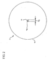
- Figure 2 is a cross-sectional side view of an optical fiber having a core (indicated in phantom) that generally defines a mode field diameter;
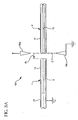
- Figure 3A illustrates a first step in the process of the invention, wherein end portions of the microstructured optical fiber illustrated in Figure 1 (and shown on the right-hand side) and the optical fiber illustrated in Figure 2 (and shown on the left-hand side) are aligned in opposing relationship within an electrically operated fusion splicer;
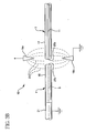
- Figure 3B illustrates a second step of the process wherein an arc generated by the fusion splicer fuses the ends of the microstructured optical fiber and the optical fiber;
- Figure 3C illustrates a third step of the inventive process wherein the fused end portions of the fibers are moved into contact with one another to form a splice
- Figure 3D illustrates a fourth step of the inventive process wherein additional heat is applied to the splice joint by the arc of the fusion splicer
- Figure 4 is a cross-sectional side view of a post-spliced end portion of a microstructured optical fiber, illustrating how the heat of fusion creates only a modest shrinkage of the holes forming the microstructure, and
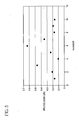
- Figure 5 is a graph illustrating the optical losses associated with each of ten sample splices formed by the process of the invention.
- the invention is both a splice and a process for joining a photonic crystal fiber 1 with a conventional optical fiber 3.
- the microstructured optical fiber 1 includes a microstructure 5 formed from a plurality of holes 7 in the glass forming the fiber 1.
- the holes 7 are parallel to the central optical axis A1 of the fiber 1, and provide a plurality of silica/air interfaces that perform a light-guiding function via total internal reflection when the fiber 1 is in use.
- the microstructure 5 is surrounded by an annular jacket 9 which, in this example, is integrally formed from the same silica forming the microstructure.
- the radial width of the jacket is at least 1.6 times the radial with of the microstructure, and is more preferably about 2.0 times this radial width.
- the radial width of the microstructured optical fiber 1 is 62.5 ⁇ m, with the microstructure 5 having a radial width of about 20.8 ⁇ m, while the jacket 9 has a radial width of 41.7 ⁇ m.
- the radial width of the jacket is slightly more than 2.0 times the radial width of the microstructure 5.
- such proportioning between the microstructure 5 and jacket 9 is important, as it helps to prevent a substantial collapse of the holes 7 forming the microstructure 5 when the splice joint of the invention is formed.
- the optical fiber 3 that the microstructured optical fiber 1 is joined to includes a core 11 surrounded by cladding 13. Both the core 11 and cladding 13 are integrally formed from silica, the difference being that the core 11 has a higher index of refraction than the surrounding cladding 13. Such a difference in the index of refraction is usually accomplished by the provision of a higher concentration of dopant atoms, such as germanium, into the core 11..
- the optical fiber 3 has a mode field diameter D2 which is somewhat larger than the diameter of the core 11 and is the same as the diameter of the mode field diameter D 1 of the microstructured optical fiber 1.
- the optical fiber 3 used in the preferred embodiment is a 2% high delta optical fiber, since such fibers typically also have a mode field diameter of approximately 6 ⁇ m, at the wavelength 1550 nm. While the invention encompasses splice joints and a splicing process wherein the mode field diameter of the optical fiber 3 is somewhat different from the mode field diameter D1 of the microstructured optical fiber 1, such an embodiment is not preferred since the geometrical mismatching of the mode field diameters will result in undesirable losses in the final splice joint.
- Figures 3A-3D illustrate the process and the resulting splice joint of the invention.
- an end portion 15 of a microstructured optical fiber 1 is placed in opposition to an end portion 17 of the optical fiber 3 within a commercially available fusion splicer 18.
- the splicer 18, may be, for example, a commercially available fusion splicer, such as, for example a Model No. FSU-975 fusion splicer manufactured by Ericsson Cable AB, available from Amherst FiberOptics of Brentwood, Tennessee. It is important that the optical axes A1 and A2 (shown in Figures 1 and 2) are collinear during this alignment step so that the mode field diameters of the fibers are precisely aligned.
- the fusion splicer 18 includes a pair of opposing, pointed electrodes 19a, b. It is further important during the initial alignment step illustrated in Figure 3A that the end 15 of the microstructured optical fiber 1 be displaced a distance d1 away from the center line C defined between the points of these electrodes 19a, b. In the process of the invention, the distance d1 ranges between about 25 to 300 ⁇ m and is preferably 100 ⁇ m.
- a carbon coating 21 is applied to the end 15 of the microstructured optical fiber 1 as shown. This coating 21 is grounded in order to facilitate the application of an arc to the end portion 15.
- the fusion splicer 18 is actuated to generate an arc 23 to create fused end portions 25a, b.
- the arc is generated from a current of between about 8 and 12 mA, and most preferably about 10 mA.
- the ends 25a, b of the fibers 1 and 3 are exposed to the resulting arc 23 for a time period of between about 0.2 and 0.4 seconds, and most preferably 0.3 seconds.
- the offset displacement of the end 25a of the microstructured optical fiber 1 the previously described distance d1 prevents the hottest portion of the arc 23 from contacting the end 25a. This is an important aspect of the invention, as such indirect contact with the arc 23 advantageously prevents excessive shrinkage of the holes 7 forming the microstructure 5.
- the third step of the process is illustrated in Figure 3C.
- the fusion splicer 18 is deactivated, and the two ends 25a, b of the fibers 1, 3 are moved together into contact to form splice joint 27.
- the ends 25a, b are moved into contact for a distance d2 of between about 6 and 10 ⁇ m, and most preferably about 8 ⁇ m.
- d2 of between about 6 and 10 ⁇ m, and most preferably about 8 ⁇ m.
- the fourth step of the splicing process is illustrated in Figure 3D.
- the fusion splicer 18 is reactivated with the same amount of current described with respect to the second process step, but for a somewhat longer fusion time of between about 0.4 and about 0.6 seconds, and most preferably for about 0.5 seconds.
- the additional heating insures the production of a strong splice, particularly between the jacket 9 of the microstructured optical fiber 1, and the cladding 13 of the optical fiber 3.
- Figure 4 illustrates the amount of hole collapse or shrinkage that typically occurs in the microstructure 29 of a microstructured optical fiber 1 at the splice joint 27. While there is some shrinkage as a result of the initial fusion step described with respect to Figure 2B, the areas of the holes 7 forming the microstructure are reduced by only about 30% from their initial cross-sectional areas.
- the relatively small amount of collapsing of the holes 7 results from the offsetting of the end 15 of the microstructured optical fiber 1 with respect to the arc generated by the fusion splicer 18 during the initial fusion step, the use of relatively small amounts of current for short amounts of time in a two-stage application of fusion heat, and the selection of a microstructured optical fiber having an outer jacket of sufficient thickness to insulate the microstructure 6 from excessive heat during the fusion steps.
- Figure 5 illustrates sample optical losses, in decibels, attributable to ten different splice joints 27 fabricated in accordance with the process of the invention. As is evident from the graph, these losses range between 0.63 dB and 0.10 dB. Considering the fact that prior splices had losses of 1.5 dB corresponding to a signal loss of about 25% and that the decibel scale is logarithmic, the invention results in a truly dramatic improvement. The highest loss among the sample splices of 0.63 dB corresponds to a loss of only about 10%, while the lowest loss of 0.10 dB corresponds to only about a 1% signal loss, which is comparable to the losses associated with splices between conventional optical fibers. Thus an improvement of between 250% and 2500% is realized.
Landscapes
- Physics & Mathematics (AREA)
- Engineering & Computer Science (AREA)
- Plasma & Fusion (AREA)
- General Physics & Mathematics (AREA)
- Optics & Photonics (AREA)
- Mechanical Coupling Of Light Guides (AREA)
- Optical Fibers, Optical Fiber Cores, And Optical Fiber Bundles (AREA)
Description
- This invention generally concerns optical splice joints, and is specifically concerned with a low loss splice joint and process for joining a microstructured optical fiber with a doped silica optical fiber.
- Microstructured optical fibers are optical waveguide fibers typically formed from silica which contain a periodic array of holes on the scale of the optical wavelengths that propagate along the axis of the fiber. The holes are symmetrically arranged within the fiber to form a light guiding microstructure or core. The resulting microstructure provides an array of air-glass interfaces that guides light along the optical axis of the fiber by total internal reflection. While such fibers are more difficult to fabricate than conventional optical fibers (some are formed by stacking, fusing and drawing a bundle of silica capillary tubes), they have the advantage of being able to transmit a broad range of different optical wavelengths in a single mode along the length of the fiber, thereby minimizing intermodal dispersion-type noise in the transmitted optical signals.
- One of the obstacles blocking the practical use of such microstructured fibers is the efficient coupling of light into and out of this type of waveguide. Such coupling is usually implemented by splices that optically and mechanically interconnect a pair of optical fibers. Such splices are typically created by a fusion splicing process wherein an electrical arc is used to fuse together the ends of optical fibers being joined.
- Unfortunately, when fusion splicing is used to join a microstructure optical fiber with a conventional optical fiber, the resulting joint causes high losses of 1.5 dB or more in the combined fiber. Such losses are far higher than the losses which occur in a splice joint between two conventional optical fibers, which typically are only about 0.02 dB, which corresponds to about a 0.5% signal loss. To put the loss problem in even greater perspective, the minimum 1.5 dB loss associated with a single microstructured optical fiber splice corresponds to at least a 25% loss in signal.
- Clearly, there is a need for a splicing process capable of reliably and consistently creating a splice joint between a microstructured optical fiber and a conventional optical fiber without the excessive losses associated with the prior art. Ideally, the resulting splice would not only have losses considerably less than the 1.5 dB associated with the prior art, but would also have a high degree of mechanical strength for resisting breakage or damage to the fiber when it is installed or modified within an optical network. Finally, it would be desirable if such a low-loss, high strength splice could be created quickly, easily, and inexpensively without the need for specially designed and manufactured fusion splicing machinery.
- By way of prior art attention is directed to the following documents, which disclose a process for forming an optical splice joint according to the preamble of
claim 1 herein. - More particularly, WO00/49435 to Russell, et al. discloses fusion splicing a photonic crystal fiber (PCF) having a plurality of holes disposed about an optical axis of the PCF to a standard (i.e. solid core and cladding) optical fiber. Russell describes varying the cross section of the PCF and the standard fibers to obtain matching mode field diameters. Russell also discloses collapsing the holes of the PCF when splicing the PCF to a standard fiber to prevent, inter alia, the holes exploding during the fusion splicing process. Van Eijkelenborg, et al. ("Optimizing holey fibre characteristics", Lasers and Electro-Optics, 2001, Cleo/Pacific Rim 2001. The 4th Pacific Rim Conference on 15-19 July 2001, Piscataway, NJ, USA, IEEE, vol. 1, 15 July 2001, pages 1436-1437, XP010566197) discloses optimizing splices between a holey fiber and a standard fiber by optimizing the varying the arrangement of holes in the holey fiber. Choi, et al. ("A new mode converter based on hollow optical fiber for gigabit LAN communication", Optical Communication, 2001. ECOC '01.27th European Conference on September 30 - October 4, 2001, Picataway, NJ, USA, IEEE, Vol. 3, 30 September 2001, pages 326-327, XP010583406 ISBN: 0-7803-6705-7) refers to fusion splicing of a standard single mode optical fiber to a hollow optical fiber for the purpose of converting the fundamental mode to a ring-shaped mode.
- The invention provides a process for forming an optical splice between (i) an end portion of a microstructured optical fiber having a light guiding microstructure region comprising a plurality of holes arranged around and parallel to an optical axis of the micro structured optical fiber, the arrangement of holes having a radial width corresponding to the maximum distance between the optical axis and the plurality of holes, the microstructure region being surrounded by a jacket, and (ii) an end portion of an optical fiber including a core surrounded by a cladding, the process comprising fusion splicing the microstructured optical fiber and the optical fiber, the process being characterized by the steps of: aligning said end portions in opposing relationship; generating a first arc from an electrically operated fusion splicer with a current of between about 8 and 12 mA; exposing said end portions to said first arc for between 0.2 and 0.4 seconds, an end of the microstructured optical fiber exposed to the first arc being offset along the optical axis of the microstructured optical fiber from a center of the first arc by a distance of between 25 µm and 300 µm; moving said opposing end portions into contact to join the microstructured optical fiber and the optical fiber and form a splice joint; and exposing the splice joint to a second arc with a current between about 8 and 12 mA for between 0.4 and 0.6 seconds; wherein the jacket has a radial width corresponding to the difference between the distance from the optical axis to an outer surface of the jacket and the radial width of the microstructured region, the radial width of the jacket being at least 1.6 times the radial width of the microstructure region, and wherein the reduction in cross sectional area of the holes during the forming of the splice joint is less than 50% after exposure of the splice joint to the second arc, relative to an initial cross sectional area of the holes.
- The optical loss associated with the fused portion is less than 1 dB and preferably less than 0.30 dB. The inventive splice and process stem from the observation by the inventors that high losses associated with some prior art microstructured optical fiber splices were caused by the substantial collapse of the holes in the microstructure during the fusion steps of the splicing process. By contrast, the holes in the microstructure in a splice of the invention are only partially collapsed by less than about 50%, and more preferably by only about 35%. This substantial reduction in hole collapse results in far smaller losses than those associated with the prior art.
- The diameter of the mode fields of both the microstructured optical fiber and optical fiber are preferably substantially equal, and the fused portion forming the splice joint has a tensile strength of at least 2.1x10⁸N/m2 (30 Kpsi) and more preferably a tensile strength equal to or greater than 3.4x10⁸/N/m2 (50 Kpsi).
- The radial width of the jacket of the microstructured optical fiber is preferably about twice the radial width of the microstructure. The optical fiber is preferably a doped silica fiber, and more preferably a 2% high delta fiber, as the mode field diameter of such fibers is about the same size as the mode field diameter of a microstructured fiber (i.e., about 6 µm).
- In the process of the invention, an end portion of a microstructured fiber and an optical fiber are first aligned in opposing relationship in a fusion splicer, with the end of the microstructured fiber offset along the axis of the fibers between 25 and 300 µm, preferably between about 75 and 120 µm from the center of the arc produced by the splicer such that the regular fiber is, preferably, an extra 75 to 120 µm over the arc. Such offsetting prevents the microstructure in the fiber end from being exposed to excessive heat. An arc is then generated from the electrically operated fusion splicer with a current of between 8 and 12 mA for a time period of between about 0.2 and 0.4 seconds, and the opposing end portions are then moved into contact. After about 0.3 seconds, the contacting end portions are then exposed to the arc for an additional time period of between about 0.3 and 0.7 seconds. The relatively thick outer jacket of the microstructured optical fiber, in combination with the offset positioning of the microstructured optical fiber end and the low current two-stage heating process prevents substantial hole collapse in the microstructure, and results in a splice that is characterized by a loss of less than 0.65 dB and more typically about 0.20 dB along with a high tensile strength.
- Figure 1 is a cross-sectional side view of a microstructured optical fiber having a centrally-disposed microstructure surrounded by a fiber jacket;
- Figure 2 is a cross-sectional side view of an optical fiber having a core (indicated in phantom) that generally defines a mode field diameter;
- Figure 3A illustrates a first step in the process of the invention, wherein end portions of the microstructured optical fiber illustrated in Figure 1 (and shown on the right-hand side) and the optical fiber illustrated in Figure 2 (and shown on the left-hand side) are aligned in opposing relationship within an electrically operated fusion splicer;
- Figure 3B illustrates a second step of the process wherein an arc generated by the fusion splicer fuses the ends of the microstructured optical fiber and the optical fiber;
- Figure 3C illustrates a third step of the inventive process wherein the fused end portions of the fibers are moved into contact with one another to form a splice;
- Figure 3D illustrates a fourth step of the inventive process wherein additional heat is applied to the splice joint by the arc of the fusion splicer;
- Figure 4 is a cross-sectional side view of a post-spliced end portion of a microstructured optical fiber, illustrating how the heat of fusion creates only a modest shrinkage of the holes forming the microstructure, and
- Figure 5 is a graph illustrating the optical losses associated with each of ten sample splices formed by the process of the invention.
- With reference now to Figures 1 and 2, wherein like numerals designate like components throughout all of the several Figures, the invention is both a splice and a process for joining a
photonic crystal fiber 1 with a conventionaloptical fiber 3. The microstructuredoptical fiber 1 includes amicrostructure 5 formed from a plurality ofholes 7 in the glass forming thefiber 1. Theholes 7 are parallel to the central optical axis A1 of thefiber 1, and provide a plurality of silica/air interfaces that perform a light-guiding function via total internal reflection when thefiber 1 is in use. Themicrostructure 5 is surrounded by anannular jacket 9 which, in this example, is integrally formed from the same silica forming the microstructure. In the preferred embodiment, the radial width of the jacket is at least 1.6 times the radial with of the microstructure, and is more preferably about 2.0 times this radial width. In the example illustrated in Figure 1, the radial width of the microstructuredoptical fiber 1 is 62.5 µm, with themicrostructure 5 having a radial width of about 20.8 µm, while thejacket 9 has a radial width of 41.7 µm. Thus, in the example illustrated in Figure 1, the radial width of the jacket is slightly more than 2.0 times the radial width of themicrostructure 5. As will become more evident hereinafter, such proportioning between themicrostructure 5 andjacket 9 is important, as it helps to prevent a substantial collapse of theholes 7 forming themicrostructure 5 when the splice joint of the invention is formed. - With specific reference to Figure 2, the
optical fiber 3 that the microstructuredoptical fiber 1 is joined to includes acore 11 surrounded by cladding 13. Both thecore 11 andcladding 13 are integrally formed from silica, the difference being that thecore 11 has a higher index of refraction than the surroundingcladding 13. Such a difference in the index of refraction is usually accomplished by the provision of a higher concentration of dopant atoms, such as germanium, into thecore 11.. In the preferred embodiment, theoptical fiber 3 has a mode field diameter D2 which is somewhat larger than the diameter of thecore 11 and is the same as the diameter of the modefield diameter D 1 of the microstructuredoptical fiber 1. Since the mode field diameter D1 of the microstructured optical fiber is approximately 6 µm at the wavelength 1550 nm, theoptical fiber 3 used in the preferred embodiment is a 2% high delta optical fiber, since such fibers typically also have a mode field diameter of approximately 6 µm, at the wavelength 1550 nm. While the invention encompasses splice joints and a splicing process wherein the mode field diameter of theoptical fiber 3 is somewhat different from the mode field diameter D1 of the microstructuredoptical fiber 1, such an embodiment is not preferred since the geometrical mismatching of the mode field diameters will result in undesirable losses in the final splice joint. - Because the mode field diameter of a 2% high delta fiber is significantly less than the mode field diameter of commonly used optical fibers such as SMF-28® single mode optical fiber manufactured by Coming, Incorporated, of Coming, New York, there is a need for an economical and efficient way to splice together optical fibers having relatively small mode field diameters (i.e., on the order of 6 µm) with more commonly used fibers such as SMF-28® single mode optical fiber having larger mode field diameters (i.e., on the order of about 10 µm). Fortunately, this problem has already been solved in a patent application entitled "An Optical Fiber Having an Expanded Mode Field Diameter and Method for Expanding the Mode Field Diameter," invented by Qui Wu, PCT Serial No. US99/21828 assigned to Coming, Incorporated. This patent application has been published under International Publication No. WO 00/19256. This application provides a complete description as to how a bridging fiber might be fabricated that has an expanding mode field diameter between 6 µm at one end, and 10 µm on the other end which might be used to efficiently splice couple a segment of
high delta 2% fiber to SMF-28® single mode optical fiber. - Figures 3A-3D illustrate the process and the resulting splice joint of the invention. In the first step of the process illustrated in Figure 3A, an
end portion 15 of a microstructuredoptical fiber 1 is placed in opposition to anend portion 17 of theoptical fiber 3 within a commerciallyavailable fusion splicer 18. Thesplicer 18, may be, for example, a commercially available fusion splicer, such as, for example a Model No. FSU-975 fusion splicer manufactured by Ericsson Cable AB, available from Amherst FiberOptics of Brentwood, Tennessee. It is important that the optical axes A1 and A2 (shown in Figures 1 and 2) are collinear during this alignment step so that the mode field diameters of the fibers are precisely aligned. As is shown throughout Figures 3A-3D, thefusion splicer 18 includes a pair of opposing, pointedelectrodes 19a, b. It is further important during the initial alignment step illustrated in Figure 3A that theend 15 of the microstructuredoptical fiber 1 be displaced a distance d1 away from the center line C defined between the points of theseelectrodes 19a, b. In the process of the invention, the distance d1 ranges between about 25 to 300 µm and is preferably 100 µm. Prior to the application of an arc from theelectrodes 19a,b a carbon coating 21 is applied to theend 15 of the microstructuredoptical fiber 1 as shown. Thiscoating 21 is grounded in order to facilitate the application of an arc to theend portion 15. - In the second step of the splicing process illustrated in Figure 3B, the
fusion splicer 18 is actuated to generate anarc 23 to create fusedend portions 25a, b. In the preferred implementation of this process step, the arc is generated from a current of between about 8 and 12 mA, and most preferably about 10 mA. Moreover, theends 25a, b of thefibers arc 23 for a time period of between about 0.2 and 0.4 seconds, and most preferably 0.3 seconds. The offset displacement of theend 25a of the microstructuredoptical fiber 1 the previously described distance d1 prevents the hottest portion of thearc 23 from contacting theend 25a. This is an important aspect of the invention, as such indirect contact with thearc 23 advantageously prevents excessive shrinkage of theholes 7 forming themicrostructure 5. - The third step of the process is illustrated in Figure 3C. Here, the
fusion splicer 18 is deactivated, and the twoends 25a, b of thefibers ends 25a, b are moved into contact for a distance d2 of between about 6 and 10 µm, and most preferably about 8 µm. Such a "overlapping" contact is possible since theends 25a, b of thefibers - The fourth step of the splicing process is illustrated in Figure 3D. Here, between about 0.2 and 0.5 seconds after the two
ends 25a, b are brought into contact to form thesplice 27, thefusion splicer 18 is reactivated with the same amount of current described with respect to the second process step, but for a somewhat longer fusion time of between about 0.4 and about 0.6 seconds, and most preferably for about 0.5 seconds. The additional heating insures the production of a strong splice, particularly between thejacket 9 of the microstructuredoptical fiber 1, and thecladding 13 of theoptical fiber 3. - Figure 4 illustrates the amount of hole collapse or shrinkage that typically occurs in the
microstructure 29 of a microstructuredoptical fiber 1 at the splice joint 27. While there is some shrinkage as a result of the initial fusion step described with respect to Figure 2B, the areas of theholes 7 forming the microstructure are reduced by only about 30% from their initial cross-sectional areas. The applicants believe that the relatively small amount of collapsing of theholes 7 results from the offsetting of theend 15 of the microstructuredoptical fiber 1 with respect to the arc generated by thefusion splicer 18 during the initial fusion step, the use of relatively small amounts of current for short amounts of time in a two-stage application of fusion heat, and the selection of a microstructured optical fiber having an outer jacket of sufficient thickness to insulate themicrostructure 6 from excessive heat during the fusion steps. - Figure 5 illustrates sample optical losses, in decibels, attributable to ten
different splice joints 27 fabricated in accordance with the process of the invention. As is evident from the graph, these losses range between 0.63 dB and 0.10 dB. Considering the fact that prior splices had losses of 1.5 dB corresponding to a signal loss of about 25% and that the decibel scale is logarithmic, the invention results in a truly dramatic improvement. The highest loss among the sample splices of 0.63 dB corresponds to a loss of only about 10%, while the lowest loss of 0.10 dB corresponds to only about a 1% signal loss, which is comparable to the losses associated with splices between conventional optical fibers. Thus an improvement of between 250% and 2500% is realized. - While this invention has been described with respect to preferred embodiments, various additions, modifications, and variations of the invention will become evident to persons of ordinary skill in the art. All such additions, modifications, and variations are intended to be encompassed within the scope of this patent, which is limited only by the claims of appended hereto.
-
- 1.
- Microstructured optical fiber
- 3.
- Conventional optical fiber
- 5.
- Microstructure
- 7.
- Holes
- 9.
- Jacket
- 11.
- Core
- 13.
- Cladding
- 15.
- End portion (of microstructured optical fiber)
- 17.
- End portion (of optical fiber)
- 18.
- Fusion splicer
- 19.
- Electrodes a, b
- 21.
- Carbon coating
- 23.
- Arc
- 25.
- Fused end portions a, b
- 27.
- Splice
- 29.
- Post-fusion microstructure
Claims (6)
- A process for forming an optical splice between(i) an end portion (15) of a microstructured optical fiber (1) having a light guiding microstructure region (5) comprising a plurality of holes (7) arranged around and parallel to an optical axis (A1) of the microstructured optical fiber, the arrangement of holes having a radial width corresponding to the maximum distance between the optical axis and the plurality of holes, the microstructure region being surrounded by a jacket (9), and(ii) an end portion (17) of an optical fiber (3) including a core (11) surrounded by a cladding (13),the process comprising fusion splicing the micro structured optical fiber (1) and the optical fiber (3), the process being characterized by the steps of:aligning said end portions in opposing relationship;generating a first arc from an electrically operated fusion splicer (18) with a current of between about 8 and 12 mA;exposing said end portions to said first arc for between 0.2 and 0.4 seconds, an end (25a) of the microstructured optical fiber (1) exposed to the first arc being offset along the optical axis of the microstructured optical fiber from a center of the first arc by a distance (d1) of between 25 µm and 300 µm;moving said opposing end portions into contact to join the microstructured optical fiber (1) and the optical fiber (3) and form a splice joint (27); andexposing the splice joint to a second arc with a current between about 8 and 12 mA for between 0.4 and 0.6 seconds;wherein the jacket (9) has a radial width (R) corresponding to the difference between the distance from the optical axis to an outer surface of the jacket and the radial width of the microstructured region (5), the radial width (R) of the jacket being at least 1.6 times the radial width of the microstructure region (5), and wherein the reduction in cross sectional area of the holes (7) during the forming of the splice joint (27) is less than 50% after exposure of the splice joint to the second arc, relative to an initial cross sectional area of the holes.
- The process of forming an optical splice defined in claim 1, further comprising coating the end portion of the microstructured optical fiber with a carbon coating (21) and grounding the carbon coating prior to generating the first are.
- The process according to any preceding claim, wherein the mode field diameter of the microstructured optical fiber (1) is substantially equal to the mode field diameter of the optical fiber (3).
- The process according to any preceding claim, wherein the joined fibers exhibit an optical loss between 0.10 dB and 0.63 dB at the splice joint (27).
- The process according to any preceding claim, wherein the mode field diameter of the microstructured optical fiber is approximately 6 µm at a wavelength of 1550 µm.
- The process according to any preceding claim, wherein the said offset distance (d1) is from 75 to 120 µm.
Applications Claiming Priority (3)
| Application Number | Priority Date | Filing Date | Title |
|---|---|---|---|
| US10/004,375 US6652163B2 (en) | 2001-10-31 | 2001-10-31 | Splice joint and process for joining a microstructured optical fiber and a conventional optical fiber |
| US4375 | 2001-10-31 | ||
| PCT/US2002/032081 WO2003038496A1 (en) | 2001-10-31 | 2002-10-07 | Splice joint and process for joining a microstructured optical fiber and a conventional optical fiber |
Publications (3)
| Publication Number | Publication Date |
|---|---|
| EP1440338A1 EP1440338A1 (en) | 2004-07-28 |
| EP1440338A4 EP1440338A4 (en) | 2005-08-03 |
| EP1440338B1 true EP1440338B1 (en) | 2007-05-23 |
Family
ID=21710488
Family Applications (1)
| Application Number | Title | Priority Date | Filing Date |
|---|---|---|---|
| EP02802433A Expired - Lifetime EP1440338B1 (en) | 2001-10-31 | 2002-10-07 | Splice joint and process for joining a microstructured optical fiber and a conventional optical fiber |
Country Status (5)
| Country | Link |
|---|---|
| US (1) | US6652163B2 (en) |
| EP (1) | EP1440338B1 (en) |
| JP (2) | JP2005508020A (en) |
| DE (1) | DE60220302T2 (en) |
| WO (1) | WO2003038496A1 (en) |
Families Citing this family (45)
| Publication number | Priority date | Publication date | Assignee | Title |
|---|---|---|---|---|
| EP1255139A1 (en) * | 2001-05-03 | 2002-11-06 | Corning Incorporated | Method and apparatus for splicing optical fibres |
| AU782604B2 (en) * | 2001-05-22 | 2005-08-11 | Sumitomo Electric Industries, Ltd. | Method for fusion splicing optical fibers and apparatus for heating spliced part by arc |
| US6866429B2 (en) * | 2001-09-26 | 2005-03-15 | Np Photonics, Inc. | Method of angle fusion splicing silica fiber with low-temperature non-silica fiber |
| US6705771B2 (en) * | 2001-09-26 | 2004-03-16 | Np Photonics, Inc. | Method of fusion splicing silica fiber with low-temperature multi-component glass fiber |
| US6652163B2 (en) * | 2001-10-31 | 2003-11-25 | Corning Incorporated | Splice joint and process for joining a microstructured optical fiber and a conventional optical fiber |
| AU2003281985A1 (en) | 2002-11-23 | 2004-06-18 | Crystal Fibre A/S | Splicing and connectorization of photonic crystal fibres |
| US7207732B2 (en) * | 2003-06-04 | 2007-04-24 | Corning Incorporated | Coated optical fiber and curable compositions suitable for coating optical fiber |
| US20050008291A1 (en) * | 2003-07-08 | 2005-01-13 | Baney Dougas M. | Optical wave-guide microstructured environment absorption cell |
| US6993228B2 (en) | 2003-08-13 | 2006-01-31 | Corning Incorporated | Dispersion compensated optical fiber transmission system and module including micro-structured optical fiber |
| DE10340964A1 (en) * | 2003-09-05 | 2005-03-31 | Leica Microsystems Heidelberg Gmbh | Light source with a microstructured optical element |
| US7280730B2 (en) * | 2004-01-16 | 2007-10-09 | Imra America, Inc. | Large core holey fibers |
| JP3964454B2 (en) * | 2004-06-22 | 2007-08-22 | 株式会社フジクラ | Photonic crystal fiber connection method |
| US7209619B2 (en) | 2004-12-30 | 2007-04-24 | Imra America, Inc. | Photonic bandgap fibers |
| US7787729B2 (en) | 2005-05-20 | 2010-08-31 | Imra America, Inc. | Single mode propagation in fibers and rods with large leakage channels |
| US20080037939A1 (en) * | 2006-07-31 | 2008-02-14 | The Hong Kong Polytechnic University | Splicing small core photonic crystal fibers and conventional single mode fiber |
| EP1921475A1 (en) * | 2006-11-09 | 2008-05-14 | CCS Technology, Inc. | Method for detecting a core of an optical fiber and method and apparatus for connecting optical fibers |
| US7458734B2 (en) * | 2006-11-09 | 2008-12-02 | Corning Incorporated | Method of splicing an optical fiber with holes in the cladding |
| US7822310B2 (en) * | 2007-02-28 | 2010-10-26 | Corning Cable Systems Llc | Fiber optic splice trays |
| US8798427B2 (en) | 2007-09-05 | 2014-08-05 | Corning Cable Systems Llc | Fiber optic terminal assembly |
| WO2009042347A1 (en) * | 2007-09-26 | 2009-04-02 | Imra America, Inc. | Glass large-core optical fibers |
| US7742670B2 (en) * | 2007-10-01 | 2010-06-22 | Corning Cable Systems Llc | Index-matching gel for nanostructure optical fibers and mechanical splice assembly and connector using same |
| US7628548B2 (en) * | 2007-10-01 | 2009-12-08 | Corning Cable Systems Llc | Index-matching gel for nanostructure optical fibers and mechanical splice assembly and connector using same |
| EP2172795A1 (en) * | 2008-10-02 | 2010-04-07 | CCS Technology Inc. | Method of splicing microstructured optical fibers |
| WO2010040256A1 (en) | 2008-10-09 | 2010-04-15 | Corning Cable Systems Llc | Fiber optic terminal having adapter panel supporting both input and output fibers from an optical splitter |
| US8879882B2 (en) | 2008-10-27 | 2014-11-04 | Corning Cable Systems Llc | Variably configurable and modular local convergence point |
| US8055110B2 (en) * | 2008-11-17 | 2011-11-08 | Corning Incorporated | Bend insensitive fiber with reduced heat induced loss |
| EP2237091A1 (en) | 2009-03-31 | 2010-10-06 | Corning Cable Systems LLC | Removably mountable fiber optic terminal |
| US8467651B2 (en) | 2009-09-30 | 2013-06-18 | Ccs Technology Inc. | Fiber optic terminals configured to dispose a fiber optic connection panel(s) within an optical fiber perimeter and related methods |
| TWI416183B (en) * | 2010-03-11 | 2013-11-21 | Univ Nat Sun Yat Sen | Crystal fiber fusing method |
| US9547144B2 (en) | 2010-03-16 | 2017-01-17 | Corning Optical Communications LLC | Fiber optic distribution network for multiple dwelling units |
| US8792767B2 (en) | 2010-04-16 | 2014-07-29 | Ccs Technology, Inc. | Distribution device |
| JP2012083635A (en) * | 2010-10-14 | 2012-04-26 | Sei Optifrontier Co Ltd | Optical fiber fusion splicing method |
| US9547145B2 (en) | 2010-10-19 | 2017-01-17 | Corning Optical Communications LLC | Local convergence point for multiple dwelling unit fiber optic distribution network |
| US9219546B2 (en) | 2011-12-12 | 2015-12-22 | Corning Optical Communications LLC | Extremely high frequency (EHF) distributed antenna systems, and related components and methods |
| US10110307B2 (en) | 2012-03-02 | 2018-10-23 | Corning Optical Communications LLC | Optical network units (ONUs) for high bandwidth connectivity, and related components and methods |
| US9004778B2 (en) | 2012-06-29 | 2015-04-14 | Corning Cable Systems Llc | Indexable optical fiber connectors and optical fiber connector arrays |
| US9049500B2 (en) | 2012-08-31 | 2015-06-02 | Corning Cable Systems Llc | Fiber optic terminals, systems, and methods for network service management |
| US8909019B2 (en) | 2012-10-11 | 2014-12-09 | Ccs Technology, Inc. | System comprising a plurality of distribution devices and distribution device |
| EP3331833B1 (en) * | 2015-06-17 | 2023-07-26 | Corning Incorporated | Re-coated optical fibers and methods of re-coating optical fibers |
| US10078181B2 (en) * | 2015-11-03 | 2018-09-18 | Triad Technology, Inc. | Robust fiber cell for atomic and molecular sensing |
| CN106249353B (en) * | 2016-07-27 | 2019-11-08 | 北京航空航天大学 | A kind of high intensity hollow-core photonic crystal fiber welding process |
| US10209187B1 (en) | 2018-08-22 | 2019-02-19 | Triad Technology, Inc. | Method for atomic and molecular sensing |
| GB201911183D0 (en) * | 2019-08-05 | 2019-09-18 | Lumenisity Ltd | Optical fibre splicing method |
| EP4330745A1 (en) * | 2021-04-29 | 2024-03-06 | Ram Photonics Industrial, LLC | Method and system for rotational alignment of polarization maintaining fibers |
| CN114560628B (en) * | 2022-03-21 | 2023-05-26 | 创昇光电科技(苏州)有限公司 | Preparation method of local three-dimensional microstructure optical fiber |
Family Cites Families (16)
| Publication number | Priority date | Publication date | Assignee | Title |
|---|---|---|---|---|
| US4689065A (en) * | 1986-02-14 | 1987-08-25 | American Telephone And Telegraph Company, At&T Bell Laboratories | Optical waveguide glass fiber flame processing |
| JPS63157110A (en) * | 1986-12-22 | 1988-06-30 | Nippon Telegr & Teleph Corp <Ntt> | Method for fusion splicing fluoride optical fibers |
| JPH01284806A (en) * | 1988-05-12 | 1989-11-16 | Fujitsu Ltd | Erasing method for flaw on surface of optical fiber |
| JP2797335B2 (en) * | 1988-09-24 | 1998-09-17 | 住友電気工業株式会社 | Splicing method of hermetic coated optical fiber |
| JPH04315107A (en) * | 1991-04-12 | 1992-11-06 | Sumitomo Electric Ind Ltd | Method for connecting optical fiber |
| US6404966B1 (en) * | 1998-05-07 | 2002-06-11 | Nippon Telegraph And Telephone Corporation | Optical fiber |
| US6481903B1 (en) * | 1998-08-07 | 2002-11-19 | Tycom (U.S.) Inc. | Optical fiber splice protector and method for applying same |
| US6275627B1 (en) * | 1998-09-25 | 2001-08-14 | Corning Incorporated | Optical fiber having an expanded mode field diameter and method of expanding the mode field diameter of an optical fiber |
| GB9903918D0 (en) * | 1999-02-19 | 1999-04-14 | Univ Bath | Improvements in and relating to photonic crystal fibres |
| JP4104769B2 (en) * | 1999-02-25 | 2008-06-18 | 株式会社フジクラ | Optical fiber fusion splicer |
| IES990889A2 (en) * | 1999-10-22 | 2001-05-02 | Viveen Ltd | Jointed optical fibers |
| JP3815170B2 (en) * | 2000-02-14 | 2006-08-30 | 住友電気工業株式会社 | Microstructured optical fiber preform and method of manufacturing microstructured optical fiber |
| US6788865B2 (en) * | 2000-03-03 | 2004-09-07 | Nippon Telegraph And Telephone Corporation | Polarization maintaining optical fiber with improved polarization maintaining property |
| JP2002006167A (en) * | 2000-06-19 | 2002-01-09 | Fujikura Ltd | Optical fiber fusion splicing machine |
| JP3756056B2 (en) * | 2000-11-09 | 2006-03-15 | 三菱電線工業株式会社 | Photonic crystal fiber fusion method |
| US6652163B2 (en) * | 2001-10-31 | 2003-11-25 | Corning Incorporated | Splice joint and process for joining a microstructured optical fiber and a conventional optical fiber |
-
2001
- 2001-10-31 US US10/004,375 patent/US6652163B2/en not_active Expired - Lifetime
-
2002
- 2002-10-07 JP JP2003540708A patent/JP2005508020A/en active Pending
- 2002-10-07 WO PCT/US2002/032081 patent/WO2003038496A1/en active IP Right Grant
- 2002-10-07 EP EP02802433A patent/EP1440338B1/en not_active Expired - Lifetime
- 2002-10-07 DE DE60220302T patent/DE60220302T2/en not_active Expired - Lifetime
-
2010
- 2010-07-23 JP JP2010165720A patent/JP5514031B2/en not_active Expired - Lifetime
Non-Patent Citations (1)
| Title |
|---|
| None * |
Also Published As
| Publication number | Publication date |
|---|---|
| EP1440338A1 (en) | 2004-07-28 |
| JP2005508020A (en) | 2005-03-24 |
| US20030081915A1 (en) | 2003-05-01 |
| DE60220302T2 (en) | 2008-01-17 |
| US6652163B2 (en) | 2003-11-25 |
| JP5514031B2 (en) | 2014-06-04 |
| JP2010286842A (en) | 2010-12-24 |
| EP1440338A4 (en) | 2005-08-03 |
| WO2003038496A1 (en) | 2003-05-08 |
| DE60220302D1 (en) | 2007-07-05 |
Similar Documents
| Publication | Publication Date | Title |
|---|---|---|
| EP1440338B1 (en) | Splice joint and process for joining a microstructured optical fiber and a conventional optical fiber | |
| US7991255B2 (en) | Means of coupling light into optical fibers and methods of manufacturing a coupler | |
| US6275627B1 (en) | Optical fiber having an expanded mode field diameter and method of expanding the mode field diameter of an optical fiber | |
| US20110280517A1 (en) | Techniques and devices for low-loss, modefield matched coupling to a multicore fiber | |
| JPS63502460A (en) | Technology to reduce fiber connection loss | |
| WO2005052640A2 (en) | Optical fiber pump multiplexer | |
| WO2005124409A1 (en) | Connecting method and structure of photonic crystal fiber | |
| EP0635140B1 (en) | One by eight optical fiber coupler | |
| US7609928B2 (en) | Method of connecting optical fibers | |
| US5408556A (en) | 1 X N splitter for single-mode fibers and method of construction | |
| WO2005022217A1 (en) | Fiber optics transmission line | |
| WO2006006604A1 (en) | Hole assist type holey fiber and low bending loss multimode holey fiber | |
| AU700855B2 (en) | Low loss fiber optic coupler and method | |
| US5035477A (en) | Method of changing the spot diameter of single-mode step-index fibers, and single-mode fiber coupling unit made by said method | |
| US20030180016A1 (en) | Method of splicing optical fibers and multi-fiber component | |
| JP4823759B2 (en) | Optical fiber connector manufacturing method | |
| US20040052485A1 (en) | Terminating polymer optical fibre | |
| EP0780709B1 (en) | Broadband coupler | |
| JP4690249B2 (en) | Highly flexible optical fiber | |
| JPH0766092B2 (en) | Mode conversion code | |
| JP3940066B2 (en) | Fusion splicing method of photonic crystal fiber | |
| JP2004191760A (en) | Fusion splicing method of photonic crystal fiber | |
| JP2000206361A (en) | Optical fiber type multi-branch coupler, and manufacture thereof | |
| JPH02141707A (en) | Fiber type coupler and manufacture thereof | |
| JP2005345516A (en) | Manufacturing method of optical fiber coupler |
Legal Events
| Date | Code | Title | Description |
|---|---|---|---|
| PUAI | Public reference made under article 153(3) epc to a published international application that has entered the european phase |
Free format text: ORIGINAL CODE: 0009012 |
|
| 17P | Request for examination filed |
Effective date: 20040413 |
|
| AK | Designated contracting states |
Kind code of ref document: A1 Designated state(s): AT BE BG CH CY CZ DE DK EE ES FI FR GB GR IE IT LI LU MC NL PT SE SK TR |
|
| AX | Request for extension of the european patent |
Extension state: AL LT LV MK RO SI |
|
| A4 | Supplementary search report drawn up and despatched |
Effective date: 20050620 |
|
| RIC1 | Information provided on ipc code assigned before grant |
Ipc: G02B 6/255 20060101AFI20060829BHEP Ipc: G02B 6/02 20060101ALI20060829BHEP |
|
| GRAP | Despatch of communication of intention to grant a patent |
Free format text: ORIGINAL CODE: EPIDOSNIGR1 |
|
| GRAS | Grant fee paid |
Free format text: ORIGINAL CODE: EPIDOSNIGR3 |
|
| GRAA | (expected) grant |
Free format text: ORIGINAL CODE: 0009210 |
|
| AK | Designated contracting states |
Kind code of ref document: B1 Designated state(s): DE FR GB IT NL |
|
| REG | Reference to a national code |
Ref country code: GB Ref legal event code: FG4D |
|
| REF | Corresponds to: |
Ref document number: 60220302 Country of ref document: DE Date of ref document: 20070705 Kind code of ref document: P |
|
| NLV1 | Nl: lapsed or annulled due to failure to fulfill the requirements of art. 29p and 29m of the patents act | ||
| ET | Fr: translation filed | ||
| PG25 | Lapsed in a contracting state [announced via postgrant information from national office to epo] |
Ref country code: NL Free format text: LAPSE BECAUSE OF FAILURE TO SUBMIT A TRANSLATION OF THE DESCRIPTION OR TO PAY THE FEE WITHIN THE PRESCRIBED TIME-LIMIT Effective date: 20070523 |
|
| PLBE | No opposition filed within time limit |
Free format text: ORIGINAL CODE: 0009261 |
|
| STAA | Information on the status of an ep patent application or granted ep patent |
Free format text: STATUS: NO OPPOSITION FILED WITHIN TIME LIMIT |
|
| 26N | No opposition filed |
Effective date: 20080226 |
|
| PG25 | Lapsed in a contracting state [announced via postgrant information from national office to epo] |
Ref country code: IT Free format text: LAPSE BECAUSE OF FAILURE TO SUBMIT A TRANSLATION OF THE DESCRIPTION OR TO PAY THE FEE WITHIN THE PRESCRIBED TIME-LIMIT Effective date: 20070523 |
|
| GBPC | Gb: european patent ceased through non-payment of renewal fee |
Effective date: 20071007 |
|
| PG25 | Lapsed in a contracting state [announced via postgrant information from national office to epo] |
Ref country code: GB Free format text: LAPSE BECAUSE OF NON-PAYMENT OF DUE FEES Effective date: 20071007 |
|
| PGFP | Annual fee paid to national office [announced via postgrant information from national office to epo] |
Ref country code: FR Payment date: 20101105 Year of fee payment: 9 |
|
| REG | Reference to a national code |
Ref country code: FR Ref legal event code: ST Effective date: 20120629 |
|
| PG25 | Lapsed in a contracting state [announced via postgrant information from national office to epo] |
Ref country code: FR Free format text: LAPSE BECAUSE OF NON-PAYMENT OF DUE FEES Effective date: 20111102 |
|
| PGFP | Annual fee paid to national office [announced via postgrant information from national office to epo] |
Ref country code: DE Payment date: 20151028 Year of fee payment: 14 |
|
| REG | Reference to a national code |
Ref country code: DE Ref legal event code: R119 Ref document number: 60220302 Country of ref document: DE |
|
| PG25 | Lapsed in a contracting state [announced via postgrant information from national office to epo] |
Ref country code: DE Free format text: LAPSE BECAUSE OF NON-PAYMENT OF DUE FEES Effective date: 20170503 |