EP1439744A2 - Apparatus and method for aligning and attaching solder columns to a substrate - Google Patents
Apparatus and method for aligning and attaching solder columns to a substrate Download PDFInfo
- Publication number
- EP1439744A2 EP1439744A2 EP04250191A EP04250191A EP1439744A2 EP 1439744 A2 EP1439744 A2 EP 1439744A2 EP 04250191 A EP04250191 A EP 04250191A EP 04250191 A EP04250191 A EP 04250191A EP 1439744 A2 EP1439744 A2 EP 1439744A2
- Authority
- EP
- European Patent Office
- Prior art keywords
- alignment plate
- electrical contacts
- substrate
- solder
- solder columns
- Prior art date
- Legal status (The legal status is an assumption and is not a legal conclusion. Google has not performed a legal analysis and makes no representation as to the accuracy of the status listed.)
- Withdrawn
Links
Images




Classifications
-
- H—ELECTRICITY
- H05—ELECTRIC TECHNIQUES NOT OTHERWISE PROVIDED FOR
- H05K—PRINTED CIRCUITS; CASINGS OR CONSTRUCTIONAL DETAILS OF ELECTRIC APPARATUS; MANUFACTURE OF ASSEMBLAGES OF ELECTRICAL COMPONENTS
- H05K3/00—Apparatus or processes for manufacturing printed circuits
- H05K3/30—Assembling printed circuits with electric components, e.g. with resistors
- H05K3/32—Assembling printed circuits with electric components, e.g. with resistors electrically connecting electric components or wires to printed circuits
- H05K3/34—Assembling printed circuits with electric components, e.g. with resistors electrically connecting electric components or wires to printed circuits by soldering
- H05K3/3465—Application of solder
- H05K3/3478—Application of solder preforms; Transferring prefabricated solder patterns
-
- H—ELECTRICITY
- H10—SEMICONDUCTOR DEVICES; ELECTRIC SOLID-STATE DEVICES NOT OTHERWISE PROVIDED FOR
- H10W—GENERIC PACKAGES, INTERCONNECTIONS, CONNECTORS OR OTHER CONSTRUCTIONAL DETAILS OF DEVICES COVERED BY CLASS H10
- H10W72/00—Interconnections or connectors in packages
- H10W72/071—Connecting or disconnecting
-
- H—ELECTRICITY
- H10—SEMICONDUCTOR DEVICES; ELECTRIC SOLID-STATE DEVICES NOT OTHERWISE PROVIDED FOR
- H10W—GENERIC PACKAGES, INTERCONNECTIONS, CONNECTORS OR OTHER CONSTRUCTIONAL DETAILS OF DEVICES COVERED BY CLASS H10
- H10W70/00—Package substrates; Interposers; Redistribution layers [RDL]
- H10W70/01—Manufacture or treatment
- H10W70/05—Manufacture or treatment of insulating or insulated package substrates, or of interposers, or of redistribution layers
- H10W70/093—Connecting or disconnecting other interconnections thereto or therefrom, e.g. connecting bond wires or bumps
-
- H—ELECTRICITY
- H05—ELECTRIC TECHNIQUES NOT OTHERWISE PROVIDED FOR
- H05K—PRINTED CIRCUITS; CASINGS OR CONSTRUCTIONAL DETAILS OF ELECTRIC APPARATUS; MANUFACTURE OF ASSEMBLAGES OF ELECTRICAL COMPONENTS
- H05K2203/00—Indexing scheme relating to apparatus or processes for manufacturing printed circuits covered by H05K3/00
- H05K2203/01—Tools for processing; Objects used during processing
- H05K2203/0195—Tool for a process not provided for in H05K3/00, e.g. tool for handling objects using suction, for deforming objects, for applying local pressure
-
- H—ELECTRICITY
- H05—ELECTRIC TECHNIQUES NOT OTHERWISE PROVIDED FOR
- H05K—PRINTED CIRCUITS; CASINGS OR CONSTRUCTIONAL DETAILS OF ELECTRIC APPARATUS; MANUFACTURE OF ASSEMBLAGES OF ELECTRICAL COMPONENTS
- H05K2203/00—Indexing scheme relating to apparatus or processes for manufacturing printed circuits covered by H05K3/00
- H05K2203/04—Soldering or other types of metallurgic bonding
- H05K2203/0415—Small preforms other than balls, e.g. discs, cylinders or pillars
-
- H—ELECTRICITY
- H05—ELECTRIC TECHNIQUES NOT OTHERWISE PROVIDED FOR
- H05K—PRINTED CIRCUITS; CASINGS OR CONSTRUCTIONAL DETAILS OF ELECTRIC APPARATUS; MANUFACTURE OF ASSEMBLAGES OF ELECTRICAL COMPONENTS
- H05K2203/00—Indexing scheme relating to apparatus or processes for manufacturing printed circuits covered by H05K3/00
- H05K2203/05—Patterning and lithography; Masks; Details of resist
- H05K2203/0548—Masks
- H05K2203/0557—Non-printed masks
-
- H—ELECTRICITY
- H05—ELECTRIC TECHNIQUES NOT OTHERWISE PROVIDED FOR
- H05K—PRINTED CIRCUITS; CASINGS OR CONSTRUCTIONAL DETAILS OF ELECTRIC APPARATUS; MANUFACTURE OF ASSEMBLAGES OF ELECTRICAL COMPONENTS
- H05K2203/00—Indexing scheme relating to apparatus or processes for manufacturing printed circuits covered by H05K3/00
- H05K2203/08—Treatments involving gases
- H05K2203/082—Suction, e.g. for holding solder balls or components
Definitions
- the present invention relates an apparatus and method for aligning, placing and attaching a plurality of solder columns to a patterned array of electrical terminals or conductive pads on a ceramic substrate.
- a ball grid array package wherein one or more chips are mounted on the top surface of a substrate.
- the ball grid array package uses an array of solder balls to provide electrical connections between the substrate and a printed circuit board.
- a problem with this type of package is that substantial differences in the thermal coefficient of expansion can exist between the substrate and the printed circuit board. Such differences in the thermal coefficient of expansion cause plastic deformation of the solder balls.
- the column grid array package uses an array of solder columns to make electrical connections between a ceramic substrate and a printed circuit board.
- the solder columns typically have a height of approximately 2.55 mm and a diameter of 0.50 mm.
- the taller configuration of the solder columns offers compliancy to better absorb the differential thermal expansion rate between the ceramic column grid array package and the printed circuit board.
- a low melting temperature solder paste is deposited on electrically conductive contact pads which are placed on one side of the ceramic substrate.
- the solder columns typically made from a high melting temperature solder using a nominal 90/10 alloy of lead to tin, are vertically positioned on the corresponding contact pads. The combination is then heated in a reflow oven so that the solder paste is reflowed to make a mechanical and electrical connection between the solder columns and the pads.
- a vacuum pickup tool is typically used to pick up and place a multiplicity of solder balls in the desired pattern on a semiconductor substrate.
- the spherical shape of the solder balls makes it easier to pick up and place a full array of solder balls on the substrate.
- solder columns have a cylindrical shape and must, therefore, be placed in an upright orientation when the solder columns are attached to corresponding conductive pads on a ceramic substrate.
- an apparatus for aligning and attaching a plurality of solder columns to a patterned array of corresponding electrical contacts on a ceramic substrate includes a substantially flat alignment plate having a plurality of through holes defined in a pattern identical to the pattern of the electrical contacts and adapted to allow the solder columns to vertically pass therethrough. At least one retainer depends from the alignment plate and adapted to hold the alignment plate in a fixed position above the ceramic substrate such that the through holes are vertically aligned with the corresponding electrical contacts. In one embodiment, four retainers are attached to the respective four sides of the rectangular alignment plate.
- the alignment plate is preferably made of a refractory material such as titanium.
- a vacuum pickup tool may be used to deliver an array of solder columns to the alignment plate.
- the vacuum pickup tool includes a vacuum head and a carrier projection extending from the bottom of the vacuum head.
- a series of cavities are defined in the carrier projection and each have vacuum ports communicated with a vacuum source. The cavities are spaced from each other a distance equal to the distance between each adjacent through holes of the alignment plate.
- a method for aligning and attaching a plurality of solder columns to a patterned array of corresponding electrical contacts on a substrate includes the step of providing a substantially flat alignment plate including a plurality of through holes defined in a pattern identical to the pattern of the electrical contacts.
- a solder paste is screen printed or otherwise applied onto the electrical contacts.
- the alignment plate is held in a fixed position above the substrate such that the through holes are vertically aligned with the electrical pads.
- the solder columns are inserted through the through holes of the alignment plate. This allows the solder columns to be placed in an upright orientation on the electrical contacts.
- the alignment plate and the substrate are passed through a reflow oven so as to reflow or melt the solder paste.
- the solder paste is thereafter resolidified to make a bond between the solder columns and the corresponding electrical contacts.
- the alignment plate is removed from the substrate after the solder columns are attached to all the electrical contacts on the ceramic substrate.
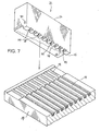
- the apparatus 10 includes a substantially flat alignment plate 12 in which a plurality of through holes 14 are defined in a patterned array.
- the alignment plate 12 is square or rectangular in shape and has four sides 16.
- the alignment plate 12 has a thickness of at least 0. 5 mm.
- the alignment plate 12 is preferably made of titanium to provide better resistance to heat.
- the alignment plate 12 may be made of any other suitable refractory materials such as titanium alloy, ceramic, stainless steel, engineering plastics, carbon, carbide and nitride.
- four retainers 18 depend from intermediate the four respective sides 16 of the alignment plate 12.
- the retainers 18 each have a step 20.
- the steps 20 are sized and configured to engage the upper peripheral edge of a substrate 22, as shown better in Figs. 3 and 4. Although not shown, four angled retainers may alternatively be attached to the four corners of the alignment plate 12.
- the alignment plate 12 has a size substantially equal to the size of the substrate.
- the substrate 22 is typically made of ceramic.
- the ceramic substrate 22 has a plurality of electrically conductive pads or contacts 24 arranged in a pattern identical to the pattern of the through holes 14 of the alignment plate 12. The number of the through holes 14 is equal to the number of the conductive pads 24.
- Figs 2 to 6 sequentially illustrate the manner in which an array of solder columns 26 are attached to the conductive pads 24 on the ceramic substrate 22.
- a solder paste 28 is screen printed onto all the conductive pads 24.
- the alignment plate 12 is then mounted over the ceramic substrate 22 as shown in Fig. 3.
- the retainers 18 hold the alignment plate 12 in a fixed position above the ceramic substrate 22.
- the alignment plate 12 is vertically spaced a distance away from the ceramic substrate 22 such that they are held out of contact with the solder paste 28.
- the retainers 18 thus serve as both positioners and spacers.
- the through holes 14 are vertically aligned with the respective conductive pads 24.
- a vacuum pickup tool is used to deliver an array of solder columns to the alignment plate 12.
- the vacuum pickup tool 30 includes a vacuum block or head 32 moved between a solder column dispenser 34 and the alignment plate 12 by suitable drive means (not shown).
- a carrier projection 36 projects downwardly from the bottom of the vacuum head 32 adjacent to its front end and extends between opposite lateral sides of the vacuum head 32. It is preferred that the width or depth of the carrier projection 36 be substantially less than the length of the solder columns 26, as shown better in Fig. 11.
- a series of rectangular cavities 38 are defined in the carrier projection 36.
- the cavities 38 may alternatively have a semicircular or any other suitable cross section.
- the cavities 38 have a width slightly greater than the diameter of the solder columns 26.
- the cavities 38 have a depth substantially equal to half the diameter of the solder columns 26. The distance between each adjacent cavities 38 is equal to the distance between each adjacent through holes 14 of the alignment plate 12.
- the vacuum head 32 has an internal vacuum channel 40 connected to a vacuum source 42 (Fig. 11). A series of vacuum ports 44 are defined in the carrier projection 36 and communicated with the common vacuum channel 40.
- the vacuum pickup tool 30 is moved over the downstream end of the solder column dispenser 34 so that the cavities 38 are aligned with the respective solder columns 26. As shown in Fig. 9, the vacuum pickup tool 30 is lowered until the bottom of the carrier projection 36 is brought into contact with the upper surface of the solder column dispenser 34. A vacuum is then pulled through the vacuum channel 40 and the vacuum ports 44 in order to draw the solder columns 26 into the respective cavities 38 of the vacuum pickup tool 30. Thereafter, the vacuum pickup tool 30 is lifted up from the solder column dispenser 34 as shown in Fig. 10. At this time, the solder columns 26 are held in a horizontal orientation as shown in Fig. 11.
- the vacuum pickup tool 30 With the solder columns 26 held into the cavities 38, the vacuum pickup tool 30 is moved over the alignment plate 12. Although not shown, the vacuum pickup tool 30 is rotated 90 degrees to move the solder columns 26 into a vertical orientation. Referring back to Fig. 4, with the solder columns 26 axially aligned with the respective through holes 14, the vacuum is released to cause the solder columns 26 to fall into the through holes 14. To this end, the through holes 14 have a diameter slightly greater than the diameter of the solder columns 26. The solder columns 26 are finally placed on the respective conductive pads 24.
- the alignment plate 12 and the ceramic substrate 22 are passed through a reflow oven 50 by means of a conveyor 52.
- the retainers prevents relative movement between the alignment plate 12 and the ceramic substrate 22.
- Upper and lower heaters 54, 56 are arranged above and below the conveyor 52 in order to apply sufficient heat to the alignment plate 12 and the ceramic substrate 22. This causes the low melting solder paste 28 to melt. As a result, the solder paste 28 is wetted onto the solder columns 26 and the conductive pads 24.
- Upper and lower fans 58, 60 are provided within the reflow oven 50 downstream of the heaters 54, 56 in order to resolidify the material of the solder paste 28 to form a metallurgical bond between the solder columns 26 and the respective pads 24.
- the alignment plate 12 is removed from the ceramic substrate 22. This process is repeated until the solder columns 26 are attached to all the conductive pads 24 to form a ceramic column grid array package.
Landscapes
- Engineering & Computer Science (AREA)
- Manufacturing & Machinery (AREA)
- Microelectronics & Electronic Packaging (AREA)
- Electric Connection Of Electric Components To Printed Circuits (AREA)
- Wire Bonding (AREA)
Abstract
Description
Claims (7)
- An apparatus for aligning and attaching a plurality of solder columns (26) to a patterned array of corresponding electrical contacts (24) on a substrate (22), said apparatus comprising:a substantially flat alignment plate (12) having a plurality of through holes (14) defined in a pattern identical to the pattern of the electrical contacts (24) and adapted to allow the solder columns (26) to vertically pass therethrough; andat least one retainer (18) depending from said alignment plate (12) and adapted to hold said alignment plate (12) in a fixed position above the substrate (22) such that said through holes (14) are vertically aligned with the corresponding electrical contacts (24).
- The apparatus of claim 1, wherein the substrate (22) has a peripheral edge, and said at least one retainer (18) includes a step (20) sized and configured to engage the peripheral edge of the substrate (22).
- The apparatus of claim 1, wherein said alignment plate (12) is substantially rectangular in shape and has four sides (16), further comprising four retainers (18) depending from the respective four sides (16) of said alignment plate (12).
- The apparatus of any one of claims 1 to 3, wherein said alignment plate (12) is made of a refractory material selected from the group consisting of titanium, titanium alloy, ceramic, stainless steel, engineering plastics, carbon, carbide and nitride.
- The apparatus of any one of claims 1 to 4, wherein said alignment plate (12) has a thickness of at least 0.5 mm.
- The apparatus of any one of claims 1 to 5, further comprising a vacuum pickup tool (30) operatively associated with said alignment plate (12) and adapted to deliver solder columns to the alignment plate (12), said vacuum pickup tool (30) comprising a vacuum head (32) having a bottom, a carrier projection (36) extending from the bottom of said vacuum head (32), and a series of cavities (38) defined in said carrier projection (36) and each having vacuum ports (44) communicated with a vacuum source (42), said cavities (38) being spaced from each other a distance equal to the distance between each adjacent through holes (14) of said alignment plate (12).
- A method for aligning and attaching a plurality of solder columns (26) to a patterned array of corresponding electrical contacts (24) on a substrate (22), said method comprising:providing a substantially flat alignment plate (12) including a plurality of through holes (14) defined in a pattern identical to the pattern of the electrical contacts (24);applying a solder paste (28) onto the electrical contacts (24);holding the alignment plate (12) in a fixed position above the substrate (22) such that the through holes (14) are vertically aligned with the electrical contacts (24);passing the solder columns (26) through the through holes (14) of the alignment plate (12) so as to place the solder columns (26) in an upright orientation on the electrical contacts (24);melting the solder paste (28);resolidifying the solder paste (28) to make a bond between the solder columns (26) and the corresponding electrical contacts (24); andremoving the alignment plate (12) from the substrate (22) after the solder columns (26) are attached to all of said electrical contacts (24).
Applications Claiming Priority (4)
| Application Number | Priority Date | Filing Date | Title |
|---|---|---|---|
| JP2003006464 | 2003-01-15 | ||
| JP2003006464A JP2004221287A (en) | 2003-01-15 | 2003-01-15 | Column sucktion tool |
| JP2003010817A JP2004228125A (en) | 2003-01-20 | 2003-01-20 | Column mounting jig and column mounting method |
| JP2003010817 | 2003-01-20 |
Publications (2)
| Publication Number | Publication Date |
|---|---|
| EP1439744A2 true EP1439744A2 (en) | 2004-07-21 |
| EP1439744A3 EP1439744A3 (en) | 2005-04-13 |
Family
ID=32599314
Family Applications (1)
| Application Number | Title | Priority Date | Filing Date |
|---|---|---|---|
| EP04250191A Withdrawn EP1439744A3 (en) | 2003-01-15 | 2004-01-15 | Apparatus and method for aligning and attaching solder columns to a substrate |
Country Status (6)
| Country | Link |
|---|---|
| US (1) | US20040144834A1 (en) |
| EP (1) | EP1439744A3 (en) |
| KR (1) | KR20040066023A (en) |
| CN (1) | CN1518084A (en) |
| SG (1) | SG116531A1 (en) |
| TW (1) | TW200414858A (en) |
Cited By (4)
| Publication number | Priority date | Publication date | Assignee | Title |
|---|---|---|---|---|
| US7263755B2 (en) * | 2002-12-13 | 2007-09-04 | Voith Patent Gmbh | Method for the manufacture of fillings for utilization in the mechanical processing of aqueous paper fiber stock |
| CN103706992A (en) * | 2014-01-16 | 2014-04-09 | 广州三晶电气有限公司 | Single-pipe welding jig for three-phase photovoltaic grid-connected inverter |
| CN104227299A (en) * | 2014-09-06 | 2014-12-24 | 广州三晶电气有限公司 | Jig and method for welding single tubes of single-phase photovoltaic grid-connected inverter |
| CN110116252A (en) * | 2019-06-19 | 2019-08-13 | 西安微电子技术研究所 | A kind of LCCC device is planted column welding tooling and is planted method of column to LCCC device using its |
Families Citing this family (24)
| Publication number | Priority date | Publication date | Assignee | Title |
|---|---|---|---|---|
| JP3793969B2 (en) * | 2002-12-17 | 2006-07-05 | 千住金属工業株式会社 | Column alignment device |
| CA2451951A1 (en) * | 2003-12-03 | 2005-06-03 | Ibm Canada Limited-Ibm Canada Limitee | Apparatus for mounting columns for grid array electronic packages |
| US7523852B2 (en) * | 2004-12-05 | 2009-04-28 | International Business Machines Corporation | Solder interconnect structure and method using injection molded solder |
| KR100742975B1 (en) * | 2007-03-15 | 2007-07-26 | 주식회사 고려반도체시스템 | Solder Ball Attach Machine and Method |
| US9801285B2 (en) * | 2012-03-20 | 2017-10-24 | Alpha Assembly Solutions Inc. | Solder preforms and solder alloy assembly methods |
| US8723323B2 (en) * | 2012-07-12 | 2014-05-13 | Bae Systems Information And Electronic Systems Integration Inc. | Method for fabricating solder columns for a column grid array package |
| CN102856215B (en) * | 2012-07-27 | 2014-11-26 | 北京时代民芯科技有限公司 | Column set-up device and method of ceramic column grid array device |
| US9768142B2 (en) | 2013-07-17 | 2017-09-19 | Taiwan Semiconductor Manufacturing Company, Ltd. | Mechanisms for forming bonding structures |
| CN103831568B (en) * | 2014-03-11 | 2016-01-20 | 西安永电电气有限责任公司 | A kind of thermistor welding tooling of IGBT module and welding method |
| US9437566B2 (en) | 2014-05-12 | 2016-09-06 | Invensas Corporation | Conductive connections, structures with such connections, and methods of manufacture |
| US9793198B2 (en) | 2014-05-12 | 2017-10-17 | Invensas Corporation | Conductive connections, structures with such connections, and methods of manufacture |
| DE102014009588A1 (en) * | 2014-06-27 | 2016-01-14 | Andritz Fiedler Gmbh | Set for mechanical working, in particular grinding of suspended pulp material |
| TWI648828B (en) * | 2016-09-22 | 2019-01-21 | 唐虞企業股份有限公司 | Circuit pin positioning structure and manufacturing method of soldered circuit element |
| TW201818521A (en) * | 2016-11-04 | 2018-05-16 | 唐虞企業股份有限公司 | Circuit pin positioning structure and manufacturing method of soldering circuit component |
| CN108461409B (en) * | 2018-03-29 | 2024-06-18 | 中国电子科技集团公司第四十三研究所 | A CCGA device column planting device and method |
| USD908648S1 (en) * | 2019-12-12 | 2021-01-26 | Topline Corporation | Adjustable fixture for aligning column grid array substrates |
| US10868401B1 (en) | 2020-03-04 | 2020-12-15 | Onanon, Inc. | Robotic wire termination system |
| CN111390318B (en) * | 2020-04-14 | 2022-11-22 | 江西省晶能半导体有限公司 | SMD device welding control system and welding control method |
| CN115697615B (en) * | 2020-06-03 | 2026-05-12 | 库利克和索夫工业公司 | Ultrasonic welding system, method of use thereof, and related workpieces including welded conductive pins |
| CN112688158B (en) * | 2020-12-30 | 2025-01-24 | 光为科技(广州)有限公司 | Optical device ceramic substrate patch positioning fixture and optical device packaging method |
| CN115565894A (en) * | 2021-07-02 | 2023-01-03 | 长鑫存储技术有限公司 | Ball planting tool and method for semiconductor device |
| KR20240139656A (en) * | 2023-03-15 | 2024-09-24 | 주식회사 프로텍 | Method of Bonding Column Type Deposits |
| CN118737836A (en) * | 2023-03-28 | 2024-10-01 | 普罗科技有限公司 | Substrate bonding method for columnar connector |
| US12526920B1 (en) | 2024-01-12 | 2026-01-13 | Topline Corporation | Indium-niobium superconducting solder columns for cryogenic and quantum computer applications and methods for making same |
Family Cites Families (21)
| Publication number | Priority date | Publication date | Assignee | Title |
|---|---|---|---|---|
| US3811186A (en) * | 1972-12-11 | 1974-05-21 | Ibm | Method of aligning and attaching circuit devices on a substrate |
| US4664309A (en) * | 1983-06-30 | 1987-05-12 | Raychem Corporation | Chip mounting device |
| US4646435A (en) * | 1985-10-04 | 1987-03-03 | Raychem Corporation | Chip carrier alignment device and alignment method |
| DE69009259T2 (en) * | 1989-02-02 | 1994-10-13 | Matsushita Electric Ind Co Ltd | Method of assembling semiconductor devices. |
| US5324892A (en) * | 1992-08-07 | 1994-06-28 | International Business Machines Corporation | Method of fabricating an electronic interconnection |
| US5626278A (en) * | 1994-04-15 | 1997-05-06 | Tang; Ching C. | Solder delivery and array apparatus |
| US5591941A (en) * | 1993-10-28 | 1997-01-07 | International Business Machines Corporation | Solder ball interconnected assembly |
| US5454159A (en) * | 1994-02-18 | 1995-10-03 | Unisys Corporation | Method of manufacturing I/O terminals on I/O pads |
| CA2135508C (en) * | 1994-11-09 | 1998-11-03 | Robert J. Lyn | Method for forming solder balls on a semiconductor substrate |
| JP3271461B2 (en) * | 1995-02-07 | 2002-04-02 | 松下電器産業株式会社 | Solder ball mounting device and mounting method |
| US5620129A (en) * | 1995-02-17 | 1997-04-15 | Rogren; Philip E. | Device and method for forming and attaching an array of conductive balls |
| US5718367A (en) * | 1995-11-21 | 1998-02-17 | International Business Machines Corporation | Mold transfer apparatus and method |
| US5762258A (en) * | 1996-07-23 | 1998-06-09 | International Business Machines Corporation | Method of making an electronic package having spacer elements |
| US6068174A (en) * | 1996-12-13 | 2000-05-30 | Micro)N Technology, Inc. | Device and method for clamping and wire-bonding the leads of a lead frame one set at a time |
| TW394716B (en) * | 1997-02-18 | 2000-06-21 | Edm Supplies Inc | Method and apparatus for placing and attaching solder balls to substrates |
| JP3252748B2 (en) * | 1997-04-25 | 2002-02-04 | 松下電器産業株式会社 | Transfer method of conductive ball |
| SG67424A1 (en) * | 1997-09-26 | 1999-09-21 | Advanced Systems Automation Li | Solder ball placement with flux template and laser tag |
| US6105851A (en) * | 1998-08-07 | 2000-08-22 | Unisys Corp | Method of casting I/O columns on an electronic component with a high yield |
| US6186216B1 (en) * | 1998-12-10 | 2001-02-13 | International Business Machines Corporation | Cast column grid array extraction apparatus and method |
| US6206272B1 (en) * | 1999-04-08 | 2001-03-27 | Intel Corporation | Alignment weight for floating field pin design |
| US6276596B1 (en) * | 2000-08-28 | 2001-08-21 | International Business Machines Corporation | Low temperature solder column attach by injection molded solder and structure formed |
-
2004
- 2004-01-13 TW TW093100748A patent/TW200414858A/en unknown
- 2004-01-14 SG SG200401180A patent/SG116531A1/en unknown
- 2004-01-14 KR KR1020040002612A patent/KR20040066023A/en not_active Withdrawn
- 2004-01-14 US US10/756,344 patent/US20040144834A1/en not_active Abandoned
- 2004-01-15 CN CNA2004100058992A patent/CN1518084A/en active Pending
- 2004-01-15 EP EP04250191A patent/EP1439744A3/en not_active Withdrawn
Cited By (5)
| Publication number | Priority date | Publication date | Assignee | Title |
|---|---|---|---|---|
| US7263755B2 (en) * | 2002-12-13 | 2007-09-04 | Voith Patent Gmbh | Method for the manufacture of fillings for utilization in the mechanical processing of aqueous paper fiber stock |
| CN103706992A (en) * | 2014-01-16 | 2014-04-09 | 广州三晶电气有限公司 | Single-pipe welding jig for three-phase photovoltaic grid-connected inverter |
| CN103706992B (en) * | 2014-01-16 | 2015-06-10 | 广州三晶电气有限公司 | Single-pipe welding jig for three-phase photovoltaic grid-connected inverter |
| CN104227299A (en) * | 2014-09-06 | 2014-12-24 | 广州三晶电气有限公司 | Jig and method for welding single tubes of single-phase photovoltaic grid-connected inverter |
| CN110116252A (en) * | 2019-06-19 | 2019-08-13 | 西安微电子技术研究所 | A kind of LCCC device is planted column welding tooling and is planted method of column to LCCC device using its |
Also Published As
| Publication number | Publication date |
|---|---|
| SG116531A1 (en) | 2005-11-28 |
| EP1439744A3 (en) | 2005-04-13 |
| KR20040066023A (en) | 2004-07-23 |
| US20040144834A1 (en) | 2004-07-29 |
| TW200414858A (en) | 2004-08-01 |
| CN1518084A (en) | 2004-08-04 |
Similar Documents
| Publication | Publication Date | Title |
|---|---|---|
| US20040144834A1 (en) | Apparatus and method for aligning and attaching solder columns to a substrate | |
| US6268275B1 (en) | Method of locating conductive spheres utilizing screen and hopper of solder balls | |
| US5988487A (en) | Captured-cell solder printing and reflow methods | |
| US6708872B2 (en) | Method and apparatus for applying solder to an element on a substrate | |
| KR20190135285A (en) | micro LED module and method for making the same | |
| JP2001148395A (en) | Bump forming method and its system | |
| CN102386114A (en) | Die Bonding Method | |
| JPH07142489A (en) | Bump formation method | |
| KR102403569B1 (en) | Thermocompression bonders, methods of operating thermocompression bonders, and interconnect methods for fine pitch flip chip assembly | |
| EP1688992B1 (en) | Column suction head | |
| US6869008B2 (en) | Method of forming bumps | |
| KR20190109133A (en) | Method for arraying micro LED chips for manufacturing a LED display. | |
| EP1432020B1 (en) | Apparatus for aligning and dispensing solder columns in an array | |
| CN110164783B (en) | Stacking tool for reflow and reflow device including the stacking tool | |
| JP3196508B2 (en) | Solder ball suction head | |
| KR102252732B1 (en) | Die bonding method and die bonding apparatus | |
| US6402014B1 (en) | Method of forming bumps | |
| US20070158395A1 (en) | Method for preparing and assembling a soldered substrate | |
| JP2004228125A (en) | Column mounting jig and column mounting method | |
| TWI841202B (en) | Method and device for implanting electronic components into substrate | |
| JP2000022031A (en) | Mounting method of conductive balls | |
| KR20190109130A (en) | Method for arraying micro LED chips for manufacturing a LED display. | |
| JPH07131141A (en) | Flux transfer method | |
| JPH118468A (en) | Electronic component mounting method | |
| WO1998036451A1 (en) | Method and apparatus for placing and attaching solder balls to substrates |
Legal Events
| Date | Code | Title | Description |
|---|---|---|---|
| PUAI | Public reference made under article 153(3) epc to a published international application that has entered the european phase |
Free format text: ORIGINAL CODE: 0009012 |
|
| AK | Designated contracting states |
Kind code of ref document: A2 Designated state(s): AT BE BG CH CY CZ DE DK EE ES FI FR GB GR HU IE IT LI LU MC NL PT RO SE SI SK TR |
|
| AX | Request for extension of the european patent |
Extension state: AL LT LV MK |
|
| PUAL | Search report despatched |
Free format text: ORIGINAL CODE: 0009013 |
|
| AK | Designated contracting states |
Kind code of ref document: A3 Designated state(s): AT BE BG CH CY CZ DE DK EE ES FI FR GB GR HU IE IT LI LU MC NL PT RO SE SI SK TR |
|
| AX | Request for extension of the european patent |
Extension state: AL LT LV MK |
|
| AKX | Designation fees paid | ||
| REG | Reference to a national code |
Ref country code: DE Ref legal event code: 8566 |
|
| STAA | Information on the status of an ep patent application or granted ep patent |
Free format text: STATUS: THE APPLICATION IS DEEMED TO BE WITHDRAWN |
|
| 18D | Application deemed to be withdrawn |
Effective date: 20051014 |