EP1439049A2 - Adhesive tape applying method and apparatus - Google Patents
Adhesive tape applying method and apparatus Download PDFInfo
- Publication number
- EP1439049A2 EP1439049A2 EP03028839A EP03028839A EP1439049A2 EP 1439049 A2 EP1439049 A2 EP 1439049A2 EP 03028839 A EP03028839 A EP 03028839A EP 03028839 A EP03028839 A EP 03028839A EP 1439049 A2 EP1439049 A2 EP 1439049A2
- Authority
- EP
- European Patent Office
- Prior art keywords
- adhesive tape
- workpiece
- applying
- tape
- wafer
- Prior art date
- Legal status (The legal status is an assumption and is not a legal conclusion. Google has not performed a legal analysis and makes no representation as to the accuracy of the status listed.)
- Withdrawn
Links
Images


Classifications
-
- B—PERFORMING OPERATIONS; TRANSPORTING
- B21—MECHANICAL METAL-WORKING WITHOUT ESSENTIALLY REMOVING MATERIAL; PUNCHING METAL
- B21D—WORKING OR PROCESSING OF SHEET METAL OR METAL TUBES, RODS OR PROFILES WITHOUT ESSENTIALLY REMOVING MATERIAL; PUNCHING METAL
- B21D5/00—Bending sheet metal along straight lines, e.g. to form simple curves
- B21D5/06—Bending sheet metal along straight lines, e.g. to form simple curves by drawing procedure making use of dies or forming-rollers, e.g. making profiles
- B21D5/08—Bending sheet metal along straight lines, e.g. to form simple curves by drawing procedure making use of dies or forming-rollers, e.g. making profiles making use of forming-rollers
-
- H—ELECTRICITY
- H10—SEMICONDUCTOR DEVICES; ELECTRIC SOLID-STATE DEVICES NOT OTHERWISE PROVIDED FOR
- H10P—GENERIC PROCESSES OR APPARATUS FOR THE MANUFACTURE OR TREATMENT OF DEVICES COVERED BY CLASS H10
- H10P72/00—Handling or holding of wafers, substrates or devices during manufacture or treatment thereof
- H10P72/04—Apparatus for manufacture or treatment
- H10P72/0442—Apparatus for placing on an insulating substrate, e.g. tape
-
- B—PERFORMING OPERATIONS; TRANSPORTING
- B21—MECHANICAL METAL-WORKING WITHOUT ESSENTIALLY REMOVING MATERIAL; PUNCHING METAL
- B21D—WORKING OR PROCESSING OF SHEET METAL OR METAL TUBES, RODS OR PROFILES WITHOUT ESSENTIALLY REMOVING MATERIAL; PUNCHING METAL
- B21D37/00—Tools as parts of machines covered by this subclass
- B21D37/14—Particular arrangements for handling and holding in place complete dies
-
- B—PERFORMING OPERATIONS; TRANSPORTING
- B29—WORKING OF PLASTICS; WORKING OF SUBSTANCES IN A PLASTIC STATE IN GENERAL
- B29C—SHAPING OR JOINING OF PLASTICS; SHAPING OF MATERIAL IN A PLASTIC STATE, NOT OTHERWISE PROVIDED FOR; AFTER-TREATMENT OF THE SHAPED PRODUCTS, e.g. REPAIRING
- B29C63/00—Lining or sheathing, i.e. applying preformed layers or sheathings of plastics; Apparatus therefor
- B29C63/02—Lining or sheathing, i.e. applying preformed layers or sheathings of plastics; Apparatus therefor using sheet or web-like material
-
- B—PERFORMING OPERATIONS; TRANSPORTING
- B29—WORKING OF PLASTICS; WORKING OF SUBSTANCES IN A PLASTIC STATE IN GENERAL
- B29C—SHAPING OR JOINING OF PLASTICS; SHAPING OF MATERIAL IN A PLASTIC STATE, NOT OTHERWISE PROVIDED FOR; AFTER-TREATMENT OF THE SHAPED PRODUCTS, e.g. REPAIRING
- B29C63/00—Lining or sheathing, i.e. applying preformed layers or sheathings of plastics; Apparatus therefor
- B29C2063/006—Lining or sheathing, i.e. applying preformed layers or sheathings of plastics; Apparatus therefor of surfaces having irregularities or roughness
-
- B—PERFORMING OPERATIONS; TRANSPORTING
- B29—WORKING OF PLASTICS; WORKING OF SUBSTANCES IN A PLASTIC STATE IN GENERAL
- B29C—SHAPING OR JOINING OF PLASTICS; SHAPING OF MATERIAL IN A PLASTIC STATE, NOT OTHERWISE PROVIDED FOR; AFTER-TREATMENT OF THE SHAPED PRODUCTS, e.g. REPAIRING
- B29C2791/00—Shaping characteristics in general
- B29C2791/004—Shaping under special conditions
- B29C2791/008—Using vibrations during moulding
-
- B—PERFORMING OPERATIONS; TRANSPORTING
- B29—WORKING OF PLASTICS; WORKING OF SUBSTANCES IN A PLASTIC STATE IN GENERAL
- B29C—SHAPING OR JOINING OF PLASTICS; SHAPING OF MATERIAL IN A PLASTIC STATE, NOT OTHERWISE PROVIDED FOR; AFTER-TREATMENT OF THE SHAPED PRODUCTS, e.g. REPAIRING
- B29C2793/00—Shaping techniques involving a cutting or machining operation
- B29C2793/009—Shaping techniques involving a cutting or machining operation after shaping
-
- B—PERFORMING OPERATIONS; TRANSPORTING
- B29—WORKING OF PLASTICS; WORKING OF SUBSTANCES IN A PLASTIC STATE IN GENERAL
- B29C—SHAPING OR JOINING OF PLASTICS; SHAPING OF MATERIAL IN A PLASTIC STATE, NOT OTHERWISE PROVIDED FOR; AFTER-TREATMENT OF THE SHAPED PRODUCTS, e.g. REPAIRING
- B29C63/00—Lining or sheathing, i.e. applying preformed layers or sheathings of plastics; Apparatus therefor
- B29C63/0056—Provisional sheathings
-
- Y—GENERAL TAGGING OF NEW TECHNOLOGICAL DEVELOPMENTS; GENERAL TAGGING OF CROSS-SECTIONAL TECHNOLOGIES SPANNING OVER SEVERAL SECTIONS OF THE IPC; TECHNICAL SUBJECTS COVERED BY FORMER USPC CROSS-REFERENCE ART COLLECTIONS [XRACs] AND DIGESTS
- Y10—TECHNICAL SUBJECTS COVERED BY FORMER USPC
- Y10T—TECHNICAL SUBJECTS COVERED BY FORMER US CLASSIFICATION
- Y10T156/00—Adhesive bonding and miscellaneous chemical manufacture
- Y10T156/10—Methods of surface bonding and/or assembly therefor
- Y10T156/1052—Methods of surface bonding and/or assembly therefor with cutting, punching, tearing or severing
- Y10T156/1084—Methods of surface bonding and/or assembly therefor with cutting, punching, tearing or severing of continuous or running length bonded web
-
- Y—GENERAL TAGGING OF NEW TECHNOLOGICAL DEVELOPMENTS; GENERAL TAGGING OF CROSS-SECTIONAL TECHNOLOGIES SPANNING OVER SEVERAL SECTIONS OF THE IPC; TECHNICAL SUBJECTS COVERED BY FORMER USPC CROSS-REFERENCE ART COLLECTIONS [XRACs] AND DIGESTS
- Y10—TECHNICAL SUBJECTS COVERED BY FORMER USPC
- Y10T—TECHNICAL SUBJECTS COVERED BY FORMER US CLASSIFICATION
- Y10T156/00—Adhesive bonding and miscellaneous chemical manufacture
- Y10T156/17—Surface bonding means and/or assemblymeans with work feeding or handling means
- Y10T156/1702—For plural parts or plural areas of single part
- Y10T156/1712—Indefinite or running length work
Definitions
- This invention relates to a technique for applying adhesive tape such as protective tape to surfaces of workpieces such as semiconductor wafers, lead frames or various printed circuit boards.
- wafers Methods of planarizing semiconductor wafers include mechanical methods such as grinding and polishing (CMP), and chemical methods using etching. When these methods are used to planarize the wafers, protective adhesive tape (hereinafter simply called “protective tape”) is applied to the front surfaces of the wafers to protect the wafer surfaces having circuit patterns formed thereon.
- CMP grinding and polishing
- protective tape protective adhesive tape
- the front surface (pattern surface) of a wafer loaded therein is suction-supported by a chuck table and the back surface of the wafer is ground with a grinder.
- the back surface of the wafer is ground, with the protective tape applied to the front surface of the wafer to avoid the pattern being damaged under the stress of grinding and to avoid contamination of the pattern.
- the protective tape may not be applied to the front surface of the wafer to have the adhesive of the protective tape filling irregularities, particularly depressions, on the front surface, and to have the surface of the tape in a substantially planar state. Then, the following problems are encountered.
- the water used in time of back-surface processing infiltrates into spaces in the depressions. Further, the wafer has a greater overall thickness at elevated portions than at depressed portions. The thicker portions may be ground to be the thinner, resulting in the inconvenience of lowering the accuracy of processing thickness over the wafer surface.
- both of these measures of increasing the pressure of the applicator roller and heating the wafer invariably apply the protective tape by forcibly deforming the protective tape itself. Consequently, the wafer processed to be thin could be subjected to an increased curvature under the influence of a stress stored in the protective tape forcibly deformed.
- This invention has been made having regard to the state of the art noted above, and its primary object is to provide a method and apparatus for applying adhesive tape, in which little stress is stored in the adhesive tape in time of application, and the adhesive tape may be applied to workpiece surfaces with high precision.
- an adhesive tape applying method for placing an applicator member in contact with a surface of adhesive tape and applying the adhesive tape to a surface of a workpiece, the method comprising a step of applying the adhesive tape to the workpiece while vibrating the adhesive tape.
- the adhesive tape is applied to the workpiece while vibration is applied to the adhesive tape.
- the vibration causes the adhesive of the adhesive tape to fill level differences of fine irregularities on the surface of the workpiece without forcibly deforming the adhesive tape itself.
- the adhesive tape is placed in close contact with the workpiece reliably with no gap formed therebetween.
- the adhesive tape may also be maintained in a substantially planar state on the surface of the workpiece.
- vibration is applied to the applicator member or to a holding device for receiving and holding the workpiece.
- the adhesive tape may be vibrated by applying vibration to the applicator member or holding device. Since the applicator member is lighter than the holding device, it is preferable to vibrate the lighter applicator member to apply required vibration to where the tape is applied, in that less energy is required for causing the vibration.
- an adhesive tape applying method for placing an applicator member in contact with a surface of adhesive tape and applying the adhesive tape to a surface of a workpiece, the method comprising a step of applying the adhesive tape to the workpiece while heating the adhesive tape.
- the adhesive tape is heated to soften the adhesive, thereby causing the adhesive to fill level differences on the workpiece with ease.
- the adhesive tape is placed in close contact with the workpiece reliably with no gap formed therebetween.
- the adhesive tape may also be maintained in a substantially planar state on the surface of the workpiece.
- the heat of the heated holding device can heat the adhesive tape through the workpiece placed on the holding device.
- the applicator member is one or both of an applicator roller and an applicator edge member.
- the applicator roller or applicator edge member By placing the applicator roller or applicator edge member in contact with the surface of the adhesive tape, its pressing force acts substantially uniformly on the adhesive tape to apply the adhesive tape uniformly to the workpiece.
- the workpiece preferably, is a semiconductor wafer.
- an adhesive tape applying apparatus for applying adhesive tape to a surface of a workpiece, comprising a holding device for receiving and holding the workpiece, a tape feed device for feeding the adhesive tape toward the workpiece held by the holding device, an applying device for placing an applicator member in contact with a surface of the adhesive tape and applying the adhesive tape to a surface of the workpiece, and a first vibration generating device for vibrating the applying device.
- the first vibration generating device applies vibration to the adhesive tape.
- the adhesive tape is applied to the surface of the workpiece while applying vibration to where the tape is applied.
- the vibration causes the adhesive of the adhesive tape to fill level differences of fine irregularities on the surface of the workpiece without forcibly deforming the adhesive tape itself.
- the adhesive tape is placed in close contact with the workpiece reliably with no gap formed therebetween.
- the adhesive tape may also be maintained in a substantially planar state on the surface of the workpiece.
- the adhesive tape applying apparatus comprises a heating device for heating the holding device and/or a cutting device for cutting the adhesive tape applied to the workpiece, substantially to a shape of the workpiece.
- the heating device With the heating device, its heat may be conducted to the adhesive tape through the workpiece placed on the holding device, thereby to soften the adhesive.
- the softened adhesive may fill level differences on the workpiece with ease.
- the adhesive tape may reliably be maintained in a substantially planar state on the surface of the workpiece.
- the cutting device is effective to cut the adhesive tape in strip form substantially to the shape of the workpiece without leaving the tape protruding from the workpiece.
- the first vibration generating device is electromagnetically operable, or is constructed for rotating an eccentric weight. This construction is effective to vibrate the applying device. Consequently, the applying device may apply vibration to the adhesive tape.
- the adhesive tape applying apparatus further comprises a second vibration generating device for vibrating the holding device.
- This construction is effective to vibrate the holding device.
- the holding device may apply vibration to the adhesive tape.
- the second vibration generating device is electromagnetically operable, or is constructed for rotating an eccentric weight. This construction is effective to vibrate the holding device.
- the holding device may apply vibration to the adhesive tape.
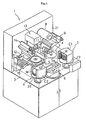
- Fig. 1 is a perspective view showing an overall construction of a protective tape applying and cutting apparatus.
- the protective tape applying and cutting apparatus 1 in this embodiment includes a base 2, and a wafer feeder 3 and a wafer collector 4 arranged on front regions of the base 2.
- the wafer feeder 3 receives a cassette C1 storing semiconductor wafers (hereinafter simply called "wafers") W which are an example of workpieces.
- the wafer collector 4 collects processed wafers W' having protective tape T, which is an example of adhesive tape, applied and trimmed to front surfaces thereof.
- Disposed between the wafer feeder 2 and wafer collector 3 is a wafer transport mechanism 6 having a robot arm 5.
- An alignment stage 7 is disposed in an inward right-hand position on the base 2, and a tape server 8 is disposed thereabove for feeding the protective tape T toward a wafer W.
- a separator collector 9 is disposed obliquely rightward below the tape server 8 for collecting only a separator s from the protective tape T with the separator fed from the tape server.
- To the left of the alignment stage 7 are a chuck table 10 for receiving and suction-supporting a wafer W, a tape applying unit 11 for applying the protective tape T to the wafer W held by the chuck table 10, and a tape separating unit 12 for separating unwanted tape T' after being applied to the wafer W and cut.
- a tape cutting mechanism 13 is disposed above for cutting off the protective tape T along the contour of wafer W.
- a tape collector 14 is disposed in a left-hand position above the base 2 for taking up and collecting the unwanted tape T' separated by the tape separator 12.
- static eliminators 15 are arranged opposite each other across the chuck table 10 for eliminating static electricity from the protective tape T before application to the wafer W and from the unwanted tape T' before collection.
- the wafer feeder 3 includes a vertically movable cassette table 17.
- the cassette table 17 is constructed to receive thereon a cassette C1 having wafers W stored in multiple stages therein with patterned surfaces facing upward.
- the robot arm 5 of the wafer transport mechanism 6 is constructed horizontally extendible and retractable as well as swivelable as a unit.
- the robot arm 5 has a horseshoe-shaped wafer holder 5a of the vacuum suction type attached to a distal end thereof.
- the wafer holder 5a is inserted into a space between wafers W stored in multiple stages in the cassette C1, sucks one of the wafers W by the back surface thereof, takes the wafer W out of the cassette C1, and transports the wafer W to the alignment stage 7, chuck table 10 and wafer collector 4 in the stated order.
- the wafer holder 5a is not limited to the above configuration, but may be in any form as long as it is capable of holding a wafer W in a way to avoid deflection that would hamper the suction holding.
- the wafer holder may have approximately the shape of wafer W for covering the entire surface of wafer W for suction.
- the alignment stage 7 receives the wafer W from the wafer transport mechanism 6, and adjusts position of the wafer W based on an orientation flat or notch formed peripherally thereof.
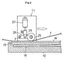
- the chuck table 10 suction-supports the wafer W received as adjusted to a predetermined position from the wafer transport mechanism 6, and has a heater 18 mounted therein as shown in Fig. 2. Further, the chuck table 10 has a cutter raceway groove 19 formed in an upper surface thereof for guiding a cutter 33 of the tape cutting mechanism 13, described hereinafter, to circle along the contour of wafer W to cut the protective tape.
- the chuck table 10 corresponds to the holding device and the heater 18 to the heating device of this invention.
- the tape server 8 guides the protective tape T with separator unwound from a tape bobbin 22 supported by a vertical wall 21 of an apparatus body to guide rollers 23, and guides the protective tape T stripped of the separator s to the tape applying unit 11. An appropriate rotational resistance is applied to the tape bobbin 22 to avoid excessive tape delivery.
- the tape server 8 corresponds to the tape feeding device of this invention.
- the separator collector 9 includes a collecting bobbin 24 supported by the vertical wall 21 of the apparatus body for taking up the separator s separated from the protective tape T.
- the collecting bobbin 24 is rotatable in a take-up direction by a drive mechanism, not shown, on the back of the vertical wall.
- the tape applying unit 11 is horizontally reciprocable right and left by a slide guide mechanism and a screw feed type drive mechanism, not shown, on the back of the vertical wall 21.
- the tape applying unit 11 includes a swing arm 26 attached to a front surface thereof to be vertically swingable about an axis y.
- the swing arm 26 has an applicator roller 25 acting as an applicator member attached to a free end thereof in a frontally extending cantilever fashion.
- the tape applying unit 11 corresponds to the applying device of this invention.
- the swing arm 26 is swingable up and down by an air cylinder 27.
- An electromagnetic vibration generating mechanism 28 is interposed between the air cylinder 27 and swing arms 26. This vibration generating mechanism 28 is constructed, when energized, to vibrate the applicator roller 25 vertically.
- the vibration generating mechanism 28 corresponds to the first vibration generating device of this invention.
- the tape separating unit 12 includes a separator roller 30 supported in a frontally extending cantilever fashion.
- the tape separating unit 12 is horizontally reciprocable right and left by a slide guide mechanism and a screw feed type drive mechanism, not shown, on the back of the vertical wall 21.
- the tape collector 14 includes a collecting bobbin 31 supported by the vertical wall 21 of the apparatus body for taking up unwanted tape T'.
- the collecting bobbin 31 is rotatable in a take-up direction by a drive mechanism, not shown, on the back of the vertical wall.
- the wafer collector 4 includes a vertically movable cassette table 32.
- the cassette table 32 is constructed to receive thereon a cassette C2 for storing, in multiple stages therein, processed wafers W' with the protective tape T applied thereto and unwanted tape cut off.
- the cassette table 17 of the wafer feeder When the cassette C1 containing wafers W in multiple stages is placed on the cassette table 17 of the wafer feeder, the cassette table 17 is moved vertically and stopped at a height for an intended wafer W to be fetched by the robot arm 5.
- the wafer transport mechanism 6 swivels to insert the wafer holder 5a of the robot arm 5 into a space between the wafers W in the cassette C1.
- the robot arm 5, with the wafer holder 5a takes out the wafer W while suction-supporting the back surface (lower surface) thereof, and transfers the wafer W to the alignment stage 7.
- the wafer W placed on the alignment stage 7 is positionally adjusted by using the orientation flat.
- the positionally adjusted wafer W is held by suction again by the robot arm 5 to be transferred to the chuck table 10.
- the wafer W placed on the chuck table 10 is suction-supported after a positional adjustment to have the center thereof registered with the center of the chuck table 10.
- the tape applying unit 11 and tape separating unit 12 are on standby in leftward initial positions, and the cutter 33 of the tape cutting mechanism 13 in an upper initial position.
- the applicator roller 25 of the tape applying unit 11 is lowered and rolls on the wafer W in a direction opposite to a tape running direction (from left to right in Fig. 4) while the applicator roller 25 presses down the protective tape T.
- the protective tape T is uniformly applied over the entire surface of wafer W.
- the applicator roller 25 is raised when the tape applying unit 11 reaches a terminal position.
- the vibration generating mechanism 28 is energized to vibrate the entire applicator roller 25 vertically, whereby the protective tape T follows minute irregularities on the wafer surface to be applied thereto reliably.
- the vibration frequency of the vibration generating mechanism 28 is variable in a range of 300 to 30,000 times/minute, and is preferably about 10,000 times/minute. While the slower traveling speed at this time of the applicator roller 25 provides the higher application performance, about 5mm/second is practical, considering operating efficiency.
- the vertical vibrational amplitude of the applicator roller 25 is set and varied according to the thickness of the protective tape, the level difference in irregularities of wafer W, and so on.
- the tape cutting mechanism 13 is lowered and, as shown in Fig. 5, the cutter 33 standing by in the upper position is lowered to a predetermined operative position piercing the protective tape T and lowered to and stopped at a predetermined height.
- the cutter lowered to the predetermined height is revolved about a vertical axis X to cut the protective tape T along the wafer contour.
- a predetermined tension is applied to the protective tape T by the tape applying unit 11 and tape separating unit 12.
- the cutter 33 is raised to the original standby position.
- the tape separating unit 12 while moving over the wafer W in the direction opposite to the tape running direction, takes up and separates the unwanted tape T' remaining uncut on the wafer W.
- the tape separating unit 12 When the tape separating unit 12 reaches a separating operation ending position, the tape separating unit 12 and tape applying unit 11 move in the tape running direction to return to the initial positions. At this time, the unwanted tape T' is wound on the collecting bobbin 31, and the protective tape T is drawn in a fixed amount from the tape server 8.
- the protective tape T is applied to the wafer W while the vibration generating mechanism 28 applies vibration to the applicator roller 25. This causes the adhesive of the protective tape to fill efficiently the level differences of fine irregularities of the pattern on the surface of wafer W without forcibly deforming the protective tape itself.
- the protective tape T may be applied to the wafer W reliably with no gap formed between wafer W and protective tape T.
- the protective tape may also be applied to the wafer W, with the surface of the protective tape maintained in a substantially planar state.
- the adhesive of the protective tape is heated and softened. The adhesive is thereby allowed to fill the level differences on the wafer W with ease.
Landscapes
- Engineering & Computer Science (AREA)
- Manufacturing & Machinery (AREA)
- Mechanical Engineering (AREA)
- Container, Conveyance, Adherence, Positioning, Of Wafer (AREA)
- Mechanical Treatment Of Semiconductor (AREA)
- Adhesive Tapes (AREA)
- Lead Frames For Integrated Circuits (AREA)
- Adhesive Tape Dispensing Devices (AREA)
- Coating Apparatus (AREA)
- Application Of Or Painting With Fluid Materials (AREA)
Abstract
Description
Claims (20)
- An adhesive tape applying method for placing an applicator member in contact with a surface of adhesive tape and applying the adhesive tape to a surface of a workpiece, said method comprising:a step of applying said adhesive tape to said workpiece while vibrating said adhesive tape.
- An adhesive tape applying method as defined in claim 1, wherein vibration is applied to said applicator member.
- An adhesive tape applying method as defined in claim 1, wherein vibration is applied to holding means for receiving and holding said workpiece.
- An adhesive tape applying method as defined in claim 1, further comprising:a step of applying said adhesive tape to said workpiece while heating said adhesive tape.
- An adhesive tape applying method as defined in claim 4, wherein said adhesive tape is heated by heating holding means.
- An adhesive tape applying method as defined in claim 1, wherein said applicator member is one or both of an applicator roller and an applicator edge member.
- An adhesive tape applying method as defined in claim 1, wherein said adhesive tape is in strip form.
- An adhesive tape applying method as defined in claim 1, wherein said adhesive tape is in label form shaped substantially to a shape of said workpiece beforehand.
- An adhesive tape applying method as defined in claim 1, wherein said workpiece is a semiconductor wafer.
- An adhesive tape applying apparatus for applying adhesive tape to a surface of a workpiece, comprising:holding means for receiving and holding said workpiece;tape feed means for feeding the adhesive tape toward the workpiece held by said holding means;applying means for placing an applicator member in contact with a surface of the adhesive tape and applying the adhesive tape to a surface of the workpiece; andfirst vibration generating means for vibrating said applying means.
- An adhesive tape applying apparatus as defined in claim 10, further comprising heating means for heating said holding means.
- An adhesive tape applying apparatus as defined in claim 10, further comprising cutting means for cutting the adhesive tape applied to said workpiece, substantially to a shape of said workpiece.
- An adhesive tape applying apparatus as defined in claim 10, wherein said first vibration generating means is electromagnetically operable.
- An adhesive tape applying apparatus as defined in claim 10, wherein said first vibration generating means is constructed for rotating an eccentric weight.
- An adhesive tape applying apparatus as defined in claim 10, further comprising second vibration generating means for vibrating said holding means.
- An adhesive tape applying apparatus as defined in claim 15, wherein said second vibration generating means is electromagnetically operable.
- An adhesive tape applying apparatus as defined in claim 15, wherein said second vibration generating means is constructed for rotating an eccentric weight.
- An adhesive tape applying apparatus as defined in claim 10, wherein said adhesive tape is in strip form.
- An adhesive tape applying apparatus as defined in claim 10, wherein said adhesive tape is in label form shaped substantially to a shape of said workpiece beforehand.
- An adhesive tape applying apparatus as defined in claim 10, wherein said workpiece is a semiconductor wafer.
Applications Claiming Priority (2)
| Application Number | Priority Date | Filing Date | Title |
|---|---|---|---|
| JP2003009652 | 2003-01-17 | ||
| JP2003009652A JP4187065B2 (en) | 2003-01-17 | 2003-01-17 | Adhesive tape application method and apparatus |
Publications (2)
| Publication Number | Publication Date |
|---|---|
| EP1439049A2 true EP1439049A2 (en) | 2004-07-21 |
| EP1439049A3 EP1439049A3 (en) | 2005-03-09 |
Family
ID=32588563
Family Applications (1)
| Application Number | Title | Priority Date | Filing Date |
|---|---|---|---|
| EP03028839A Withdrawn EP1439049A3 (en) | 2003-01-17 | 2003-12-16 | Adhesive tape applying method and apparatus |
Country Status (6)
| Country | Link |
|---|---|
| US (1) | US7135081B2 (en) |
| EP (1) | EP1439049A3 (en) |
| JP (1) | JP4187065B2 (en) |
| KR (1) | KR101055876B1 (en) |
| CN (1) | CN100377309C (en) |
| TW (1) | TWI311341B (en) |
Cited By (1)
| Publication number | Priority date | Publication date | Assignee | Title |
|---|---|---|---|---|
| CN103171789A (en) * | 2013-03-19 | 2013-06-26 | 华爵集团有限公司 | Door surface automatic film laminating machine |
Families Citing this family (29)
| Publication number | Priority date | Publication date | Assignee | Title |
|---|---|---|---|---|
| KR20050083322A (en) * | 2004-02-23 | 2005-08-26 | 삼성테크윈 주식회사 | Lead frame for semiconductor package and the fabrication method thereof |
| JP2006013073A (en) * | 2004-06-24 | 2006-01-12 | Sharp Corp | Bonding apparatus, bonding method, and semiconductor device manufacturing method |
| KR100725289B1 (en) * | 2005-03-17 | 2007-06-07 | 엘에스전선 주식회사 | Adhesive tape manufacturing apparatus for semiconductor manufacturing and manufacturing method thereof |
| JP4326519B2 (en) * | 2005-03-31 | 2009-09-09 | 日東電工株式会社 | Protective tape peeling method and apparatus using the same |
| JP4795743B2 (en) * | 2005-05-19 | 2011-10-19 | リンテック株式会社 | Pasting device |
| JP4795772B2 (en) * | 2005-10-24 | 2011-10-19 | リンテック株式会社 | Sheet cutting table and sheet sticking apparatus |
| JP2007214357A (en) * | 2006-02-09 | 2007-08-23 | Nitto Denko Corp | Work sticking support method and work sticking support apparatus using the same |
| JP4360684B2 (en) * | 2006-02-22 | 2009-11-11 | 日東電工株式会社 | Adhesive tape pasting method for semiconductor wafer and apparatus using the same |
| JP4286261B2 (en) * | 2006-02-22 | 2009-06-24 | 日東電工株式会社 | Adhesive tape pasting method for semiconductor wafer and apparatus using the same |
| JP5259978B2 (en) * | 2006-10-04 | 2013-08-07 | ローム株式会社 | Manufacturing method of semiconductor device |
| JP4746003B2 (en) * | 2007-05-07 | 2011-08-10 | リンテック株式会社 | Transfer device and transfer method |
| JP5010493B2 (en) * | 2008-02-05 | 2012-08-29 | ソニーケミカル&インフォメーションデバイス株式会社 | Transfer method of adhesive film |
| JP5551387B2 (en) * | 2009-07-03 | 2014-07-16 | リンテック株式会社 | Sheet sticking device and sticking method |
| JP5497534B2 (en) * | 2010-05-21 | 2014-05-21 | 株式会社ディスコ | Tape sticking device |
| KR101028789B1 (en) * | 2010-07-06 | 2011-04-11 | 주식회사 아레스 | Ring taping device |
| JP5054169B2 (en) * | 2010-08-06 | 2012-10-24 | リンテック株式会社 | Sheet cutting table |
| JP6058407B2 (en) * | 2013-01-23 | 2017-01-11 | 株式会社ディスコ | roller |
| KR101668188B1 (en) * | 2015-04-08 | 2016-10-28 | 조상희 | processing work table |
| JP6706746B2 (en) * | 2015-12-16 | 2020-06-10 | 株式会社タカトリ | Adhesive sheet pasting device and pasting method |
| KR101694498B1 (en) | 2016-10-07 | 2017-01-10 | 조상희 | Sofa band fixing device |
| CN106892156B (en) * | 2017-04-07 | 2022-10-25 | 位新喜 | Veneer tape machine |
| CN107335293A (en) * | 2017-07-11 | 2017-11-10 | 浙江宇邦滤材科技有限公司 | A kind of laminator of filter bag |
| KR101855049B1 (en) | 2017-12-01 | 2018-05-04 | 강병욱 | Method for manufacturing furniture |
| CN108163258B (en) * | 2017-12-29 | 2019-09-03 | 重庆翰邦汽车配件有限公司 | Foamed board film covering device |
| KR102503562B1 (en) * | 2020-04-07 | 2023-02-24 | 주식회사제이에스텍 | Apparatus for progressing web used in making electrode of secondary battery |
| CN111606121B (en) * | 2020-06-23 | 2024-11-01 | 上海新安汽车隔音毡有限公司 | Rated pressure compression roller device |
| CN112319910B (en) * | 2020-11-25 | 2025-01-24 | 深圳市锐欧光学股份有限公司 | Lens film laminating jig, film laminating jig and lens film laminating system |
| CN113401403B (en) * | 2021-06-30 | 2022-06-17 | 博锲思智能装备(青岛)有限公司 | Automatic edge bonding machine for plates |
| CA3224100A1 (en) * | 2022-10-28 | 2024-04-28 | Hiromoto Ito | Tape material applicator and computer program |
Family Cites Families (10)
| Publication number | Priority date | Publication date | Assignee | Title |
|---|---|---|---|---|
| US3630808A (en) * | 1967-05-10 | 1971-12-28 | Shinjiro Yasui | Apparatus for joining sheet materials by vibrating plates |
| GB1220621A (en) * | 1968-05-06 | 1971-01-27 | Shell Int Research | Method and apparatus for laminating sheets |
| US3925126A (en) * | 1973-07-05 | 1975-12-09 | Heller William C Jun | Vibratory book binding method |
| US4239580A (en) * | 1978-07-31 | 1980-12-16 | Ives Frank E | Impregnated fabric applicator with vibrating applicator rolls |
| US4544426A (en) * | 1983-10-24 | 1985-10-01 | Shaw Industries Ltd. | Method and apparatus for applying a coating material to a pipe |
| US4696714A (en) * | 1986-01-22 | 1987-09-29 | Theodore Voorhees | Foil applicator |
| JPH01143211A (en) * | 1987-11-27 | 1989-06-05 | Takatori Haitetsuku:Kk | Sticking and cutting of protective tape for wafer and device therefor |
| JPH10129614A (en) * | 1996-10-28 | 1998-05-19 | Nichiban Co Ltd | Binding machine |
| JP2000073031A (en) * | 1998-08-31 | 2000-03-07 | Mitsui High Tec Inc | Method and device for attaching insulating tape |
| JP4482286B2 (en) * | 2003-03-31 | 2010-06-16 | シャープ株式会社 | Illumination device and display device including the same |
-
2003
- 2003-01-17 JP JP2003009652A patent/JP4187065B2/en not_active Expired - Fee Related
- 2003-12-10 US US10/730,999 patent/US7135081B2/en not_active Expired - Fee Related
- 2003-12-16 EP EP03028839A patent/EP1439049A3/en not_active Withdrawn
-
2004
- 2004-01-13 KR KR1020040002196A patent/KR101055876B1/en not_active Expired - Fee Related
- 2004-01-16 CN CNB2004100027424A patent/CN100377309C/en not_active Expired - Fee Related
- 2004-01-16 TW TW093101114A patent/TWI311341B/en not_active IP Right Cessation
Cited By (1)
| Publication number | Priority date | Publication date | Assignee | Title |
|---|---|---|---|---|
| CN103171789A (en) * | 2013-03-19 | 2013-06-26 | 华爵集团有限公司 | Door surface automatic film laminating machine |
Also Published As
| Publication number | Publication date |
|---|---|
| EP1439049A3 (en) | 2005-03-09 |
| JP2004221469A (en) | 2004-08-05 |
| CN1518071A (en) | 2004-08-04 |
| TW200503090A (en) | 2005-01-16 |
| US7135081B2 (en) | 2006-11-14 |
| TWI311341B (en) | 2009-06-21 |
| KR20040067896A (en) | 2004-07-30 |
| US20040140039A1 (en) | 2004-07-22 |
| KR101055876B1 (en) | 2011-08-09 |
| CN100377309C (en) | 2008-03-26 |
| JP4187065B2 (en) | 2008-11-26 |
Similar Documents
| Publication | Publication Date | Title |
|---|---|---|
| US7135081B2 (en) | Adhesive tape applying method and apparatus | |
| US20100038009A1 (en) | Method and apparatus for joining protective tape to semiconductor wafer | |
| CN100459055C (en) | Protective tape attaching method and device thereof, protective tape detaching method and device thereof | |
| US6919284B2 (en) | Protective tape applying method and apparatus, and protective tape separating method | |
| JP2004047823A (en) | Dicing tape sticking device and back grinding / dicing tape sticking system | |
| JP4136890B2 (en) | Method and apparatus for cutting protective tape | |
| JP2000068293A (en) | Wafer transfer device | |
| JP2007266352A (en) | Wafer processing method | |
| KR20030063179A (en) | Method of cutting a protective tape and protective tape applying apparatus using the same method | |
| US6332268B1 (en) | Method and apparatus for packaging IC chip, and tape-shaped carrier to be used therefor | |
| JP2004047976A (en) | Method and device for attaching protective tape | |
| US7118645B2 (en) | Method and apparatus for joining protective tape to semiconductor wafer | |
| KR102952110B1 (en) | Processing apparatus | |
| US7264998B2 (en) | Method of removing unnecessary matter from semiconductor wafer, and apparatus using the same | |
| JP4475772B2 (en) | Protective tape application method and protective tape application device | |
| JP2022041495A (en) | Protective member forming device | |
| JP2005260154A (en) | Method of manufacturing chip | |
| JP4326363B2 (en) | Adhesive sheet pasting method and apparatus using the same | |
| JP2013232583A (en) | Protection tape cutting method and protection tape cutting device of semiconductor wafer | |
| JP4060641B2 (en) | Tape peeling method | |
| CN100401480C (en) | Method and apparatus for joining adhesive tape | |
| JP2004079768A (en) | Pasting device | |
| JP7401904B2 (en) | Apparatus and method for applying adhesive tape to a board | |
| JP4632632B2 (en) | Adhesive tape application method and apparatus | |
| TW201721790A (en) | Adhesive tape attachment method and adhesive tape attachment device |
Legal Events
| Date | Code | Title | Description |
|---|---|---|---|
| PUAI | Public reference made under article 153(3) epc to a published international application that has entered the european phase |
Free format text: ORIGINAL CODE: 0009012 |
|
| AK | Designated contracting states |
Kind code of ref document: A2 Designated state(s): AT BE BG CH CY CZ DE DK EE ES FI FR GB GR HU IE IT LI LU MC NL PT RO SE SI SK TR |
|
| AX | Request for extension of the european patent |
Extension state: AL LT LV MK |
|
| PUAL | Search report despatched |
Free format text: ORIGINAL CODE: 0009013 |
|
| AK | Designated contracting states |
Kind code of ref document: A3 Designated state(s): AT BE BG CH CY CZ DE DK EE ES FI FR GB GR HU IE IT LI LU MC NL PT RO SE SI SK TR |
|
| AX | Request for extension of the european patent |
Extension state: AL LT LV MK |
|
| RIC1 | Information provided on ipc code assigned before grant |
Ipc: 7H 01L 21/00 B Ipc: 7B 29C 63/02 A |
|
| AKX | Designation fees paid |
Designated state(s): AT BE BG CH CY CZ DE DK EE ES FI FR GB GR HU IE IT LI LU MC NL PT RO SE SI SK TR |
|
| STAA | Information on the status of an ep patent application or granted ep patent |
Free format text: STATUS: THE APPLICATION IS DEEMED TO BE WITHDRAWN |
|
| 18D | Application deemed to be withdrawn |
Effective date: 20050910 |