EP1437768A1 - Plasma cleaning gas and plasma cleaning method - Google Patents
Plasma cleaning gas and plasma cleaning method Download PDFInfo
- Publication number
- EP1437768A1 EP1437768A1 EP02758871A EP02758871A EP1437768A1 EP 1437768 A1 EP1437768 A1 EP 1437768A1 EP 02758871 A EP02758871 A EP 02758871A EP 02758871 A EP02758871 A EP 02758871A EP 1437768 A1 EP1437768 A1 EP 1437768A1
- Authority
- EP
- European Patent Office
- Prior art keywords
- plasma
- gas
- cleaning
- fluorine
- cvd
- Prior art date
- Legal status (The legal status is an assumption and is not a legal conclusion. Google has not performed a legal analysis and makes no representation as to the accuracy of the status listed.)
- Granted
Links
Images
Classifications
-
- C—CHEMISTRY; METALLURGY
- C23—COATING METALLIC MATERIAL; COATING MATERIAL WITH METALLIC MATERIAL; CHEMICAL SURFACE TREATMENT; DIFFUSION TREATMENT OF METALLIC MATERIAL; COATING BY VACUUM EVAPORATION, BY SPUTTERING, BY ION IMPLANTATION OR BY CHEMICAL VAPOUR DEPOSITION, IN GENERAL; INHIBITING CORROSION OF METALLIC MATERIAL OR INCRUSTATION IN GENERAL
- C23C—COATING METALLIC MATERIAL; COATING MATERIAL WITH METALLIC MATERIAL; SURFACE TREATMENT OF METALLIC MATERIAL BY DIFFUSION INTO THE SURFACE, BY CHEMICAL CONVERSION OR SUBSTITUTION; COATING BY VACUUM EVAPORATION, BY SPUTTERING, BY ION IMPLANTATION OR BY CHEMICAL VAPOUR DEPOSITION, IN GENERAL
- C23C16/00—Chemical coating by decomposition of gaseous compounds, without leaving reaction products of surface material in the coating, i.e. chemical vapour deposition [CVD] processes
- C23C16/44—Chemical coating by decomposition of gaseous compounds, without leaving reaction products of surface material in the coating, i.e. chemical vapour deposition [CVD] processes characterised by the method of coating
- C23C16/4401—Means for minimising impurities, e.g. dust, moisture or residual gas, in the reaction chamber
- C23C16/4405—Cleaning of reactor or parts inside the reactor by using reactive gases
-
- B—PERFORMING OPERATIONS; TRANSPORTING
- B08—CLEANING
- B08B—CLEANING IN GENERAL; PREVENTION OF FOULING IN GENERAL
- B08B7/00—Cleaning by methods not provided for in a single other subclass or a single group in this subclass
- B08B7/0035—Cleaning by methods not provided for in a single other subclass or a single group in this subclass by radiant energy, e.g. UV, laser, light beam or the like
-
- H—ELECTRICITY
- H10—SEMICONDUCTOR DEVICES; ELECTRIC SOLID-STATE DEVICES NOT OTHERWISE PROVIDED FOR
- H10P—GENERIC PROCESSES OR APPARATUS FOR THE MANUFACTURE OR TREATMENT OF DEVICES COVERED BY CLASS H10
- H10P50/00—Etching of wafers, substrates or parts of devices
- H10P50/20—Dry etching; Plasma etching; Reactive-ion etching
- H10P50/24—Dry etching; Plasma etching; Reactive-ion etching of semiconductor materials
- H10P50/242—Dry etching; Plasma etching; Reactive-ion etching of semiconductor materials of Group IV materials
-
- Y—GENERAL TAGGING OF NEW TECHNOLOGICAL DEVELOPMENTS; GENERAL TAGGING OF CROSS-SECTIONAL TECHNOLOGIES SPANNING OVER SEVERAL SECTIONS OF THE IPC; TECHNICAL SUBJECTS COVERED BY FORMER USPC CROSS-REFERENCE ART COLLECTIONS [XRACs] AND DIGESTS
- Y10—TECHNICAL SUBJECTS COVERED BY FORMER USPC
- Y10S—TECHNICAL SUBJECTS COVERED BY FORMER USPC CROSS-REFERENCE ART COLLECTIONS [XRACs] AND DIGESTS
- Y10S438/00—Semiconductor device manufacturing: process
- Y10S438/905—Cleaning of reaction chamber
Definitions
- the present invention relates to plasma cleaning gases for CVD chambers, which gases are used in order to remove deposits on the inner wall surface or other surfaces of CVD chambers during film forming treatment in plasma CVD (Chemical Vapor Deposition) apparatus in which the film forming treatment with silicon oxide, silicon nitride etc. is conducted on the substrate surfaces for semiconductors etc., and further relates to processes for plasma cleaning of the CVD chambers.
- plasma CVD Chemical Vapor Deposition
- the term "uniformity of cleaning" used herein is an indication of stability of generated plasma and is evaluated in the following manner, as also described in the examples. A wafer previously deposited with SiO 2 film by CVD is used as a sample and is placed on the lower electrode, and then the etching rate is measured. The evaluation of the uniformity of the etching rate on the inside of the wafer surface is taken as a typical evaluation of uniformity of cleaning. This property is evaluated likewise hereinafter.
- etching rate used herein is an indication of evaluating the rate of cleaning and is evaluated by measuring the rate of etching a SiO 2 thin film on a wafer as described in the examples. The etching rate is taken as a typical evaluation of cleaning. The property is evaluated likewise hereinafter.
- exhaust gases include the perfluoro compounds themselves which compounds are not decomposed even if plasma is generated.
- exhaust gases contain CF 4 , etc. which are generated as a by-product. So they induce an environmental problem of exhausting global warming gases.
- the gases inviting the greenhouse effect and global warming gas contained in the exhaust gases as described above are hardly absorbed or decomposed by abatement apparatus (water scrubber) which apparatus has conventionally been used mainly, so that a decomposition apparatus by chemical reactions including burning with high temperature and high energy is required.
- abatement apparatus water scrubber
- an additional gas such as oxygen, argon etc. is mixed with the cleaning gases.
- the etching rates tend to be increased.
- the cleaning gas concentrations are over constant concentrations, there are problems such as instability in plasma generation, slowdown or lowering of the etching rate, deterioration in uniformity of cleaning etc..
- using the cleaning gas in a concentration of 100% induces a more marked tendency toward instability in plasma generation, slowdown or lowering of the etching rate and deterioration in the uniformity of cleaning so that it has a problem such that it is lacking in practical use.
- the cleaning gases need to be diluted so as to have the peak concentration in the etching rate-cleaning gas concentration curve or a lower concentration than the peak concentration.
- the cleaning condition has been optimized by increasing the chamber pressure or increasing the gas flow rate in cleaning.
- the plasma generation becomes unstable, so that the uniformity of cleaning is deteriorated and efficient cleaning cannot be conducted.
- a remote plasma apparatus in which plasma is generated other than a process chamber of a CVD apparatus is required for securing a high decomposition rate which is one of the objects so that the cleaning efficiency is improved, contamination of undecomposed NF 3 into exhaust gases is avoided.
- the CVD apparatus provided with the remote plasma apparatus has a problem in that the apparatus is complicated and thereby the production cost is high.
- plasma cleaning gases which are used for chamber cleaning after the CVD process in producing semiconductors such as LSI, etc., and have a low greenhouse effect and a low global warming potential, excellent uniformity of cleaning even in diluting conditions or not, and also have an effective etching rate, and a process for plasma cleaning has been desired.
- the present inventors have earnestly studied for solving the above problems, and found that when a mixed gas of fluorine gas and a gas incapable of substantially reacting with fluorine in plasma is used, plasma can be generated stably without a remote plasma apparatus in wider conditions than the use of, for example, NF 3 and further the excellent etching rate can be provided without lowering of the etching rate.
- the present inventors further found that for example, as will be described in Examples 34 and 37, and Comparative Examples 30 and 31 of the present specification, in the case that the total gas flow rate is 1000 sccm, when the chamber pressure condition is changed from 250 Pa to a higher pressure of 400 Pa, in the use of a mixed gas containing 20% by volume of NF 3 , the uniformity of cleaning is decreased, but in the use of a mixed gas containing the same 20 % by volume of fluorine gas, the proper uniformity of cleaning can be secured.
- the present inventors found that when 100 % by volume of fluorine gas is generated by plasma and then is used as a cleaning gas, the extremely excellent etching rate can be attained without the use of a remote plasma apparatus, and also even in conditions that the total gas flow rate is about 1000 sccm and the chamber pressure is about 400 Pa, plasma can stably be generated and the proper uniformity of cleaning can be secured.
- the present invention is intended to solve the problems associated with the prior arts as described above, it is an object of the present invention to provide a plasma cleaning gas for CVD chambers which gas has excellent uniformity of cleaning and an effective etching rate in cleaning in the conditions that the total gas flow rate is about 1000 sccm and the chamber pressure is about 400 Pa under the dilution condition or under no dilution condition. It is a further object of the invention to provide a process for plasma cleaning CVD chambers.
- the first plasma cleaning gas for CVD chambers comprises 100 % by volume of fluorine gas capable of generating plasma by electric discharge and is used for cleaning silicon-containing deposits on the surface of a CVD chamber inner wall and the surfaces of members placed inside the CVD chamber after film forming treatment on a substrate by a plasma CVD apparatus.
- the first process of plasma cleaning for CVD chambers comprises cleaning silicon-containing deposits on the surface of a CVD chamber inner wall and the surfaces of members placed inside the CVD chamber by plasma generated from 100 % by volume of fluorine gas by electric discharge, after film forming treatment on a substrate in a plasma CVD apparatus.
- the silicon-containing deposits preferably comprise at least one selected from:
- the chamber pressure in the plasma CVD apparatus is preferably from 50 Pa to 1000 Pa, and the flow rate of fluorine gas introducing into a plasma generating part is preferably from 50 sccm to 1000 sccm in the cleaning.
- the plasma generation from the above-described fluorine gas is preferably conducted by electric discharge in a process chamber of the plasma CVD apparatus whereinto fluorine gas has been introduced.
- the second plasma cleaning gas for CVD chambers comprises fluorine gas capable of generating plasma by electric discharge and a gas substantially incapable of reacting with fluorine in plasma, and is used for cleaning silicon-containing deposits on the surface of a CVD chamber inner wall and the surfaces of members placed inside the CVD chamber after film forming treatment on a substrate by a plasma CVD apparatus.
- the concentration of the fluorine gas capable of generating plasma by electric discharge be more than 20 % by volume to less than 100 % by volume and the concentration of the gas substantially incapable of reacting with fluorine in plasma be more than 0 % by volume to not more than 80 % by volume provided that the total concentration of the fluorine gas capable of generating plasma by electric discharge and the gas substantially incapable of reacting with fluorine is 100 % by volume.
- the concentration of the fluorine gas capable of generating plasma by electric discharge be more than 30 % by volume to less than 100 % by volume and the concentration of the gas substantially incapable of reacting with fluorine in plasma be more than 0 % by volume to not more than 70 % by volume provided that the total concentration of the fluorine gas capable of generating plasma by electric discharge and the gas substantially incapable of reacting with fluorine in plasma is 100 % by volume.
- the gas substantially incapable of reacting with fluorine in plasma is preferably at least one selected from the group of nitrogen, oxygen, carbon dioxide, N 2 O, dried air, argon, helium and neon.
- the second process of plasma cleaning for CVD chambers comprises cleaning silicon-containing deposits on the surface of a CVD chamber inner wall and the surfaces of members placed inside the CVD chamber using a cleaning gas for plasma CVD chambers comprising fluorine gas capable of generating plasma by electric discharge and a gas substantially incapable of reacting with fluorine in plasma after film forming treatment on a substrate by means of a plasma CVD apparatus.
- a cleaning gas for plasma CVD chambers comprising fluorine gas capable of generating plasma by electric discharge and a gas substantially incapable of reacting with fluorine in plasma after film forming treatment on a substrate by means of a plasma CVD apparatus.
- the concentration of the fluorine gas capable of generating plasma by electric discharge be more than 20 % by volume to less than 100 % by volume and the concentration of the gas substantially incapable of reacting with fluorine in plasma be more than 0 % by volume to not more than 80 % by volume provided that the total concentration of the fluorine gas capable of generating plasma by electric discharge and the gas substantially incapable of reacting with fluorine is 100 % by volume.
- the pressure in the chamber is preferably from 50 Pa to 1000 Pa, and the flow rate of fluorine gas is preferably from 50 sccm to 1000 sccm in the cleaning.
- the plasma generation from fluorine gas is preferably conducted by electric discharge in a process chamber of the plasma CVD apparatus whereinto fluorine gas has been introduced.
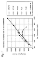
- Fig. 1 is a graph showing a relation between a gas concentration and an etching rate concerning the results of Examples 1 to 17 and Comparative Examples 1 to 13.
- the plasma cleaning gas for CVD chambers according to the first invention is used for cleaning silicon-containing deposits on the surface of a CVD chamber inner wall and the surfaces of members placed inside the CVD chamber after film forming treatment on a substrate by a plasma CVD apparatus.
- the cleaning gas comprises 100 % by volume of fluorine gas and generates plasma from fluorine gas by electric discharge to remove the silicon-containing deposits as described above.
- the first process of plasma cleaning for CVD chambers comprises cleaning, by plasma generated from 100 % by volume of fluorine gas by electric discharge, silicon-containing deposits on the surface of a CVD chamber inner wall and the surfaces of members placed inside the CVD chamber after film forming treatment on a substrate by means of a plasma CVD apparatus.
- plasma cleaning for CVD chambers means removing deposits on the surface of a chamber inner wall and the surfaces of members such as jigs, piping or other inside components placed in semiconductor producing apparatus, for example, CVD apparatus or the like after the CVD process in a production process of semiconductors such as LSI, etc.
- plasma generation used in the present specification means that plasma is generated by introducing fluorine gas or the mixed gas of fluorine gas and the gas substantially incapable of reacting with fluorine in plasma and electrically discharging at a plasma generating part (CVD chamber or remote plasma apparatus).
- the targeted compound of the CVD chamber cleaning with such 100 % by volume of fluorine gas may include the above described silicon-containing deposits on the surfaces of the inner wall of CVD chambers and jigs or the like of CVD apparatus in the CVD method, etc..
- the silicon-containing deposits comprise, for example, at least one selected from:
- the plasma generation from fluorine gas by electric discharge may be conducted in a remote chamber or in a process chamber of a plasma CVD apparatus whereinto fluorine gas is introduced without using the remote chamber.
- the cleaning treatment of deposits in the CVD chamber can be conducted efficiently for a short time, and also plasma can be stably generated. Further, the apparatus can be compacted so that it is practical as compared with the plasma generation in the remote chamber.
- the first cleaning gas of the invention comprises 100% by volume of fluorine gas and is used for plasma cleaning for CVD chambers.
- C 2 F 6 or NF 3 is used as a cleaning gas
- 100 % by volume of the gas is not used, and it is necessary to mix the gas with a diluting gas such as oxygen, argon, nitrogen etc. for use.
- a diluting gas such as oxygen, argon, nitrogen etc.
- the rise of the etching rate based on the concentration in the cleaning gas, in a constant total gas flow rate is slowed down and the etching rate is lowered finally.
- the total gas flow rate is 1000 sccm and the chamber pressure is about 400 Pa as described above, these gases cannot generate plasma stably.
- the uniformity of cleaning becomes worse.
- fluorine gas is used and the cleaning gas has a specific characteristic such that the etching rate is increased almost linearly with the increase of the concentration of fluorine gas in the condition that the total gas flow rate is constant. Even if the cleaning gas comprises 100% by volume of fluorine gas, the extremely excellent etching rate can be attained and also the uniformity of cleaning is extremely excellent.
- plasma can be stably generated, not only in the case that the chamber pressure is 150 Pa (flow rate 150 sccm) but also in the case that the chamber pressure is 250 Pa (flow rate 300 sccm) .
- the cleaning gas having the specific characteristic as above has not been found out previously so long as the present inventors have investigated.
- the chamber pressure is preferably from 50 Pa to 1000 Pa, more preferably from 150 Pa to 1000 Pa.
- the fluorine gas flow rate is preferably from 50 sccm to 1000 sccm, more preferably 150 to 1000 sccm.
- the excellent etching rate can be attained, and the stabilization of plasma generation and the uniformity of cleaning can be kept excellent.
- the chamber pressure is an inner pressure of a process chamber in a CVD apparatus and, in general, is automatically regulated by setting.
- the plasma cleaning gas for CVD chambers according to the second invention is used for cleaning silicon-containing deposits on the surface of a CVD chamber inner wall and the surfaces of members placed inside the CVD chamber after film forming treatment on a substrate by a plasma CVD apparatus.
- the plasma cleaning gas comprises fluorine gas capable of generating plasma by electric discharge and a gas substantially incapable of reacting with fluorine in plasma.
- the second process of plasma cleaning for CVD chambers comprises cleaning silicon-containing deposits on the surface of a CVD chamber inner wall and the surfaces of members placed inside the CVD chamber by plasma generated from fluorine gas by electric discharge using the plasma cleaning gas for CVD chambers composed of fluorine gas capable of generating plasma by electric discharge and the gas substantially incapable of reacting with fluorine in plasma, after film forming treatment on a substrate by means of a plasma CVD apparatus.
- fluorine contained in the gas substantially incapable of reacting with fluorine includes fluorine molecules, fluorine atoms, fluorine radicals, fluorine ions etc.
- the concentration of the fluorine gas capable of generating plasma by electric discharge is preferably more than 20 % by volume to less than 100 % by volume, and the concentration of the gas substantially incapable of reacting with fluorine in plasma is preferably more than 0 % by volume to not less than 80 % by volume.
- the sum of the concentration of the fluorine gas capable of generating plasma by electric discharge and the concentration of the gas substantially incapable of reacting with fluorine in plasma is 100 % by volume.
- the concentration of the fluorine gas capable of generating plasma by electric discharge is, further, preferably more than 30 % by volume to less than 100 % by volume, more preferably not less than 40 % by volume to less than 100 % by volume, and especially not less than 70 % by volume to less than 100 % by volume
- the concentration of the gas substantially incapable of reacting with fluorine in plasma is, further, preferably more than 0 % by volume to not more than 70 % by volume, more preferably more than 0 % by volume to less than 60 % by volume, and especially more than 0 % by volume to less than 30 % by volume.
- the excellent etching rate can be attained and the uniformity of cleaning is good even in the conditions that the total gas flow rate is about 1000 sccm and the chamber pressure is about 400 Pa. Further, plasma can be generated stably in the presence of fluorine gas.
- the etching rate has a specific characteristic such that the etching rate and the concentration of fluorine gas are increased almost linearly so that the etching rate is easily predictable from the fluorine gas concentration and it is effective in practical use.
- the concentration of fluorine gas for submitting to plasma treatment is preferably more than 20 % by volume, more preferably more than 30 % by volume. Particularly, it is preferably not more than 50 % by volume, so that the cleaning gas has a practicability maintainable etching rate and also, as a cleaning gas, excellent transportation property and storage stability, and simple handling. Furthermore, as described above, although this concentration range is a relatively low concentration range, the uniformity of cleaning is not deteriorated even if the chamber pressure is increased in order to increase the etching rate in this concentration range.
- the concentration of fluorine gas for submitting to plasma treatment is in a low range of 5 to 20 % by volume, the uniformity of cleaning is not deteriorated by increasing the chamber pressure in order to increase the etching rate.
- the gas substantially incapable of reacting with fluorine in plasma is preferably at least one selected from the group of nitrogen, oxygen, carbon dioxide, N 2 O, dried air, argon, helium and neon. Among them, it is more preferably at least one selected from the group of oxygen, carbon dioxide and dried air.
- the fluorine gas introduced in plasma generates fluorine radicals.
- the gas substantially incapable of reacting with the fluorine radicals, fluorine molecules, fluorine ions etc. the by-product generation can be depressed and the cleaning can be conducted efficiently.
- fluorine radicals can be generated stably at low cost.
- the chamber pressure is preferably from 50 Pa to 1000 Pa, more preferably 150 Pa to 1000 Pa.
- the fluorine gas flow rate is preferably from 50 sccm to 1000 sccm, more preferably 150 sccm to 1000 sccm.
- the excellent etching rate can be attained and also the stabilization of plasma generation and the uniformity of cleaning can be kept excellent.
- the plasma generation from fluorine gas by electric discharge may be conducted in a remote chamber or by introducing fluorine gas into a plasma CVD apparatus and generating plasma from fluorine gas in a process chamber of the CVD apparatus, without using the remote chamber.
- the cleaning treatment of deposits in the CVD chamber can be conducted efficiently for a short time, and also plasma can be stably generated similar to the first invention. Further, the apparatus can be compacted so that it is practical as compared with the plasma generation in the remote chamber.
- the cleaning rate for deposits, which should be removed was unequivocally evaluated by the etching rate of a SiO 2 thin film on a wafer.
- the method of measuring the etching rates of fluorine gas and diluted fluorine gas is shown below.
- a Si wafer previously deposited SiO 2 film thereon having a thickness of about 11000 ⁇ by the plasma CVD method was used as a sample and a parallel plate plasma enhanced CVD apparatus was used.
- the wafer as a sample was placed on a lower electrode of the parallel plate electrodes and etched.
- the etching rate was determined by accurately measuring the film thickness on nine fixed points of the sample before and after the etching with a spectroscopic reflectmeter film thickness measuring instrument and measuring the decrease in the film thickness.
- the uniformity of cleaning was determined from the maximum value and the minimum value of the etching rates on the nine fixed points with the following formula. [(maximum value - minimum value) / (maximum value + minimum value)] x 100 (%)
- NF 3 in the case that the added gas was argon, when the NF 3 concentration was not less than 50%, the uniformity of cleaning was largely deteriorated and when the NF 3 concentration was 60%, the lowering of the etching rate was observed. In the case that the added gas was nitrogen, when the NF 3 concentration was 40%, the uniformity of cleaning was largely deteriorated. It is presumed that the deterioration shows an indication such that plasma generated is biased and thereby plasma is not generated stably.
- fluorine gas is used as a cleaning gas
- silicon-containing deposits after CVD process can be cleaned at a high rate without using CF 4 , C 2 F 6 , SF 6 , NF 3 etc. which have a high global warming potential, and exhaust gas can be treated with conventional water scrubber. Therefore, the cleaning can be accomplished with exhausting a slight amount of exhaust gases having the greenhouse effect and the global warming effect.
- the mixed gas of fluorine gas and the gas incapable of substantially reacting with fluorine in plasma in specific amounts plasma can stably be generated even in the conditions that the total gas flow rate is about 1000 sccm and the chamber pressure is about 400 Pa. Additionally, the etching rate is not lowered and the excellent etching rate can be provided. Further, for example, even if the mixed gas has a low concentration of fluorine gas of 5 to 20 % by volume, the uniformity of cleaning can be ensured even in the conditions that the total gas flow rate and the chamber pressure are as described above. Further, the mixed gas having a low concentration of fluorine gas is simple in handleability.
- the cleaning gas has a fluorine gas concentration of 100% so that the device is not complicated and the cleaning gas is excellent in practicability.
Landscapes
- Chemical & Material Sciences (AREA)
- General Chemical & Material Sciences (AREA)
- Chemical Kinetics & Catalysis (AREA)
- Engineering & Computer Science (AREA)
- Materials Engineering (AREA)
- Mechanical Engineering (AREA)
- Metallurgy (AREA)
- Organic Chemistry (AREA)
- Physics & Mathematics (AREA)
- Optics & Photonics (AREA)
- Drying Of Semiconductors (AREA)
- Chemical Vapour Deposition (AREA)
Abstract
Description
| Total gas flow rate | 300 sccm |
| Chamber pressure | 250 Pa |
| Electrode temperature | 300°C |
| RF electric power | 750 W |
| Distance between electrodes | 50 mm |
| Electric discharge time | 30 sec |
| Ex.1 | Ex.2 | Ex.3 | Ex.4 | Ex.5 | ||
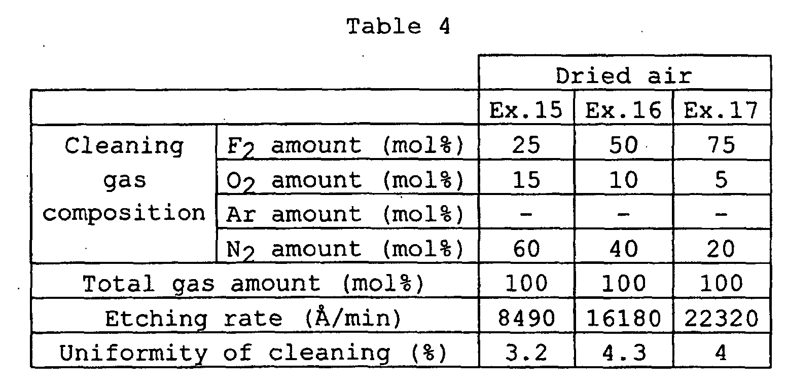
| Cleaning gas composition | F2 amount (mol%) | 10 | 25 | 50 | 75 | 100 |
| O2 amount (mol%) | 90 | 75 | 50 | 25 | 0 | |
| Ar amount (mol%) | - | - | - | - | - | |
| N2 amount (mol%) | - | - | - | - | - | |
| Total gas amount (mol%) | 100 | 100 | 100 | 100 | 100 | |
| Etching rate (Å/min) | 3460 | 8190 | 15960 | 21800 | 29420 | |
| Uniformity of cleaning (%) | 3 | 3.2 | 4 | 3.9 | 4.1 |
| Ex.6 | Ex.7 | Ex.8 | Ex.9 | Ex.10 | Ex.11 | ||
| Cleaning gas composition | F2 amount (mol%) | 5 | 10 | 20 | 25 | 50 | 75 |
| O2 amount (mol%) | - | - | - | - | - | - | |
| Ar amount (mol%) | 95 | 90 | 80 | 75 | 50 | 25 | |
| N2 amount (mol%) | - | - | - | - | - | - | |
| Total gas amount (mol%) | 100 | 100 | 100 | 100 | 100 | 100 | |
| Etching rate (Å/min) | 2190 | 4230 | 7090 | 8800 | 16440 | 22240 | |
| Uniformity of cleaning (%) | 4.2 | 3.6 | 3.3 | 3.9 | 3.4 | 4.5 |
| Ex.12 | Ex.13 | Ex.14 | ||
| Cleaning gas composition | F2 amount (mol%) | 25 | 50 | 75 |
| O2 amount (mol%) | - | - | - | |
| Ar amount (mol%) | - | - | - | |
| N2 amount mol% | 75 | 50 | 25 | |
| Total gas amount (mol%) | 100 | 100 | 100 | |
| Etching rate (Å/min) | 8570 | 16230 | 22450 | |
| Uniformity of cleaning (%) | 3.2 | 6.2 | 4.2 |
| Comparative Example | ||||||||
| 1 | 2 | 3 | 4 | 5 | 6 | 7 | ||
| Cleaning gas composition | C2F6 amount (mol%) | 20 | 40 | 45 | 50 | 55 | 60 | 70 |
| O2 amount (mol%) | 80 | 60 | 55 | 50 | 45 | 40 | 30 | |
| NF3 amount (mol%) | - | - | - | - | - | - | - | |
| Ar amount (mol%) | - | - | - | - | - | - | - | |
| Total gas amount (mol%) | 100 | 100 | 100 | 100 | 100 | 100 | 100 | |
| Etching rate (Å/min) | 7810 | 11810 | 12270 | 12410 | 12140 | 11140 | 7590 | |
| Uniformity of cleaning (%) | 4.7 | 4.3 | 4 | 3.5 | 4 | 3.1 | 1.9 |
| Comparative Example | |||||||
| 8 | 9 | 10 | 11 | 12 | 13 | ||
| Cleaning gas composition | C2F6 amount (mol%) | - | - | - | - | - | - |
| O2 amount (mol%) | - | - | - | - | - | - | |
| NF3 amount (mol%) | 10 | 20 | 30 | 40 | 50 | 60 | |
| Ar amount (mol%) | 90 | 80 | 70 | 60 | 50 | 40 | |
| Total gas amount (mol%) | 100 | 100 | 100 | 100 | 100 | 100 | |
| Etching rate (Å/min) | 5070 | 9080 | 12510 | 15310 | 17180 | 16080 | |
| Uniformity of cleaning (%) | 3.3 | 3.4 | 3.4 | 4.1 | 24 | 36 |
| Comparative Example | ||||
| 14 | 15 | 16 | ||
| Cleaning gas composition | C2F6 amount (mol%) | - | - | - |
| O2 amount (mol%) | - | - | - | |
| NF3 amount (mol%) | 10 | 30 | 40 | |
| N2 amount (mol%) | 90 | 70 | 60 | |
| Total gas amount (mol%) | 100 | 100 | 100 | |
| Etching rate (Å/min) | 4872 | 12298 | 14316 | |
| Uniformity of cleaning (%) | 3.2 | 5.4 | 31.5 |
| Electrode temperature | 300°C |
| RF electric power | 750W |
| Distance between electrodes | 50 mm |
| Electric discharge time | 30 sec |
| Ex 18 | Ex 19 | Ex 20 | Ex 21 | ||
| Total gas flow rate (sccm) | 300 | 300 | 300 | 300 | |
| Chamber pressure (Pa) | 250 | 250 | 250 | 150 | |
| Cleaning gas composition | F2 amount (mol%) | 5 | 10 | 20 | 5 |
| Ar amount (mol%) | 95 | 90 | 80 | 95 | |
| Total gas amount (mol%) | 100 | 100 | 100 | 100 | |
| Etching rate (Å/min) | 2192 | 4234 | 7089 | 2731 | |
| Uniformity of cleaning (%) | 4.2 | 3.6 | 3.3 | 2.9 |
| Ex 22 | Ex 23 | Ex 24 | Ex 25 | Ex 26 | ||
| Total gas flow rate (sccm) | 500 | 500 | 500 | 500 | 500 | |
| Chamber pressure (Pa) | 250 | 250 | 250 | 150 | 400 | |
| Cleaning gas composition | F2 amount (mol%) | 5 | 10 | 20 | 5 | 5 |
| Ar amount (mol%) | 95 | 90 | 80 | 95 | 95 | |
| Total gas amount (mol%) | 100 | 100 | 100 | 100 | 100 | |
| Etching rate (Å/min) | 2543 | 4801 | 8473 | 3324 | 6297 | |
| Uniformity of cleaning (%) | 3.8 | 3.4 | 3.5 | 2.6 | 2.6 |
| Ex 27 | Ex 28 | Ex 29 | Ex 30 | Ex 31 | ||
| Total gas flow rate (sccm) | 700 | 700 | 700 | 700 | 700 | |
| Chamber pressure (Pa) | 250 | 250 | 250 | 150 | 400 | |
| Cleaning gas composition | F2 amount (mol%) | 5 | 10 | 20 | 5 | 5 |
| Ar amount (mol%) | 95 | 90 | 80 | 95 | 95 | |
| Total gas amount (mol%) | 100 | 100 | 100 | 100 | 100 | |
| Etching rate (Å/min) | 2777 | 5241 | 9114 | 3308 | 6923 | |
| Uniformity of cleaning (%) | 3.7 | 3.2 | 3.4 | 2.3 | 5.3 |
| Example | |||||||
| 32 | 33 | 34 | 35 | 36 | 37 | ||
| Total gas flow rate (sccm) | 1000 | 1000 | 1000 | 1000 | 1000 | 1000 | |
| Chamber pressure (Pa) | 250 | 250 | 250 | 150 | 400 | 400 | |
| Cleaning gas composition | F2 amount (mol%) | 5 | 10 | 20 | 5 | 5 | 20 |
| Ar amount (mol%) | 95 | 90 | 80 | 95 | 95 | 80 | |
| Total gas amount (mol%) | 100 | 100 | 100 | 100 | 100 | 100 | |
| Etching rate (Å/min) | 2978 | 5519 | 9893 | 3531 | 7800 | 13552 | |
| Uniformity of cleaning (%) | 3.6 | 3.3 | 3.4 | 2.3 | 5.3 | 4.8 |
| Electrode temperature | 300°C |
| RF electric power | 750W |
| Distance between electrodes | 50 mm |
| Electric discharge time | 30 sec |
| Example | ||
| 38 | 39 | |
| Total gas flow rate (sccm) | 100 | 100 |
| Chamber pressure (Pa) | 50 | 80 |
| Cleaning gas composition F2 amount (mol%) | 100 | 100 |
| Total gas amount (mol%) | 100 | 100 |
| Etching rate (Å/min) | 5119 | 8239 |
| Uniformity of cleaning (%) | 1.6 | 1.5 |
| Example | |||
| 40 | 41 | 42 | |
| Total gas flow rate (sccm) | 150 | 150 | 150 |
| Chamber pressure (Pa) | 50 | 80 | 100 |
| Cleaning gas composition F2 amount (mol%) | 100 | 100 | 100 |
| Total gas amount (mol%) | 100 | 100 | 100 |
| Etching rate (Å/min) | 4664 | 8981 | 10939 |
| Uniformity of cleaning (%) | 1. 6 | 0.6 | 2.4 |
| Example | ||||
| 43 | 44 | 45 | 46 | |
| Total gas flow rate (sccm) | 200 | 200 | 200 | 200 |
| Chamber pressure (Pa) | 50 | 80 | 100 | 150 |
| Cleaning gas composition F2 amount (mol%) | 100 | 100 | 100 | 100 |
| Total gas amount (mol%) | 100 | 100 | 100 | 100 |
| Etching rate (Å/min) | 5144 | 8270 | 11173 | 17812 |
| Uniformity of cleaning (%) | 1.4 | 1.7 | 2.5 | 2.7 |
| Example | ||||
| 47 | 48 | 49 | 50 | |
| Total gas flow rate (sccm) | 250 | 250 | 250 | 250 |
| Chamber pressure (Pa) | 50 | 80 | 100 | 200 |
| Cleaning gas composition F2 amount (mol%) | 100 | 100 | 100 | 100 |
| Total gas amount (mol%) | 100 | 100 | 100 | 100 |
| Etching rate (Å/min) | 4468 | 8733 | 12406 | 23590 |
| Uniformity of cleaning (%) | 2 | 1.2 | 1.9 | 3 |
| Example | |||||
| 51 | 52 | 53 | 54 | 55 | |
| Total gas flow rate (sccm) | 300 | 300 | 300 | 300 | 300 |
| Chamber pressure (Pa) | 50 | 80 | 100 | 150 | 250 |
| Cleaning gas composition F2 amount (mol%) | 100 | 100 | 100 | 100 | 100 |
| Total gas amount (mol%) | 100 | 100 | 100 | 100 | 100 |
| Etching rate (Å/min) | 5012 | 9235 | 10927 | 18484 | 29416 |
| Uniformity of cleaning (%) | 1.5 | 1.3 | 2.1 | 2.6 | 4.1 |
| Total gas flow rate | 300 sccm |
| Electrode temperature | 300°C |
| RF electric power | 750 W |
| Distance between electrodes | 50 mm |
| Electric discharge time | 30 sec |
| Comparative Example | ||||||
| 17 | 18 | 19 | 20 | 21 | ||
| Chamber pressure (Pa) | 100 | 100 | 100 | 100 | 100 | |
| Cleaning gas composition | NF3 amount (mol%) | 40 | 50 | 80 | 90 | 100 |
| Ar amount (mol%) | 60 | 50 | 20 | 10 | 0 | |
| Total gas amount (mol%) | 100 | 100 | 100 | 100 | 100 | |
| Etching rate (Å/min) | 8430 | 10198 | 12170 | 13082 | 13390 | |
| Uniformity of cleaning (%) | 0.8 | 1.6 | 4.1 | 14.2 | 24.8 |
| Comparative Example | |||||
| 22 | 23 | 24 | 25 | ||
| Chamber pressure (Pa) | 150 | 150 | 150 | 150 | |
| Cleaning gas composition | NF3 amount (mol%) | 60 | 70 | 80 | 90 |
| Ar amount (mol%) | 40 | 30 | 20 | 10 | |
| Total gas amount (mol%) | 100 | 100 | 100 | 100 | |
| Etching rate (Å/min) | 12594 | 13779 | 13574 | 14389 | |
| Uniformity of cleaning (%) | 5.7 | 21.1 | 34.6 | 40.9 |
| Comparative Example | |||||
| 26 | 27 | 28 | 29 | ||
| Chamber pressure (Pa) | 200 | 200 | 200 | 200 | |
| Cleaning gas composition | NF3 amount (mol%) | 40 | 50 | 60 | 70 |
| Ar amount (mol%) | 60 | 50 | 40 | 30 | |
| Total gas amount (mol%) | 100 | 100 | 100 | 100 | |
| Etching rate (Å/min) | 12308 | 14366 | 15214 | 14987 | |
| Uniformity of cleaning (%) | 3.4 | 8.2 | 28.4 | 38.2 |
| Comparative Example | |||||||
| 8 | 9 | 10 | 11 | 12 | 13 | ||
| Chamber pressure (Pa) | 250 | 250 | 250 | 250 | 250 | 250 | |
| Cleaning gas composition | NF3 amount (mol%) | 10 | 20 | 30 | 40 | 50 | 60 |
| Ar amount (mol%) | 90 | 80 | 70 | 60 | 50 | 40 | |
| Total gas amount (mol%) | 100 | 100 | 100 | 100 | 100 | 100 | |
| Etching rate (Å/min) | 5070 | 9080 | 12510 | 15310 | 17180 | 16080 | |
| Uniformity of cleaning (%) | 3.3 | 3.4 | 3.4 | 4.1 | 24 | 36 |
| Total gas flow rate | 1000 sccm |
| Electrode temperature | 300°C |
| RF electric power | 750 W |
| Distance between electrodes | 50 mm |
| Electric discharge time | 30 sec |
| Ex 34 | Ex 37 | ||
| Total gas flow rate (sccm) | 1000 | 1000 | |
| Chamber pressure (Pa) | 250 | 400 | |
| Cleaning gas composition | F2 amount (mol%) | 20 | 20 |
| Ar amount (mol%) | 80 | 80 | |
| Total gas amount (mol%) | 100 | 100 | |
| Etching rate (Å/min) | 9893 | 13552 | |
| Uniformity of cleaning (%) | 3.4 | 4.8 |
| Comparative | |||
| Ex 30 | Ex 31 | ||
| Total gas flow rate (sccm) | 1000 | 1000 | |
| Chamber pressure (Pa) | 250 | 400 | |
| Cleaning gas composition | NF3 amount (mol%) | 20 | 20 |
| Ar amount (mol%) | 80 | 80 | |
| Total gas amount (mol%) | 100 | 100 | |
| Etching rate (Å/min) | 12260 | 15380 | |
| Uniformity of cleaning (%) | 3.7 | 19.2 |
Claims (14)
- A plasma cleaning gas for CVD chambers which gas comprises 100 % by volume of fluorine gas capable of generating plasma by electric discharge and is used for cleaning silicon-containing deposits on the surface of a CVD chamber inner wall and the surfaces of members placed inside the CVD chamber after film forming treatment on a substrate by means of a plasma CVD apparatus.
- The plasma cleaning gas for CVD chambers according to claim 1 wherein the silicon-containing deposits comprise at least one selected from:(1) silicon,(2) a compound comprising silicon and at least one of oxygen, nitrogen, fluorine and carbon, and(3) a compound of a high melting point-having metal silicide.
- A process of plasma cleaning for CVD chambers which process comprises cleaning silicon-containing deposits on the surface of a CVD chamber inner wall and the surfaces of members placed inside the CVD chamber by plasma generated from 100 % by volume of fluorine gas by electric discharge, after film forming treatment on a substrate by means of a plasma CVD apparatus.
- The process of plasma cleaning for CVD chambers according to claim 3 wherein the silicon-containing deposits comprise at least one selected from:(1) silicon,(2) a compound comprising silicon and at least one of oxygen, nitrogen, fluorine and carbon, and(3) a compound of a high melting point-having metal silicide.
- The process of plasma cleaning for CVD chambers according to claim 3 or 4 wherein the chamber pressure in the plasma CVD apparatus is from 50 Pa to 1000 Pa, and the flow rate of fluorine gas introducing into a plasma generating part is from 50 sccm to 1000 sccm in the cleaning.
- The process of plasma cleaning for CVD chambers according to any one of claims 3 to 5 wherein the plasma generation from fluorine gas is conducted by electric discharge in a process chamber of the plasma CVD apparatus whereinto fluorine gas has been introduced.
- A plasma cleaning gas for CVD chambers which gas comprises fluorine gas capable of generating plasma by electric discharge and a gas substantially incapable of reacting with fluorine in plasma, and is used for cleaning silicon-containing deposits on the surface of a CVD chamber inner wall and the surfaces of members placed inside the CVD chamber after film forming treatment on a substrate by a plasma CVD apparatus.
- The plasma cleaning gas for CVD chambers according to claim 7 wherein the concentration of the fluorine gas capable of generating plasma by electric discharge is more than 20 % by volume to less than 100 % by volume and the concentration of the gas substantially incapable of reacting with fluorine in plasma is more than 0 % by volume to not more than 80 % by volume provided that the total concentration of the fluorine gas capable of generating plasma by electric discharge and the gas substantially incapable of reacting with fluorine is 100 % by volume.
- The plasma cleaning gas for CVD chambers according to claim 7 wherein the concentration of the fluorine gas capable of generating plasma by electric discharge is more than 30 % by volume to less than 100 % by volume and the concentration of the gas substantially incapable of reacting with fluorine in plasma is more than 0 % by volume to not more than 70 % by volume provided that the total concentration of the fluorine gas capable of generating plasma by electric discharge and the gas substantially incapable of reacting with fluorine is 100 % by volume.
- The plasma cleaning gas for CVD chambers according to any one of claims 7 to 9 wherein the gas substantially incapable of reacting with fluorine in plasma is at least one selected from the group of nitrogen, oxygen, carbon dioxide, N2O, dried air, argon, helium and neon.
- A process of plasma cleaning for CVD chambers which process comprises cleaning silicon-containing deposits on the surface of a CVD chamber inner wall and the surfaces of members placed inside the CVD chamber by plasma generated from fluorine gas by electric discharge using a plasma cleaning gas for CVD chambers comprising fluorine gas capable of generating plasma by electric discharge and a gas substantially incapable of reacting with fluorine in plasma, after film forming treatment on a substrate by means of a plasma CVD apparatus.
- The process of plasma cleaning for CVD chambers according to claim 11 wherein the concentration of the fluorine gas capable of generating plasma by electric discharge is more than 20 % by volume to less than 100 % by volume and the concentration of the gas substantially incapable of reacting with fluorine in plasma is more than 0 % by volume to not more than 80 % by volume provided that the total concentration of the fluorine gas capable of generating plasma by electric discharge and the gas substantially incapable of reacting with fluorine is 100 % by volume.
- The process of plasma cleaning for CVD chambers according to claim 11 or 12 wherein the pressure in the chamber is from 50 Pa to 1000 Pa, and the flow rate of fluorine gas is from 50 sccm to 1000 sccm in the cleaning.
- The process of plasma cleaning for CVD chambers according to any one of claims 11 to 13 wherein the plasma generation from fluorine gas is conducted by electric discharge in a process chamber of the plasma CVD apparatus whereinto the fluorine gas has been introduced.
Applications Claiming Priority (3)
| Application Number | Priority Date | Filing Date | Title |
|---|---|---|---|
| JP2001261484 | 2001-08-30 | ||
| JP2001261484 | 2001-08-30 | ||
| PCT/JP2002/008566 WO2003021653A1 (en) | 2001-08-30 | 2002-08-26 | Plasma cleaning gas and plasma cleaning method |
Publications (3)
| Publication Number | Publication Date |
|---|---|
| EP1437768A1 true EP1437768A1 (en) | 2004-07-14 |
| EP1437768A4 EP1437768A4 (en) | 2007-03-21 |
| EP1437768B1 EP1437768B1 (en) | 2010-08-18 |
Family
ID=19088525
Family Applications (1)
| Application Number | Title | Priority Date | Filing Date |
|---|---|---|---|
| EP02758871A Expired - Lifetime EP1437768B1 (en) | 2001-08-30 | 2002-08-26 | Plasma cleaning method |
Country Status (7)
| Country | Link |
|---|---|
| US (1) | US7322368B2 (en) |
| EP (1) | EP1437768B1 (en) |
| KR (1) | KR100682042B1 (en) |
| CN (1) | CN1271690C (en) |
| DE (1) | DE60237380D1 (en) |
| TW (1) | TW583736B (en) |
| WO (1) | WO2003021653A1 (en) |
Cited By (1)
| Publication number | Priority date | Publication date | Assignee | Title |
|---|---|---|---|---|
| TWI823615B (en) * | 2021-12-24 | 2023-11-21 | 日商國際電氣股份有限公司 | Cleaning method, semiconductor device manufacturing method, program and substrate processing device |
Families Citing this family (22)
| Publication number | Priority date | Publication date | Assignee | Title |
|---|---|---|---|---|
| US7112546B2 (en) * | 2003-09-02 | 2006-09-26 | Texas Instruments Incorporated | Method of manufacturing semiconductor devices comprising a deposition tool cleaning process having a moving plasma zone |
| US7737382B2 (en) * | 2004-04-01 | 2010-06-15 | Lincoln Global, Inc. | Device for processing welding wire |
| US20060016459A1 (en) * | 2004-05-12 | 2006-01-26 | Mcfarlane Graham | High rate etching using high pressure F2 plasma with argon dilution |
| JP4178414B2 (en) * | 2004-12-27 | 2008-11-12 | セイコーエプソン株式会社 | Ferroelectric film, ferroelectric capacitor and ferroelectric memory |
| KR20080050403A (en) * | 2005-08-02 | 2008-06-05 | 매사추세츠 인스티튜트 오브 테크놀로지 | How to remove surface deposits and passivate inside surfaces of chemical vapor deposition chambers |
| CN101278072A (en) * | 2005-08-02 | 2008-10-01 | 麻省理工学院 | Method of using NF3 for removing surface deposits |
| US20090047447A1 (en) * | 2005-08-02 | 2009-02-19 | Sawin Herbert H | Method for removing surface deposits and passivating interior surfaces of the interior of a chemical vapor deposition reactor |
| WO2007026762A1 (en) * | 2005-08-31 | 2007-03-08 | Tokyo Electron Limited | Cleaning method |
| EP2007923B1 (en) * | 2006-04-10 | 2017-07-19 | Solvay Fluor GmbH | Etching process |
| CN101466873B (en) * | 2006-04-10 | 2012-09-26 | 苏威氟有限公司 | Etching process |
| US20080236483A1 (en) * | 2007-03-27 | 2008-10-02 | Jun Sonobe | Method for low temperature thermal cleaning |
| US8308871B2 (en) * | 2008-11-26 | 2012-11-13 | L'air Liquide Societe Anonyme Pour L'etude Et L'exploitation Des Procedes Georges Claude | Thermal cleaning gas production and supply system |
| KR20120098751A (en) * | 2009-10-26 | 2012-09-05 | 솔베이 플루오르 게엠베하 | Etching process for producing a tft matrix |
| KR101107077B1 (en) * | 2010-06-10 | 2012-01-20 | 삼성에스디아이 주식회사 | Plasma cleaning device |
| EP2404872A1 (en) * | 2010-07-05 | 2012-01-11 | Solvay SA | Fluorine container |
| CN102958622A (en) * | 2010-08-25 | 2013-03-06 | 琳德股份公司 | Chemical vapor deposition chamber cleaning with molecular fluorine |
| EP2871669A1 (en) * | 2013-11-07 | 2015-05-13 | Solvay SA | Gas mixture and gas transportation vessel therefor |
| US20150187562A1 (en) * | 2013-12-27 | 2015-07-02 | Taiwan Semiconductor Manufacturing Company Ltd. | Abatement water flow control system and operation method thereof |
| CN111593327B (en) * | 2020-06-30 | 2022-08-19 | 度亘激光技术(苏州)有限公司 | MOCVD equipment cleaning method |
| CN114752918B (en) * | 2021-01-08 | 2024-06-04 | 江苏鲁汶仪器股份有限公司 | Chamber cleaning method |
| CN115491658B (en) * | 2022-09-26 | 2024-03-12 | 江苏筑磊电子科技有限公司 | F dissociated in plasma 2 Method for performing CVD chamber cleaning |
| CN117732818B (en) * | 2024-02-20 | 2024-06-21 | 威海市正威机械设备股份有限公司 | System and method for cleaning reaction vessel |
Family Cites Families (15)
| Publication number | Priority date | Publication date | Assignee | Title |
|---|---|---|---|---|
| JP2890493B2 (en) | 1989-07-10 | 1999-05-17 | ソニー株式会社 | Plasma processing apparatus and plasma processing method |
| JP2746448B2 (en) * | 1990-02-07 | 1998-05-06 | セントラル硝子株式会社 | Mixed gas composition |
| US5425842A (en) * | 1992-06-09 | 1995-06-20 | U.S. Philips Corporation | Method of manufacturing a semiconductor device using a chemical vapour deposition process with plasma cleaning of the reactor chamber |
| JPH0864559A (en) * | 1994-06-14 | 1996-03-08 | Fsi Internatl Inc | How to remove unwanted substances from the substrate surface |
| JP3571404B2 (en) * | 1995-03-03 | 2004-09-29 | アネルバ株式会社 | Plasma CVD apparatus and in-situ cleaning post-processing method |
| JP3485290B2 (en) * | 1996-03-15 | 2004-01-13 | 和夫 杉山 | How to remove organic matter from the surface of a substance |
| JPH1012593A (en) * | 1996-06-20 | 1998-01-16 | Hitachi Ltd | Semiconductor manufacturing apparatus cleaning method |
| US6626185B2 (en) | 1996-06-28 | 2003-09-30 | Lam Research Corporation | Method of depositing a silicon containing layer on a semiconductor substrate |
| JPH1072672A (en) | 1996-07-09 | 1998-03-17 | Applied Materials Inc | Non-plasma chamber cleaning method |
| US20030010354A1 (en) * | 2000-03-27 | 2003-01-16 | Applied Materials, Inc. | Fluorine process for cleaning semiconductor process chamber |
| DE10029523A1 (en) * | 2000-06-21 | 2002-01-10 | Messer Griesheim Gmbh | Method and device for cleaning a PVD or CVD reactor and exhaust pipes of the same |
| JP2002198357A (en) * | 2000-12-27 | 2002-07-12 | Showa Denko Kk | Cleaning gas and cleaning method for semiconductor manufacturing apparatus |
| US6569257B1 (en) * | 2000-11-09 | 2003-05-27 | Applied Materials Inc. | Method for cleaning a process chamber |
| US6843258B2 (en) * | 2000-12-19 | 2005-01-18 | Applied Materials, Inc. | On-site cleaning gas generation for process chamber cleaning |
| JP4791637B2 (en) | 2001-01-22 | 2011-10-12 | キヤノンアネルバ株式会社 | CVD apparatus and processing method using the same |
-
2002
- 2002-08-26 DE DE60237380T patent/DE60237380D1/en not_active Expired - Lifetime
- 2002-08-26 CN CNB028028430A patent/CN1271690C/en not_active Expired - Lifetime
- 2002-08-26 WO PCT/JP2002/008566 patent/WO2003021653A1/en not_active Ceased
- 2002-08-26 KR KR1020037005719A patent/KR100682042B1/en not_active Expired - Lifetime
- 2002-08-26 EP EP02758871A patent/EP1437768B1/en not_active Expired - Lifetime
- 2002-08-26 US US10/415,101 patent/US7322368B2/en not_active Expired - Lifetime
- 2002-08-29 TW TW091119637A patent/TW583736B/en not_active IP Right Cessation
Cited By (1)
| Publication number | Priority date | Publication date | Assignee | Title |
|---|---|---|---|---|
| TWI823615B (en) * | 2021-12-24 | 2023-11-21 | 日商國際電氣股份有限公司 | Cleaning method, semiconductor device manufacturing method, program and substrate processing device |
Also Published As
| Publication number | Publication date |
|---|---|
| KR20030051745A (en) | 2003-06-25 |
| KR100682042B1 (en) | 2007-02-15 |
| US7322368B2 (en) | 2008-01-29 |
| TW583736B (en) | 2004-04-11 |
| WO2003021653A1 (en) | 2003-03-13 |
| EP1437768B1 (en) | 2010-08-18 |
| US20040016441A1 (en) | 2004-01-29 |
| CN1526159A (en) | 2004-09-01 |
| CN1271690C (en) | 2006-08-23 |
| DE60237380D1 (en) | 2010-09-30 |
| EP1437768A4 (en) | 2007-03-21 |
Similar Documents
| Publication | Publication Date | Title |
|---|---|---|
| US7322368B2 (en) | Plasma cleaning gas and plasma cleaning method | |
| EP2007923B1 (en) | Etching process | |
| US7581549B2 (en) | Method for removing carbon-containing residues from a substrate | |
| US20060144820A1 (en) | Remote chamber methods for removing surface deposits | |
| KR100760891B1 (en) | Method for enhancing fluorine utilization | |
| US20070107750A1 (en) | Method of using NF3 for removing surface deposits from the interior of chemical vapor deposition chambers | |
| US20070006893A1 (en) | Free radical initiator in remote plasma chamber clean | |
| US20040045577A1 (en) | Cleaning of processing chambers with dilute NF3 plasmas | |
| CN101163816A (en) | Remote chamber method for removing surface deposits | |
| JP5214316B2 (en) | Cleaning method of plasma film forming apparatus | |
| JP2007531288A (en) | Remote chamber method for removing surface deposits | |
| US8932406B2 (en) | In-situ generation of the molecular etcher carbonyl fluoride or any of its variants and its use | |
| US20040231695A1 (en) | Cleaning gas for semiconductor production equipment and cleaning method using the gas | |
| JP2003158123A (en) | Plasma cleaning gas and plasma cleaning method | |
| JPH09181054A (en) | Plasma etching method using trifluoroacetic acid and its derivatives | |
| Kim et al. | C4F8O/O2/N-based additive gases for silicon nitride plasma enhanced chemical vapor deposition chamber cleaning with low global warming potentials | |
| Oh et al. | Effect of N-containing additive gases on global warming gas emission during remote plasma cleaning process of silicon nitride PECVD chamber using C4F8/O2/Ar chemistry | |
| JP2008235562A (en) | Cleaning method for plasma CVD film forming apparatus | |
| US20060144819A1 (en) | Remote chamber methods for removing surface deposits | |
| EP1475822A1 (en) | Cleaning gas and etching gas | |
| KR102021413B1 (en) | Dry cleaning gas for semiconductor manufacturing processes and cleaning method using the same | |
| Ooka et al. | Contact-hole etching with NH3-added C5F8 pulse-modulated plasma | |
| KR20140108347A (en) | Etching process | |
| Hartz et al. | Applied Materials, Inc. | |
| HK1119209A (en) | Remote chamber methods for removing surface deposits |
Legal Events
| Date | Code | Title | Description |
|---|---|---|---|
| PUAI | Public reference made under article 153(3) epc to a published international application that has entered the european phase |
Free format text: ORIGINAL CODE: 0009012 |
|
| 17P | Request for examination filed |
Effective date: 20030529 |
|
| AK | Designated contracting states |
Kind code of ref document: A1 Designated state(s): AT BE BG CH CY CZ DE DK EE ES FI FR GB GR IE IT LI LU MC NL PT SE SK TR |
|
| RAP1 | Party data changed (applicant data changed or rights of an application transferred) |
Owner name: RENESAS TECHNOLOGY CORP. Owner name: MATSUSHITA ELECTRIC INDUSTRIAL CO., LTD. Owner name: HITACHI KOKUSAI ELECTRIC INC. Owner name: NEC ELECTRONICS CORPORATION Owner name: TOKYO ELECTRON LIMITED Owner name: DAIKIN INDUSTRIES, LTD. Owner name: SONY CORPORATION Owner name: SHOWA DENKO K.K. Owner name: SANYO ELECTRIC CO., LTD Owner name: KANTO DENKA KOGYO CO., LTD. Owner name: ULVAC, INC. Owner name: ANELVA CORPORATION Owner name: NATIONAL INSTITUTE OF ADVANCED INDUSTRIAL SCIENCEA |
|
| RAP1 | Party data changed (applicant data changed or rights of an application transferred) |
Owner name: ASAHI GLASS COMPANY, LIMITED Owner name: RENESAS TECHNOLOGY CORP. Owner name: MATSUSHITA ELECTRIC INDUSTRIAL CO., LTD. Owner name: HITACHI KOKUSAI ELECTRIC INC. Owner name: NEC ELECTRONICS CORPORATION Owner name: TOKYO ELECTRON LIMITED Owner name: DAIKIN INDUSTRIES, LTD. Owner name: SONY CORPORATION Owner name: SHOWA DENKO K.K. Owner name: SANYO ELECTRIC CO., LTD Owner name: KANTO DENKA KOGYO CO., LTD. Owner name: ULVAC, INC. Owner name: ANELVA CORPORATION Owner name: NATIONAL INSTITUTE OF ADVANCED INDUSTRIAL SCIENCE |
|
| A4 | Supplementary search report drawn up and despatched |
Effective date: 20070221 |
|
| RIC1 | Information provided on ipc code assigned before grant |
Ipc: H01L 21/3065 20060101ALI20070215BHEP Ipc: B08B 7/00 20060101ALI20070215BHEP Ipc: C23C 16/44 20060101AFI20070215BHEP |
|
| 17Q | First examination report despatched |
Effective date: 20071116 |
|
| RAP1 | Party data changed (applicant data changed or rights of an application transferred) |
Owner name: ASAHI GLASS COMPANY, LIMITED Owner name: RENESAS TECHNOLOGY CORP. Owner name: PANASONIC CORPORATION Owner name: HITACHI KOKUSAI ELECTRIC INC. Owner name: NEC ELECTRONICS CORPORATION Owner name: TOKYO ELECTRON LIMITED Owner name: DAIKIN INDUSTRIES, LTD. Owner name: SONY CORPORATION Owner name: SHOWA DENKO K.K. Owner name: SANYO ELECTRIC CO., LTD. Owner name: KANTO DENKA KOGYO CO., LTD. Owner name: ULVAC, INC. Owner name: ANELVA CORPORATION Owner name: NATIONAL INSTITUTE OF ADVANCED INDUSTRIAL SCIENCE |
|
| GRAP | Despatch of communication of intention to grant a patent |
Free format text: ORIGINAL CODE: EPIDOSNIGR1 |
|
| RTI1 | Title (correction) |
Free format text: PLASMA CLEANING METHOD |
|
| RBV | Designated contracting states (corrected) |
Designated state(s): DE FR GB IT NL |
|
| GRAS | Grant fee paid |
Free format text: ORIGINAL CODE: EPIDOSNIGR3 |
|
| GRAA | (expected) grant |
Free format text: ORIGINAL CODE: 0009210 |
|
| AK | Designated contracting states |
Kind code of ref document: B1 Designated state(s): DE FR GB IT NL |
|
| REG | Reference to a national code |
Ref country code: GB Ref legal event code: FG4D |
|
| RAP2 | Party data changed (patent owner data changed or rights of a patent transferred) |
Owner name: ASAHI GLASS COMPANY, LIMITED Owner name: RENESAS TECHNOLOGY CORP. Owner name: PANASONIC CORPORATION Owner name: HITACHI KOKUSAI ELECTRIC INC. Owner name: NEC ELECTRONICS CORPORATION Owner name: TOKYO ELECTRON LIMITED Owner name: DAIKIN INDUSTRIES, LTD. Owner name: SONY CORPORATION Owner name: SHOWA DENKO K.K. Owner name: SANYO ELECTRIC CO., LTD. Owner name: KANTO DENKA KOGYO CO., LTD. Owner name: ULVAC, INC. Owner name: CANON ANELVA CORPORATION Owner name: NATIONAL INSTITUTE OF ADVANCED INDUSTRIAL SCIENCE |
|
| REF | Corresponds to: |
Ref document number: 60237380 Country of ref document: DE Date of ref document: 20100930 Kind code of ref document: P |
|
| RAP2 | Party data changed (patent owner data changed or rights of a patent transferred) |
Owner name: ASAHI GLASS COMPANY, LIMITED Owner name: PANASONIC CORPORATION Owner name: HITACHI KOKUSAI ELECTRIC INC. Owner name: RENESAS ELECTRONICS CORPORATION Owner name: TOKYO ELECTRON LIMITED Owner name: DAIKIN INDUSTRIES, LTD. Owner name: SONY CORPORATION Owner name: SHOWA DENKO K.K. Owner name: SANYO ELECTRIC CO., LTD. Owner name: KANTO DENKA KOGYO CO., LTD. Owner name: ULVAC, INC. Owner name: CANON ANELVA CORPORATION Owner name: NATIONAL INSTITUTE OF ADVANCED INDUSTRIAL SCIENCE |
|
| REG | Reference to a national code |
Ref country code: NL Ref legal event code: SD Effective date: 20100927 |
|
| REG | Reference to a national code |
Ref country code: GB Ref legal event code: 732E Free format text: REGISTERED BETWEEN 20100930 AND 20101006 |
|
| REG | Reference to a national code |
Ref country code: NL Ref legal event code: T3 |
|
| PG25 | Lapsed in a contracting state [announced via postgrant information from national office to epo] |
Ref country code: IT Free format text: LAPSE BECAUSE OF NON-PAYMENT OF DUE FEES Effective date: 20100826 |
|
| PLBE | No opposition filed within time limit |
Free format text: ORIGINAL CODE: 0009261 |
|
| STAA | Information on the status of an ep patent application or granted ep patent |
Free format text: STATUS: NO OPPOSITION FILED WITHIN TIME LIMIT |
|
| 26N | No opposition filed |
Effective date: 20110519 |
|
| PGRI | Patent reinstated in contracting state [announced from national office to epo] |
Ref country code: IT Effective date: 20110616 |
|
| REG | Reference to a national code |
Ref country code: DE Ref legal event code: R097 Ref document number: 60237380 Country of ref document: DE Effective date: 20110519 |
|
| REG | Reference to a national code |
Ref country code: FR Ref legal event code: CA Effective date: 20130809 |
|
| REG | Reference to a national code |
Ref country code: FR Ref legal event code: PLFP Year of fee payment: 15 |
|
| REG | Reference to a national code |
Ref country code: FR Ref legal event code: PLFP Year of fee payment: 16 |
|
| REG | Reference to a national code |
Ref document number: 60237380 Country of ref document: DE Ref country code: DE Ref legal event code: R082 Representative=s name: KUDLEK & GRUNERT PATENTANWAELTE PARTNERSCHAFT, DE Ref country code: DE Ref legal event code: R082 Ref document number: 60237380 Country of ref document: DE Representative=s name: KUDLEK GRUNERT & PARTNER PATENTANWAELTE MBB, DE Ref country code: DE Ref legal event code: R081 Ref document number: 60237380 Country of ref document: DE Owner name: KOKUSAI ELECTRIC CORPORATION, JP Free format text: FORMER OWNERS: ASAHI GLASS CO., LTD., TOKIO/TOKYO, JP; CANON ANELVA CORP., KAWASAKI, KANAGAWA, JP; DAIKIN INDUSTRIES, LTD., OSAKA-SHI, JP; HITACHI KOKUSAI ELECTRIC INC., TOKIO/TOKYO, JP; KANTO DENKA KOGYO CO., LTD., TOKIO/TOKYO, JP; NATIONAL INSTITUTE OF ADVANCED INDUSTRIAL SCIENCE AND TECHNOLOGY, TOKIO/TOKYO, JP; PANASONIC CORPORATION, KADOMA, OSAKA, JP; RENESAS ELECTRONICS CORP., KAWASAKI-SHI, KANAGAWA, JP; SANYO ELECTRIC CO., LTD., MORIGUCHI-SHI, OSAKA, JP; SHOWA DENKO K.K., TOKIO/TOKYO, JP; SONY CORPORATION, TOKIO/TOKYO, JP; TOKYO ELECTRON LTD., TOKYO, JP; ULVAC, INC., CHIGASAKI-SHI, KANAGAWA, JP Ref country code: DE Ref legal event code: R081 Ref document number: 60237380 Country of ref document: DE Owner name: AGC INC., JP Free format text: FORMER OWNERS: ASAHI GLASS CO., LTD., TOKIO/TOKYO, JP; CANON ANELVA CORP., KAWASAKI, KANAGAWA, JP; DAIKIN INDUSTRIES, LTD., OSAKA-SHI, JP; HITACHI KOKUSAI ELECTRIC INC., TOKIO/TOKYO, JP; KANTO DENKA KOGYO CO., LTD., TOKIO/TOKYO, JP; NATIONAL INSTITUTE OF ADVANCED INDUSTRIAL SCIENCE AND TECHNOLOGY, TOKIO/TOKYO, JP; PANASONIC CORPORATION, KADOMA, OSAKA, JP; RENESAS ELECTRONICS CORP., KAWASAKI-SHI, KANAGAWA, JP; SANYO ELECTRIC CO., LTD., MORIGUCHI-SHI, OSAKA, JP; SHOWA DENKO K.K., TOKIO/TOKYO, JP; SONY CORPORATION, TOKIO/TOKYO, JP; TOKYO ELECTRON LTD., TOKYO, JP; ULVAC, INC., CHIGASAKI-SHI, KANAGAWA, JP Ref country code: DE Ref legal event code: R081 Ref document number: 60237380 Country of ref document: DE Owner name: CANON ANELVA CORP., KAWASAKI, JP Free format text: FORMER OWNERS: ASAHI GLASS CO., LTD., TOKIO/TOKYO, JP; CANON ANELVA CORP., KAWASAKI, KANAGAWA, JP; DAIKIN INDUSTRIES, LTD., OSAKA-SHI, JP; HITACHI KOKUSAI ELECTRIC INC., TOKIO/TOKYO, JP; KANTO DENKA KOGYO CO., LTD., TOKIO/TOKYO, JP; NATIONAL INSTITUTE OF ADVANCED INDUSTRIAL SCIENCE AND TECHNOLOGY, TOKIO/TOKYO, JP; PANASONIC CORPORATION, KADOMA, OSAKA, JP; RENESAS ELECTRONICS CORP., KAWASAKI-SHI, KANAGAWA, JP; SANYO ELECTRIC CO., LTD., MORIGUCHI-SHI, OSAKA, JP; SHOWA DENKO K.K., TOKIO/TOKYO, JP; SONY CORPORATION, TOKIO/TOKYO, JP; TOKYO ELECTRON LTD., TOKYO, JP; ULVAC, INC., CHIGASAKI-SHI, KANAGAWA, JP Ref country code: DE Ref legal event code: R081 Ref document number: 60237380 Country of ref document: DE Owner name: PANASONIC CORPORATION, KADOMA, JP Free format text: FORMER OWNERS: ASAHI GLASS CO., LTD., TOKIO/TOKYO, JP; CANON ANELVA CORP., KAWASAKI, KANAGAWA, JP; DAIKIN INDUSTRIES, LTD., OSAKA-SHI, JP; HITACHI KOKUSAI ELECTRIC INC., TOKIO/TOKYO, JP; KANTO DENKA KOGYO CO., LTD., TOKIO/TOKYO, JP; NATIONAL INSTITUTE OF ADVANCED INDUSTRIAL SCIENCE AND TECHNOLOGY, TOKIO/TOKYO, JP; PANASONIC CORPORATION, KADOMA, OSAKA, JP; RENESAS ELECTRONICS CORP., KAWASAKI-SHI, KANAGAWA, JP; SANYO ELECTRIC CO., LTD., MORIGUCHI-SHI, OSAKA, JP; SHOWA DENKO K.K., TOKIO/TOKYO, JP; SONY CORPORATION, TOKIO/TOKYO, JP; TOKYO ELECTRON LTD., TOKYO, JP; ULVAC, INC., CHIGASAKI-SHI, KANAGAWA, JP Ref country code: DE Ref legal event code: R081 Ref document number: 60237380 Country of ref document: DE Owner name: TOKYO ELECTRON LTD., JP Free format text: FORMER OWNERS: ASAHI GLASS CO., LTD., TOKIO/TOKYO, JP; CANON ANELVA CORP., KAWASAKI, KANAGAWA, JP; DAIKIN INDUSTRIES, LTD., OSAKA-SHI, JP; HITACHI KOKUSAI ELECTRIC INC., TOKIO/TOKYO, JP; KANTO DENKA KOGYO CO., LTD., TOKIO/TOKYO, JP; NATIONAL INSTITUTE OF ADVANCED INDUSTRIAL SCIENCE AND TECHNOLOGY, TOKIO/TOKYO, JP; PANASONIC CORPORATION, KADOMA, OSAKA, JP; RENESAS ELECTRONICS CORP., KAWASAKI-SHI, KANAGAWA, JP; SANYO ELECTRIC CO., LTD., MORIGUCHI-SHI, OSAKA, JP; SHOWA DENKO K.K., TOKIO/TOKYO, JP; SONY CORPORATION, TOKIO/TOKYO, JP; TOKYO ELECTRON LTD., TOKYO, JP; ULVAC, INC., CHIGASAKI-SHI, KANAGAWA, JP Ref country code: DE Ref legal event code: R081 Ref document number: 60237380 Country of ref document: DE Owner name: ULVAC, INC., CHIGASAKI-SHI, JP Free format text: FORMER OWNERS: ASAHI GLASS CO., LTD., TOKIO/TOKYO, JP; CANON ANELVA CORP., KAWASAKI, KANAGAWA, JP; DAIKIN INDUSTRIES, LTD., OSAKA-SHI, JP; HITACHI KOKUSAI ELECTRIC INC., TOKIO/TOKYO, JP; KANTO DENKA KOGYO CO., LTD., TOKIO/TOKYO, JP; NATIONAL INSTITUTE OF ADVANCED INDUSTRIAL SCIENCE AND TECHNOLOGY, TOKIO/TOKYO, JP; PANASONIC CORPORATION, KADOMA, OSAKA, JP; RENESAS ELECTRONICS CORP., KAWASAKI-SHI, KANAGAWA, JP; SANYO ELECTRIC CO., LTD., MORIGUCHI-SHI, OSAKA, JP; SHOWA DENKO K.K., TOKIO/TOKYO, JP; SONY CORPORATION, TOKIO/TOKYO, JP; TOKYO ELECTRON LTD., TOKYO, JP; ULVAC, INC., CHIGASAKI-SHI, KANAGAWA, JP Ref country code: DE Ref legal event code: R081 Ref document number: 60237380 Country of ref document: DE Owner name: NATIONAL INSTITUTE OF ADVANCED INDUSTRIAL SCIE, JP Free format text: FORMER OWNERS: ASAHI GLASS CO., LTD., TOKIO/TOKYO, JP; CANON ANELVA CORP., KAWASAKI, KANAGAWA, JP; DAIKIN INDUSTRIES, LTD., OSAKA-SHI, JP; HITACHI KOKUSAI ELECTRIC INC., TOKIO/TOKYO, JP; KANTO DENKA KOGYO CO., LTD., TOKIO/TOKYO, JP; NATIONAL INSTITUTE OF ADVANCED INDUSTRIAL SCIENCE AND TECHNOLOGY, TOKIO/TOKYO, JP; PANASONIC CORPORATION, KADOMA, OSAKA, JP; RENESAS ELECTRONICS CORP., KAWASAKI-SHI, KANAGAWA, JP; SANYO ELECTRIC CO., LTD., MORIGUCHI-SHI, OSAKA, JP; SHOWA DENKO K.K., TOKIO/TOKYO, JP; SONY CORPORATION, TOKIO/TOKYO, JP; TOKYO ELECTRON LTD., TOKYO, JP; ULVAC, INC., CHIGASAKI-SHI, KANAGAWA, JP Ref country code: DE Ref legal event code: R081 Ref document number: 60237380 Country of ref document: DE Owner name: SHOWA DENKO K.K., JP Free format text: FORMER OWNERS: ASAHI GLASS CO., LTD., TOKIO/TOKYO, JP; CANON ANELVA CORP., KAWASAKI, KANAGAWA, JP; DAIKIN INDUSTRIES, LTD., OSAKA-SHI, JP; HITACHI KOKUSAI ELECTRIC INC., TOKIO/TOKYO, JP; KANTO DENKA KOGYO CO., LTD., TOKIO/TOKYO, JP; NATIONAL INSTITUTE OF ADVANCED INDUSTRIAL SCIENCE AND TECHNOLOGY, TOKIO/TOKYO, JP; PANASONIC CORPORATION, KADOMA, OSAKA, JP; RENESAS ELECTRONICS CORP., KAWASAKI-SHI, KANAGAWA, JP; SANYO ELECTRIC CO., LTD., MORIGUCHI-SHI, OSAKA, JP; SHOWA DENKO K.K., TOKIO/TOKYO, JP; SONY CORPORATION, TOKIO/TOKYO, JP; TOKYO ELECTRON LTD., TOKYO, JP; ULVAC, INC., CHIGASAKI-SHI, KANAGAWA, JP Ref country code: DE Ref legal event code: R081 Ref document number: 60237380 Country of ref document: DE Owner name: ASAHI GLASS CO., LTD., JP Free format text: FORMER OWNERS: ASAHI GLASS CO., LTD., TOKIO/TOKYO, JP; CANON ANELVA CORP., KAWASAKI, KANAGAWA, JP; DAIKIN INDUSTRIES, LTD., OSAKA-SHI, JP; HITACHI KOKUSAI ELECTRIC INC., TOKIO/TOKYO, JP; KANTO DENKA KOGYO CO., LTD., TOKIO/TOKYO, JP; NATIONAL INSTITUTE OF ADVANCED INDUSTRIAL SCIENCE AND TECHNOLOGY, TOKIO/TOKYO, JP; PANASONIC CORPORATION, KADOMA, OSAKA, JP; RENESAS ELECTRONICS CORP., KAWASAKI-SHI, KANAGAWA, JP; SANYO ELECTRIC CO., LTD., MORIGUCHI-SHI, OSAKA, JP; SHOWA DENKO K.K., TOKIO/TOKYO, JP; SONY CORPORATION, TOKIO/TOKYO, JP; TOKYO ELECTRON LTD., TOKYO, JP; ULVAC, INC., CHIGASAKI-SHI, KANAGAWA, JP Ref country code: DE Ref legal event code: R081 Ref document number: 60237380 Country of ref document: DE Owner name: SONY CORPORATION, JP Free format text: FORMER OWNERS: ASAHI GLASS CO., LTD., TOKIO/TOKYO, JP; CANON ANELVA CORP., KAWASAKI, KANAGAWA, JP; DAIKIN INDUSTRIES, LTD., OSAKA-SHI, JP; HITACHI KOKUSAI ELECTRIC INC., TOKIO/TOKYO, JP; KANTO DENKA KOGYO CO., LTD., TOKIO/TOKYO, JP; NATIONAL INSTITUTE OF ADVANCED INDUSTRIAL SCIENCE AND TECHNOLOGY, TOKIO/TOKYO, JP; PANASONIC CORPORATION, KADOMA, OSAKA, JP; RENESAS ELECTRONICS CORP., KAWASAKI-SHI, KANAGAWA, JP; SANYO ELECTRIC CO., LTD., MORIGUCHI-SHI, OSAKA, JP; SHOWA DENKO K.K., TOKIO/TOKYO, JP; SONY CORPORATION, TOKIO/TOKYO, JP; TOKYO ELECTRON LTD., TOKYO, JP; ULVAC, INC., CHIGASAKI-SHI, KANAGAWA, JP Ref country code: DE Ref legal event code: R081 Ref document number: 60237380 Country of ref document: DE Owner name: DAIKIN INDUSTRIES, LTD., JP Free format text: FORMER OWNERS: ASAHI GLASS CO., LTD., TOKIO/TOKYO, JP; CANON ANELVA CORP., KAWASAKI, KANAGAWA, JP; DAIKIN INDUSTRIES, LTD., OSAKA-SHI, JP; HITACHI KOKUSAI ELECTRIC INC., TOKIO/TOKYO, JP; KANTO DENKA KOGYO CO., LTD., TOKIO/TOKYO, JP; NATIONAL INSTITUTE OF ADVANCED INDUSTRIAL SCIENCE AND TECHNOLOGY, TOKIO/TOKYO, JP; PANASONIC CORPORATION, KADOMA, OSAKA, JP; RENESAS ELECTRONICS CORP., KAWASAKI-SHI, KANAGAWA, JP; SANYO ELECTRIC CO., LTD., MORIGUCHI-SHI, OSAKA, JP; SHOWA DENKO K.K., TOKIO/TOKYO, JP; SONY CORPORATION, TOKIO/TOKYO, JP; TOKYO ELECTRON LTD., TOKYO, JP; ULVAC, INC., CHIGASAKI-SHI, KANAGAWA, JP Ref country code: DE Ref legal event code: R081 Ref document number: 60237380 Country of ref document: DE Owner name: SANYO ELECTRIC CO., LTD., MORIGUCHI-SHI, JP Free format text: FORMER OWNERS: ASAHI GLASS CO., LTD., TOKIO/TOKYO, JP; CANON ANELVA CORP., KAWASAKI, KANAGAWA, JP; DAIKIN INDUSTRIES, LTD., OSAKA-SHI, JP; HITACHI KOKUSAI ELECTRIC INC., TOKIO/TOKYO, JP; KANTO DENKA KOGYO CO., LTD., TOKIO/TOKYO, JP; NATIONAL INSTITUTE OF ADVANCED INDUSTRIAL SCIENCE AND TECHNOLOGY, TOKIO/TOKYO, JP; PANASONIC CORPORATION, KADOMA, OSAKA, JP; RENESAS ELECTRONICS CORP., KAWASAKI-SHI, KANAGAWA, JP; SANYO ELECTRIC CO., LTD., MORIGUCHI-SHI, OSAKA, JP; SHOWA DENKO K.K., TOKIO/TOKYO, JP; SONY CORPORATION, TOKIO/TOKYO, JP; TOKYO ELECTRON LTD., TOKYO, JP; ULVAC, INC., CHIGASAKI-SHI, KANAGAWA, JP Ref country code: DE Ref legal event code: R081 Ref document number: 60237380 Country of ref document: DE Owner name: RENESAS ELECTRONICS CORPORATION, JP Free format text: FORMER OWNERS: ASAHI GLASS CO., LTD., TOKIO/TOKYO, JP; CANON ANELVA CORP., KAWASAKI, KANAGAWA, JP; DAIKIN INDUSTRIES, LTD., OSAKA-SHI, JP; HITACHI KOKUSAI ELECTRIC INC., TOKIO/TOKYO, JP; KANTO DENKA KOGYO CO., LTD., TOKIO/TOKYO, JP; NATIONAL INSTITUTE OF ADVANCED INDUSTRIAL SCIENCE AND TECHNOLOGY, TOKIO/TOKYO, JP; PANASONIC CORPORATION, KADOMA, OSAKA, JP; RENESAS ELECTRONICS CORP., KAWASAKI-SHI, KANAGAWA, JP; SANYO ELECTRIC CO., LTD., MORIGUCHI-SHI, OSAKA, JP; SHOWA DENKO K.K., TOKIO/TOKYO, JP; SONY CORPORATION, TOKIO/TOKYO, JP; TOKYO ELECTRON LTD., TOKYO, JP; ULVAC, INC., CHIGASAKI-SHI, KANAGAWA, JP Ref country code: DE Ref legal event code: R081 Ref document number: 60237380 Country of ref document: DE Owner name: KANTO DENKA KOGYO CO., LTD., JP Free format text: FORMER OWNERS: ASAHI GLASS CO., LTD., TOKIO/TOKYO, JP; CANON ANELVA CORP., KAWASAKI, KANAGAWA, JP; DAIKIN INDUSTRIES, LTD., OSAKA-SHI, JP; HITACHI KOKUSAI ELECTRIC INC., TOKIO/TOKYO, JP; KANTO DENKA KOGYO CO., LTD., TOKIO/TOKYO, JP; NATIONAL INSTITUTE OF ADVANCED INDUSTRIAL SCIENCE AND TECHNOLOGY, TOKIO/TOKYO, JP; PANASONIC CORPORATION, KADOMA, OSAKA, JP; RENESAS ELECTRONICS CORP., KAWASAKI-SHI, KANAGAWA, JP; SANYO ELECTRIC CO., LTD., MORIGUCHI-SHI, OSAKA, JP; SHOWA DENKO K.K., TOKIO/TOKYO, JP; SONY CORPORATION, TOKIO/TOKYO, JP; TOKYO ELECTRON LTD., TOKYO, JP; ULVAC, INC., CHIGASAKI-SHI, KANAGAWA, JP Ref country code: DE Ref legal event code: R081 Ref document number: 60237380 Country of ref document: DE Owner name: HITACHI KOKUSAI ELECTRIC INC., JP Free format text: FORMER OWNERS: ASAHI GLASS CO., LTD., TOKIO/TOKYO, JP; CANON ANELVA CORP., KAWASAKI, KANAGAWA, JP; DAIKIN INDUSTRIES, LTD., OSAKA-SHI, JP; HITACHI KOKUSAI ELECTRIC INC., TOKIO/TOKYO, JP; KANTO DENKA KOGYO CO., LTD., TOKIO/TOKYO, JP; NATIONAL INSTITUTE OF ADVANCED INDUSTRIAL SCIENCE AND TECHNOLOGY, TOKIO/TOKYO, JP; PANASONIC CORPORATION, KADOMA, OSAKA, JP; RENESAS ELECTRONICS CORP., KAWASAKI-SHI, KANAGAWA, JP; SANYO ELECTRIC CO., LTD., MORIGUCHI-SHI, OSAKA, JP; SHOWA DENKO K.K., TOKIO/TOKYO, JP; SONY CORPORATION, TOKIO/TOKYO, JP; TOKYO ELECTRON LTD., TOKYO, JP; ULVAC, INC., CHIGASAKI-SHI, KANAGAWA, JP |
|
| REG | Reference to a national code |
Ref country code: FR Ref legal event code: CA Effective date: 20180223 |
|
| REG | Reference to a national code |
Ref country code: FR Ref legal event code: PLFP Year of fee payment: 17 |
|
| REG | Reference to a national code |
Ref legal event code: R082 Country of ref document: DE Ref country code: DE Ref document number: 60237380 Representative=s name: KUDLEK GRUNERT & PARTNER PATENTANWAELTE MBB, DE Ref country code: DE Ref legal event code: R081 Ref document number: 60237380 Country of ref document: DE Owner name: CANON ANELVA CORP., KAWASAKI, JP Free format text: FORMER OWNERS: ASAHI GLASS CO., LTD., TOKIO/TOKYO, JP; CANON ANELVA CORP., KAWASAKI, KANAGAWA, JP; DAIKIN INDUSTRIES, LTD., OSAKA-SHI, JP; HITACHI KOKUSAI ELECTRIC INC., TOKIO/TOKYO, JP; KANTO DENKA KOGYO CO., LTD., TOKIO/TOKYO, JP; NATIONAL INSTITUTE OF ADVANCED INDUSTRIAL SCIENCE AND TECHNOLOGY, TOKIO/TOKYO, JP; PANASONIC CORPORATION, KADOMA, OSAKA, JP; RENESAS ELECTRONICS CORPORATION, TOKIO/TOKYO, JP; SANYO ELECTRIC CO., LTD., MORIGUCHI-SHI, OSAKA, JP; SHOWA DENKO K.K., TOKIO/TOKYO, JP; SONY CORPORATION, TOKIO/TOKYO, JP; TOKYO ELECTRON LTD., TOKYO, JP; ULVAC, INC., CHIGASAKI-SHI, KANAGAWA, JP Ref country code: DE Ref legal event code: R081 Ref document number: 60237380 Country of ref document: DE Owner name: PANASONIC CORPORATION, KADOMA, JP Free format text: FORMER OWNERS: ASAHI GLASS CO., LTD., TOKIO/TOKYO, JP; CANON ANELVA CORP., KAWASAKI, KANAGAWA, JP; DAIKIN INDUSTRIES, LTD., OSAKA-SHI, JP; HITACHI KOKUSAI ELECTRIC INC., TOKIO/TOKYO, JP; KANTO DENKA KOGYO CO., LTD., TOKIO/TOKYO, JP; NATIONAL INSTITUTE OF ADVANCED INDUSTRIAL SCIENCE AND TECHNOLOGY, TOKIO/TOKYO, JP; PANASONIC CORPORATION, KADOMA, OSAKA, JP; RENESAS ELECTRONICS CORPORATION, TOKIO/TOKYO, JP; SANYO ELECTRIC CO., LTD., MORIGUCHI-SHI, OSAKA, JP; SHOWA DENKO K.K., TOKIO/TOKYO, JP; SONY CORPORATION, TOKIO/TOKYO, JP; TOKYO ELECTRON LTD., TOKYO, JP; ULVAC, INC., CHIGASAKI-SHI, KANAGAWA, JP Ref country code: DE Ref legal event code: R081 Ref document number: 60237380 Country of ref document: DE Owner name: DAIKIN INDUSTRIES, LTD., JP Free format text: FORMER OWNERS: ASAHI GLASS CO., LTD., TOKIO/TOKYO, JP; CANON ANELVA CORP., KAWASAKI, KANAGAWA, JP; DAIKIN INDUSTRIES, LTD., OSAKA-SHI, JP; HITACHI KOKUSAI ELECTRIC INC., TOKIO/TOKYO, JP; KANTO DENKA KOGYO CO., LTD., TOKIO/TOKYO, JP; NATIONAL INSTITUTE OF ADVANCED INDUSTRIAL SCIENCE AND TECHNOLOGY, TOKIO/TOKYO, JP; PANASONIC CORPORATION, KADOMA, OSAKA, JP; RENESAS ELECTRONICS CORPORATION, TOKIO/TOKYO, JP; SANYO ELECTRIC CO., LTD., MORIGUCHI-SHI, OSAKA, JP; SHOWA DENKO K.K., TOKIO/TOKYO, JP; SONY CORPORATION, TOKIO/TOKYO, JP; TOKYO ELECTRON LTD., TOKYO, JP; ULVAC, INC., CHIGASAKI-SHI, KANAGAWA, JP Ref country code: DE Ref legal event code: R081 Ref document number: 60237380 Country of ref document: DE Owner name: KANTO DENKA KOGYO CO., LTD., JP Free format text: FORMER OWNERS: ASAHI GLASS CO., LTD., TOKIO/TOKYO, JP; CANON ANELVA CORP., KAWASAKI, KANAGAWA, JP; DAIKIN INDUSTRIES, LTD., OSAKA-SHI, JP; HITACHI KOKUSAI ELECTRIC INC., TOKIO/TOKYO, JP; KANTO DENKA KOGYO CO., LTD., TOKIO/TOKYO, JP; NATIONAL INSTITUTE OF ADVANCED INDUSTRIAL SCIENCE AND TECHNOLOGY, TOKIO/TOKYO, JP; PANASONIC CORPORATION, KADOMA, OSAKA, JP; RENESAS ELECTRONICS CORPORATION, TOKIO/TOKYO, JP; SANYO ELECTRIC CO., LTD., MORIGUCHI-SHI, OSAKA, JP; SHOWA DENKO K.K., TOKIO/TOKYO, JP; SONY CORPORATION, TOKIO/TOKYO, JP; TOKYO ELECTRON LTD., TOKYO, JP; ULVAC, INC., CHIGASAKI-SHI, KANAGAWA, JP Ref country code: DE Ref legal event code: R081 Ref document number: 60237380 Country of ref document: DE Owner name: RENESAS ELECTRONICS CORPORATION, JP Free format text: FORMER OWNERS: ASAHI GLASS CO., LTD., TOKIO/TOKYO, JP; CANON ANELVA CORP., KAWASAKI, KANAGAWA, JP; DAIKIN INDUSTRIES, LTD., OSAKA-SHI, JP; HITACHI KOKUSAI ELECTRIC INC., TOKIO/TOKYO, JP; KANTO DENKA KOGYO CO., LTD., TOKIO/TOKYO, JP; NATIONAL INSTITUTE OF ADVANCED INDUSTRIAL SCIENCE AND TECHNOLOGY, TOKIO/TOKYO, JP; PANASONIC CORPORATION, KADOMA, OSAKA, JP; RENESAS ELECTRONICS CORPORATION, TOKIO/TOKYO, JP; SANYO ELECTRIC CO., LTD., MORIGUCHI-SHI, OSAKA, JP; SHOWA DENKO K.K., TOKIO/TOKYO, JP; SONY CORPORATION, TOKIO/TOKYO, JP; TOKYO ELECTRON LTD., TOKYO, JP; ULVAC, INC., CHIGASAKI-SHI, KANAGAWA, JP Ref country code: DE Ref legal event code: R081 Ref document number: 60237380 Country of ref document: DE Owner name: AGC INC., JP Free format text: FORMER OWNERS: ASAHI GLASS CO., LTD., TOKIO/TOKYO, JP; CANON ANELVA CORP., KAWASAKI, KANAGAWA, JP; DAIKIN INDUSTRIES, LTD., OSAKA-SHI, JP; HITACHI KOKUSAI ELECTRIC INC., TOKIO/TOKYO, JP; KANTO DENKA KOGYO CO., LTD., TOKIO/TOKYO, JP; NATIONAL INSTITUTE OF ADVANCED INDUSTRIAL SCIENCE AND TECHNOLOGY, TOKIO/TOKYO, JP; PANASONIC CORPORATION, KADOMA, OSAKA, JP; RENESAS ELECTRONICS CORPORATION, TOKIO/TOKYO, JP; SANYO ELECTRIC CO., LTD., MORIGUCHI-SHI, OSAKA, JP; SHOWA DENKO K.K., TOKIO/TOKYO, JP; SONY CORPORATION, TOKIO/TOKYO, JP; TOKYO ELECTRON LTD., TOKYO, JP; ULVAC, INC., CHIGASAKI-SHI, KANAGAWA, JP Ref country code: DE Ref legal event code: R081 Ref document number: 60237380 Country of ref document: DE Owner name: ULVAC, INC., CHIGASAKI-SHI, JP Free format text: FORMER OWNERS: ASAHI GLASS CO., LTD., TOKIO/TOKYO, JP; CANON ANELVA CORP., KAWASAKI, KANAGAWA, JP; DAIKIN INDUSTRIES, LTD., OSAKA-SHI, JP; HITACHI KOKUSAI ELECTRIC INC., TOKIO/TOKYO, JP; KANTO DENKA KOGYO CO., LTD., TOKIO/TOKYO, JP; NATIONAL INSTITUTE OF ADVANCED INDUSTRIAL SCIENCE AND TECHNOLOGY, TOKIO/TOKYO, JP; PANASONIC CORPORATION, KADOMA, OSAKA, JP; RENESAS ELECTRONICS CORPORATION, TOKIO/TOKYO, JP; SANYO ELECTRIC CO., LTD., MORIGUCHI-SHI, OSAKA, JP; SHOWA DENKO K.K., TOKIO/TOKYO, JP; SONY CORPORATION, TOKIO/TOKYO, JP; TOKYO ELECTRON LTD., TOKYO, JP; ULVAC, INC., CHIGASAKI-SHI, KANAGAWA, JP Ref country code: DE Ref legal event code: R081 Ref document number: 60237380 Country of ref document: DE Owner name: KOKUSAI ELECTRIC CORPORATION, JP Free format text: FORMER OWNERS: ASAHI GLASS CO., LTD., TOKIO/TOKYO, JP; CANON ANELVA CORP., KAWASAKI, KANAGAWA, JP; DAIKIN INDUSTRIES, LTD., OSAKA-SHI, JP; HITACHI KOKUSAI ELECTRIC INC., TOKIO/TOKYO, JP; KANTO DENKA KOGYO CO., LTD., TOKIO/TOKYO, JP; NATIONAL INSTITUTE OF ADVANCED INDUSTRIAL SCIENCE AND TECHNOLOGY, TOKIO/TOKYO, JP; PANASONIC CORPORATION, KADOMA, OSAKA, JP; RENESAS ELECTRONICS CORPORATION, TOKIO/TOKYO, JP; SANYO ELECTRIC CO., LTD., MORIGUCHI-SHI, OSAKA, JP; SHOWA DENKO K.K., TOKIO/TOKYO, JP; SONY CORPORATION, TOKIO/TOKYO, JP; TOKYO ELECTRON LTD., TOKYO, JP; ULVAC, INC., CHIGASAKI-SHI, KANAGAWA, JP Ref country code: DE Ref legal event code: R081 Ref document number: 60237380 Country of ref document: DE Owner name: NATIONAL INSTITUTE OF ADVANCED INDUSTRIAL SCIE, JP Free format text: FORMER OWNERS: ASAHI GLASS CO., LTD., TOKIO/TOKYO, JP; CANON ANELVA CORP., KAWASAKI, KANAGAWA, JP; DAIKIN INDUSTRIES, LTD., OSAKA-SHI, JP; HITACHI KOKUSAI ELECTRIC INC., TOKIO/TOKYO, JP; KANTO DENKA KOGYO CO., LTD., TOKIO/TOKYO, JP; NATIONAL INSTITUTE OF ADVANCED INDUSTRIAL SCIENCE AND TECHNOLOGY, TOKIO/TOKYO, JP; PANASONIC CORPORATION, KADOMA, OSAKA, JP; RENESAS ELECTRONICS CORPORATION, TOKIO/TOKYO, JP; SANYO ELECTRIC CO., LTD., MORIGUCHI-SHI, OSAKA, JP; SHOWA DENKO K.K., TOKIO/TOKYO, JP; SONY CORPORATION, TOKIO/TOKYO, JP; TOKYO ELECTRON LTD., TOKYO, JP; ULVAC, INC., CHIGASAKI-SHI, KANAGAWA, JP Ref country code: DE Ref legal event code: R081 Ref document number: 60237380 Country of ref document: DE Owner name: TOKYO ELECTRON LTD., JP Free format text: FORMER OWNERS: ASAHI GLASS CO., LTD., TOKIO/TOKYO, JP; CANON ANELVA CORP., KAWASAKI, KANAGAWA, JP; DAIKIN INDUSTRIES, LTD., OSAKA-SHI, JP; HITACHI KOKUSAI ELECTRIC INC., TOKIO/TOKYO, JP; KANTO DENKA KOGYO CO., LTD., TOKIO/TOKYO, JP; NATIONAL INSTITUTE OF ADVANCED INDUSTRIAL SCIENCE AND TECHNOLOGY, TOKIO/TOKYO, JP; PANASONIC CORPORATION, KADOMA, OSAKA, JP; RENESAS ELECTRONICS CORPORATION, TOKIO/TOKYO, JP; SANYO ELECTRIC CO., LTD., MORIGUCHI-SHI, OSAKA, JP; SHOWA DENKO K.K., TOKIO/TOKYO, JP; SONY CORPORATION, TOKIO/TOKYO, JP; TOKYO ELECTRON LTD., TOKYO, JP; ULVAC, INC., CHIGASAKI-SHI, KANAGAWA, JP Ref country code: DE Ref legal event code: R081 Ref document number: 60237380 Country of ref document: DE Owner name: SANYO ELECTRIC CO., LTD., MORIGUCHI-SHI, JP Free format text: FORMER OWNERS: ASAHI GLASS CO., LTD., TOKIO/TOKYO, JP; CANON ANELVA CORP., KAWASAKI, KANAGAWA, JP; DAIKIN INDUSTRIES, LTD., OSAKA-SHI, JP; HITACHI KOKUSAI ELECTRIC INC., TOKIO/TOKYO, JP; KANTO DENKA KOGYO CO., LTD., TOKIO/TOKYO, JP; NATIONAL INSTITUTE OF ADVANCED INDUSTRIAL SCIENCE AND TECHNOLOGY, TOKIO/TOKYO, JP; PANASONIC CORPORATION, KADOMA, OSAKA, JP; RENESAS ELECTRONICS CORPORATION, TOKIO/TOKYO, JP; SANYO ELECTRIC CO., LTD., MORIGUCHI-SHI, OSAKA, JP; SHOWA DENKO K.K., TOKIO/TOKYO, JP; SONY CORPORATION, TOKIO/TOKYO, JP; TOKYO ELECTRON LTD., TOKYO, JP; ULVAC, INC., CHIGASAKI-SHI, KANAGAWA, JP Ref country code: DE Ref legal event code: R081 Ref document number: 60237380 Country of ref document: DE Owner name: SHOWA DENKO K.K., JP Free format text: FORMER OWNERS: ASAHI GLASS CO., LTD., TOKIO/TOKYO, JP; CANON ANELVA CORP., KAWASAKI, KANAGAWA, JP; DAIKIN INDUSTRIES, LTD., OSAKA-SHI, JP; HITACHI KOKUSAI ELECTRIC INC., TOKIO/TOKYO, JP; KANTO DENKA KOGYO CO., LTD., TOKIO/TOKYO, JP; NATIONAL INSTITUTE OF ADVANCED INDUSTRIAL SCIENCE AND TECHNOLOGY, TOKIO/TOKYO, JP; PANASONIC CORPORATION, KADOMA, OSAKA, JP; RENESAS ELECTRONICS CORPORATION, TOKIO/TOKYO, JP; SANYO ELECTRIC CO., LTD., MORIGUCHI-SHI, OSAKA, JP; SHOWA DENKO K.K., TOKIO/TOKYO, JP; SONY CORPORATION, TOKIO/TOKYO, JP; TOKYO ELECTRON LTD., TOKYO, JP; ULVAC, INC., CHIGASAKI-SHI, KANAGAWA, JP Ref country code: DE Ref legal event code: R081 Ref document number: 60237380 Country of ref document: DE Owner name: SONY CORPORATION, JP Free format text: FORMER OWNERS: ASAHI GLASS CO., LTD., TOKIO/TOKYO, JP; CANON ANELVA CORP., KAWASAKI, KANAGAWA, JP; DAIKIN INDUSTRIES, LTD., OSAKA-SHI, JP; HITACHI KOKUSAI ELECTRIC INC., TOKIO/TOKYO, JP; KANTO DENKA KOGYO CO., LTD., TOKIO/TOKYO, JP; NATIONAL INSTITUTE OF ADVANCED INDUSTRIAL SCIENCE AND TECHNOLOGY, TOKIO/TOKYO, JP; PANASONIC CORPORATION, KADOMA, OSAKA, JP; RENESAS ELECTRONICS CORPORATION, TOKIO/TOKYO, JP; SANYO ELECTRIC CO., LTD., MORIGUCHI-SHI, OSAKA, JP; SHOWA DENKO K.K., TOKIO/TOKYO, JP; SONY CORPORATION, TOKIO/TOKYO, JP; TOKYO ELECTRON LTD., TOKYO, JP; ULVAC, INC., CHIGASAKI-SHI, KANAGAWA, JP |
|
| REG | Reference to a national code |
Ref country code: DE Ref legal event code: R082 Ref document number: 60237380 Country of ref document: DE Ref country code: DE Ref legal event code: R081 Ref document number: 60237380 Country of ref document: DE Owner name: KOKUSAI ELECTRIC CORPORATION, JP Free format text: FORMER OWNERS: AGC INC., TOKYO, JP; CANON ANELVA CORP., KAWASAKI, KANAGAWA, JP; DAIKIN INDUSTRIES, LTD., OSAKA-SHI, JP; HITACHI KOKUSAI ELECTRIC INC., TOKIO/TOKYO, JP; KANTO DENKA KOGYO CO., LTD., TOKIO/TOKYO, JP; NATIONAL INSTITUTE OF ADVANCED INDUSTRIAL SCIENCE AND TECHNOLOGY, TOKIO/TOKYO, JP; PANASONIC CORPORATION, KADOMA, OSAKA, JP; RENESAS ELECTRONICS CORPORATION, TOKIO/TOKYO, JP; SANYO ELECTRIC CO., LTD., MORIGUCHI-SHI, OSAKA, JP; SHOWA DENKO K.K., TOKIO/TOKYO, JP; SONY CORPORATION, TOKIO/TOKYO, JP; TOKYO ELECTRON LTD., TOKYO, JP; ULVAC, INC., CHIGASAKI-SHI, KANAGAWA, JP Ref country code: DE Ref legal event code: R081 Ref document number: 60237380 Country of ref document: DE Owner name: ULVAC, INC., CHIGASAKI-SHI, JP Free format text: FORMER OWNERS: AGC INC., TOKYO, JP; CANON ANELVA CORP., KAWASAKI, KANAGAWA, JP; DAIKIN INDUSTRIES, LTD., OSAKA-SHI, JP; HITACHI KOKUSAI ELECTRIC INC., TOKIO/TOKYO, JP; KANTO DENKA KOGYO CO., LTD., TOKIO/TOKYO, JP; NATIONAL INSTITUTE OF ADVANCED INDUSTRIAL SCIENCE AND TECHNOLOGY, TOKIO/TOKYO, JP; PANASONIC CORPORATION, KADOMA, OSAKA, JP; RENESAS ELECTRONICS CORPORATION, TOKIO/TOKYO, JP; SANYO ELECTRIC CO., LTD., MORIGUCHI-SHI, OSAKA, JP; SHOWA DENKO K.K., TOKIO/TOKYO, JP; SONY CORPORATION, TOKIO/TOKYO, JP; TOKYO ELECTRON LTD., TOKYO, JP; ULVAC, INC., CHIGASAKI-SHI, KANAGAWA, JP Ref country code: DE Ref legal event code: R081 Ref document number: 60237380 Country of ref document: DE Owner name: NATIONAL INSTITUTE OF ADVANCED INDUSTRIAL SCIE, JP Free format text: FORMER OWNERS: AGC INC., TOKYO, JP; CANON ANELVA CORP., KAWASAKI, KANAGAWA, JP; DAIKIN INDUSTRIES, LTD., OSAKA-SHI, JP; HITACHI KOKUSAI ELECTRIC INC., TOKIO/TOKYO, JP; KANTO DENKA KOGYO CO., LTD., TOKIO/TOKYO, JP; NATIONAL INSTITUTE OF ADVANCED INDUSTRIAL SCIENCE AND TECHNOLOGY, TOKIO/TOKYO, JP; PANASONIC CORPORATION, KADOMA, OSAKA, JP; RENESAS ELECTRONICS CORPORATION, TOKIO/TOKYO, JP; SANYO ELECTRIC CO., LTD., MORIGUCHI-SHI, OSAKA, JP; SHOWA DENKO K.K., TOKIO/TOKYO, JP; SONY CORPORATION, TOKIO/TOKYO, JP; TOKYO ELECTRON LTD., TOKYO, JP; ULVAC, INC., CHIGASAKI-SHI, KANAGAWA, JP Ref country code: DE Ref legal event code: R081 Ref document number: 60237380 Country of ref document: DE Owner name: AGC INC., JP Free format text: FORMER OWNERS: AGC INC., TOKYO, JP; CANON ANELVA CORP., KAWASAKI, KANAGAWA, JP; DAIKIN INDUSTRIES, LTD., OSAKA-SHI, JP; HITACHI KOKUSAI ELECTRIC INC., TOKIO/TOKYO, JP; KANTO DENKA KOGYO CO., LTD., TOKIO/TOKYO, JP; NATIONAL INSTITUTE OF ADVANCED INDUSTRIAL SCIENCE AND TECHNOLOGY, TOKIO/TOKYO, JP; PANASONIC CORPORATION, KADOMA, OSAKA, JP; RENESAS ELECTRONICS CORPORATION, TOKIO/TOKYO, JP; SANYO ELECTRIC CO., LTD., MORIGUCHI-SHI, OSAKA, JP; SHOWA DENKO K.K., TOKIO/TOKYO, JP; SONY CORPORATION, TOKIO/TOKYO, JP; TOKYO ELECTRON LTD., TOKYO, JP; ULVAC, INC., CHIGASAKI-SHI, KANAGAWA, JP Ref country code: DE Ref legal event code: R081 Ref document number: 60237380 Country of ref document: DE Owner name: TOKYO ELECTRON LTD., JP Free format text: FORMER OWNERS: AGC INC., TOKYO, JP; CANON ANELVA CORP., KAWASAKI, KANAGAWA, JP; DAIKIN INDUSTRIES, LTD., OSAKA-SHI, JP; HITACHI KOKUSAI ELECTRIC INC., TOKIO/TOKYO, JP; KANTO DENKA KOGYO CO., LTD., TOKIO/TOKYO, JP; NATIONAL INSTITUTE OF ADVANCED INDUSTRIAL SCIENCE AND TECHNOLOGY, TOKIO/TOKYO, JP; PANASONIC CORPORATION, KADOMA, OSAKA, JP; RENESAS ELECTRONICS CORPORATION, TOKIO/TOKYO, JP; SANYO ELECTRIC CO., LTD., MORIGUCHI-SHI, OSAKA, JP; SHOWA DENKO K.K., TOKIO/TOKYO, JP; SONY CORPORATION, TOKIO/TOKYO, JP; TOKYO ELECTRON LTD., TOKYO, JP; ULVAC, INC., CHIGASAKI-SHI, KANAGAWA, JP Ref country code: DE Ref legal event code: R081 Ref document number: 60237380 Country of ref document: DE Owner name: SANYO ELECTRIC CO., LTD., MORIGUCHI-SHI, JP Free format text: FORMER OWNERS: AGC INC., TOKYO, JP; CANON ANELVA CORP., KAWASAKI, KANAGAWA, JP; DAIKIN INDUSTRIES, LTD., OSAKA-SHI, JP; HITACHI KOKUSAI ELECTRIC INC., TOKIO/TOKYO, JP; KANTO DENKA KOGYO CO., LTD., TOKIO/TOKYO, JP; NATIONAL INSTITUTE OF ADVANCED INDUSTRIAL SCIENCE AND TECHNOLOGY, TOKIO/TOKYO, JP; PANASONIC CORPORATION, KADOMA, OSAKA, JP; RENESAS ELECTRONICS CORPORATION, TOKIO/TOKYO, JP; SANYO ELECTRIC CO., LTD., MORIGUCHI-SHI, OSAKA, JP; SHOWA DENKO K.K., TOKIO/TOKYO, JP; SONY CORPORATION, TOKIO/TOKYO, JP; TOKYO ELECTRON LTD., TOKYO, JP; ULVAC, INC., CHIGASAKI-SHI, KANAGAWA, JP Ref country code: DE Ref legal event code: R081 Ref document number: 60237380 Country of ref document: DE Owner name: PANASONIC CORPORATION, KADOMA, JP Free format text: FORMER OWNERS: AGC INC., TOKYO, JP; CANON ANELVA CORP., KAWASAKI, KANAGAWA, JP; DAIKIN INDUSTRIES, LTD., OSAKA-SHI, JP; HITACHI KOKUSAI ELECTRIC INC., TOKIO/TOKYO, JP; KANTO DENKA KOGYO CO., LTD., TOKIO/TOKYO, JP; NATIONAL INSTITUTE OF ADVANCED INDUSTRIAL SCIENCE AND TECHNOLOGY, TOKIO/TOKYO, JP; PANASONIC CORPORATION, KADOMA, OSAKA, JP; RENESAS ELECTRONICS CORPORATION, TOKIO/TOKYO, JP; SANYO ELECTRIC CO., LTD., MORIGUCHI-SHI, OSAKA, JP; SHOWA DENKO K.K., TOKIO/TOKYO, JP; SONY CORPORATION, TOKIO/TOKYO, JP; TOKYO ELECTRON LTD., TOKYO, JP; ULVAC, INC., CHIGASAKI-SHI, KANAGAWA, JP Ref country code: DE Ref legal event code: R081 Ref document number: 60237380 Country of ref document: DE Owner name: SHOWA DENKO K.K., JP Free format text: FORMER OWNERS: AGC INC., TOKYO, JP; CANON ANELVA CORP., KAWASAKI, KANAGAWA, JP; DAIKIN INDUSTRIES, LTD., OSAKA-SHI, JP; HITACHI KOKUSAI ELECTRIC INC., TOKIO/TOKYO, JP; KANTO DENKA KOGYO CO., LTD., TOKIO/TOKYO, JP; NATIONAL INSTITUTE OF ADVANCED INDUSTRIAL SCIENCE AND TECHNOLOGY, TOKIO/TOKYO, JP; PANASONIC CORPORATION, KADOMA, OSAKA, JP; RENESAS ELECTRONICS CORPORATION, TOKIO/TOKYO, JP; SANYO ELECTRIC CO., LTD., MORIGUCHI-SHI, OSAKA, JP; SHOWA DENKO K.K., TOKIO/TOKYO, JP; SONY CORPORATION, TOKIO/TOKYO, JP; TOKYO ELECTRON LTD., TOKYO, JP; ULVAC, INC., CHIGASAKI-SHI, KANAGAWA, JP Ref country code: DE Ref legal event code: R081 Ref document number: 60237380 Country of ref document: DE Owner name: SONY CORPORATION, JP Free format text: FORMER OWNERS: AGC INC., TOKYO, JP; CANON ANELVA CORP., KAWASAKI, KANAGAWA, JP; DAIKIN INDUSTRIES, LTD., OSAKA-SHI, JP; HITACHI KOKUSAI ELECTRIC INC., TOKIO/TOKYO, JP; KANTO DENKA KOGYO CO., LTD., TOKIO/TOKYO, JP; NATIONAL INSTITUTE OF ADVANCED INDUSTRIAL SCIENCE AND TECHNOLOGY, TOKIO/TOKYO, JP; PANASONIC CORPORATION, KADOMA, OSAKA, JP; RENESAS ELECTRONICS CORPORATION, TOKIO/TOKYO, JP; SANYO ELECTRIC CO., LTD., MORIGUCHI-SHI, OSAKA, JP; SHOWA DENKO K.K., TOKIO/TOKYO, JP; SONY CORPORATION, TOKIO/TOKYO, JP; TOKYO ELECTRON LTD., TOKYO, JP; ULVAC, INC., CHIGASAKI-SHI, KANAGAWA, JP Ref country code: DE Ref legal event code: R081 Ref document number: 60237380 Country of ref document: DE Owner name: CANON ANELVA CORP., KAWASAKI, JP Free format text: FORMER OWNERS: AGC INC., TOKYO, JP; CANON ANELVA CORP., KAWASAKI, KANAGAWA, JP; DAIKIN INDUSTRIES, LTD., OSAKA-SHI, JP; HITACHI KOKUSAI ELECTRIC INC., TOKIO/TOKYO, JP; KANTO DENKA KOGYO CO., LTD., TOKIO/TOKYO, JP; NATIONAL INSTITUTE OF ADVANCED INDUSTRIAL SCIENCE AND TECHNOLOGY, TOKIO/TOKYO, JP; PANASONIC CORPORATION, KADOMA, OSAKA, JP; RENESAS ELECTRONICS CORPORATION, TOKIO/TOKYO, JP; SANYO ELECTRIC CO., LTD., MORIGUCHI-SHI, OSAKA, JP; SHOWA DENKO K.K., TOKIO/TOKYO, JP; SONY CORPORATION, TOKIO/TOKYO, JP; TOKYO ELECTRON LTD., TOKYO, JP; ULVAC, INC., CHIGASAKI-SHI, KANAGAWA, JP Ref country code: DE Ref legal event code: R081 Ref document number: 60237380 Country of ref document: DE Owner name: RENESAS ELECTRONICS CORPORATION, JP Free format text: FORMER OWNERS: AGC INC., TOKYO, JP; CANON ANELVA CORP., KAWASAKI, KANAGAWA, JP; DAIKIN INDUSTRIES, LTD., OSAKA-SHI, JP; HITACHI KOKUSAI ELECTRIC INC., TOKIO/TOKYO, JP; KANTO DENKA KOGYO CO., LTD., TOKIO/TOKYO, JP; NATIONAL INSTITUTE OF ADVANCED INDUSTRIAL SCIENCE AND TECHNOLOGY, TOKIO/TOKYO, JP; PANASONIC CORPORATION, KADOMA, OSAKA, JP; RENESAS ELECTRONICS CORPORATION, TOKIO/TOKYO, JP; SANYO ELECTRIC CO., LTD., MORIGUCHI-SHI, OSAKA, JP; SHOWA DENKO K.K., TOKIO/TOKYO, JP; SONY CORPORATION, TOKIO/TOKYO, JP; TOKYO ELECTRON LTD., TOKYO, JP; ULVAC, INC., CHIGASAKI-SHI, KANAGAWA, JP Ref country code: DE Ref legal event code: R081 Ref document number: 60237380 Country of ref document: DE Owner name: DAIKIN INDUSTRIES, LTD., JP Free format text: FORMER OWNERS: AGC INC., TOKYO, JP; CANON ANELVA CORP., KAWASAKI, KANAGAWA, JP; DAIKIN INDUSTRIES, LTD., OSAKA-SHI, JP; HITACHI KOKUSAI ELECTRIC INC., TOKIO/TOKYO, JP; KANTO DENKA KOGYO CO., LTD., TOKIO/TOKYO, JP; NATIONAL INSTITUTE OF ADVANCED INDUSTRIAL SCIENCE AND TECHNOLOGY, TOKIO/TOKYO, JP; PANASONIC CORPORATION, KADOMA, OSAKA, JP; RENESAS ELECTRONICS CORPORATION, TOKIO/TOKYO, JP; SANYO ELECTRIC CO., LTD., MORIGUCHI-SHI, OSAKA, JP; SHOWA DENKO K.K., TOKIO/TOKYO, JP; SONY CORPORATION, TOKIO/TOKYO, JP; TOKYO ELECTRON LTD., TOKYO, JP; ULVAC, INC., CHIGASAKI-SHI, KANAGAWA, JP Ref country code: DE Ref legal event code: R081 Ref document number: 60237380 Country of ref document: DE Owner name: KANTO DENKA KOGYO CO., LTD., JP Free format text: FORMER OWNERS: AGC INC., TOKYO, JP; CANON ANELVA CORP., KAWASAKI, KANAGAWA, JP; DAIKIN INDUSTRIES, LTD., OSAKA-SHI, JP; HITACHI KOKUSAI ELECTRIC INC., TOKIO/TOKYO, JP; KANTO DENKA KOGYO CO., LTD., TOKIO/TOKYO, JP; NATIONAL INSTITUTE OF ADVANCED INDUSTRIAL SCIENCE AND TECHNOLOGY, TOKIO/TOKYO, JP; PANASONIC CORPORATION, KADOMA, OSAKA, JP; RENESAS ELECTRONICS CORPORATION, TOKIO/TOKYO, JP; SANYO ELECTRIC CO., LTD., MORIGUCHI-SHI, OSAKA, JP; SHOWA DENKO K.K., TOKIO/TOKYO, JP; SONY CORPORATION, TOKIO/TOKYO, JP; TOKYO ELECTRON LTD., TOKYO, JP; ULVAC, INC., CHIGASAKI-SHI, KANAGAWA, JP |
|
| REG | Reference to a national code |
Ref country code: GB Ref legal event code: 732E Free format text: REGISTERED BETWEEN 20200102 AND 20200108 |
|
| PGFP | Annual fee paid to national office [announced via postgrant information from national office to epo] |
Ref country code: NL Payment date: 20210820 Year of fee payment: 20 |
|
| PGFP | Annual fee paid to national office [announced via postgrant information from national office to epo] |
Ref country code: IT Payment date: 20210824 Year of fee payment: 20 Ref country code: FR Payment date: 20210819 Year of fee payment: 20 |
|
| PGFP | Annual fee paid to national office [announced via postgrant information from national office to epo] |
Ref country code: DE Payment date: 20210819 Year of fee payment: 20 Ref country code: GB Payment date: 20210818 Year of fee payment: 20 |
|
| REG | Reference to a national code |
Ref country code: DE Ref legal event code: R071 Ref document number: 60237380 Country of ref document: DE |
|
| REG | Reference to a national code |
Ref country code: NL Ref legal event code: MK Effective date: 20220825 |
|
| REG | Reference to a national code |
Ref country code: GB Ref legal event code: PE20 Expiry date: 20220825 |
|
| PG25 | Lapsed in a contracting state [announced via postgrant information from national office to epo] |
Ref country code: GB Free format text: LAPSE BECAUSE OF EXPIRATION OF PROTECTION Effective date: 20220825 |