EP1437765A1 - Production method for semiconductor substrate and production method for field effect transistor and semiconductor substrate and field effect transistor - Google Patents
Production method for semiconductor substrate and production method for field effect transistor and semiconductor substrate and field effect transistor Download PDFInfo
- Publication number
- EP1437765A1 EP1437765A1 EP02767854A EP02767854A EP1437765A1 EP 1437765 A1 EP1437765 A1 EP 1437765A1 EP 02767854 A EP02767854 A EP 02767854A EP 02767854 A EP02767854 A EP 02767854A EP 1437765 A1 EP1437765 A1 EP 1437765A1
- Authority
- EP
- European Patent Office
- Prior art keywords
- semiconductor substrate
- layer
- production method
- sige layer
- heat treatment
- Prior art date
- Legal status (The legal status is an assumption and is not a legal conclusion. Google has not performed a legal analysis and makes no representation as to the accuracy of the status listed.)
- Granted
Links
Images




Classifications
-
- H—ELECTRICITY
- H10—SEMICONDUCTOR DEVICES; ELECTRIC SOLID-STATE DEVICES NOT OTHERWISE PROVIDED FOR
- H10D—INORGANIC ELECTRIC SEMICONDUCTOR DEVICES
- H10D62/00—Semiconductor bodies, or regions thereof, of devices having potential barriers
- H10D62/80—Semiconductor bodies, or regions thereof, of devices having potential barriers characterised by the materials
- H10D62/82—Heterojunctions
- H10D62/822—Heterojunctions comprising only Group IV materials heterojunctions, e.g. Si/Ge heterojunctions
-
- H—ELECTRICITY
- H10—SEMICONDUCTOR DEVICES; ELECTRIC SOLID-STATE DEVICES NOT OTHERWISE PROVIDED FOR
- H10P—GENERIC PROCESSES OR APPARATUS FOR THE MANUFACTURE OR TREATMENT OF DEVICES COVERED BY CLASS H10
- H10P10/00—Bonding of wafers, substrates or parts of devices
-
- H—ELECTRICITY
- H10—SEMICONDUCTOR DEVICES; ELECTRIC SOLID-STATE DEVICES NOT OTHERWISE PROVIDED FOR
- H10D—INORGANIC ELECTRIC SEMICONDUCTOR DEVICES
- H10D30/00—Field-effect transistors [FET]
- H10D30/01—Manufacture or treatment
- H10D30/051—Manufacture or treatment of FETs having PN junction gates
- H10D30/0516—Manufacture or treatment of FETs having PN junction gates of FETs having PN heterojunction gates
-
- H—ELECTRICITY
- H10—SEMICONDUCTOR DEVICES; ELECTRIC SOLID-STATE DEVICES NOT OTHERWISE PROVIDED FOR
- H10D—INORGANIC ELECTRIC SEMICONDUCTOR DEVICES
- H10D30/00—Field-effect transistors [FET]
- H10D30/60—Insulated-gate field-effect transistors [IGFET]
- H10D30/751—Insulated-gate field-effect transistors [IGFET] having composition variations in the channel regions
-
- H—ELECTRICITY
- H10—SEMICONDUCTOR DEVICES; ELECTRIC SOLID-STATE DEVICES NOT OTHERWISE PROVIDED FOR
- H10D—INORGANIC ELECTRIC SEMICONDUCTOR DEVICES
- H10D30/00—Field-effect transistors [FET]
- H10D30/60—Insulated-gate field-effect transistors [IGFET]
- H10D30/791—Arrangements for exerting mechanical stress on the crystal lattice of the channel regions
- H10D30/798—Arrangements for exerting mechanical stress on the crystal lattice of the channel regions being provided in or under the channel regions
-
- H—ELECTRICITY
- H10—SEMICONDUCTOR DEVICES; ELECTRIC SOLID-STATE DEVICES NOT OTHERWISE PROVIDED FOR
- H10P—GENERIC PROCESSES OR APPARATUS FOR THE MANUFACTURE OR TREATMENT OF DEVICES COVERED BY CLASS H10
- H10P14/00—Formation of materials, e.g. in the shape of layers or pillars
- H10P14/20—Formation of materials, e.g. in the shape of layers or pillars of semiconductor materials
- H10P14/24—Formation of materials, e.g. in the shape of layers or pillars of semiconductor materials using chemical vapour deposition [CVD]
-
- H—ELECTRICITY
- H10—SEMICONDUCTOR DEVICES; ELECTRIC SOLID-STATE DEVICES NOT OTHERWISE PROVIDED FOR
- H10P—GENERIC PROCESSES OR APPARATUS FOR THE MANUFACTURE OR TREATMENT OF DEVICES COVERED BY CLASS H10
- H10P14/00—Formation of materials, e.g. in the shape of layers or pillars
- H10P14/20—Formation of materials, e.g. in the shape of layers or pillars of semiconductor materials
- H10P14/29—Formation of materials, e.g. in the shape of layers or pillars of semiconductor materials characterised by the substrates
- H10P14/2901—Materials
- H10P14/2902—Materials being Group IVA materials
- H10P14/2905—Silicon, silicon germanium or germanium
-
- H—ELECTRICITY
- H10—SEMICONDUCTOR DEVICES; ELECTRIC SOLID-STATE DEVICES NOT OTHERWISE PROVIDED FOR
- H10P—GENERIC PROCESSES OR APPARATUS FOR THE MANUFACTURE OR TREATMENT OF DEVICES COVERED BY CLASS H10
- H10P14/00—Formation of materials, e.g. in the shape of layers or pillars
- H10P14/20—Formation of materials, e.g. in the shape of layers or pillars of semiconductor materials
- H10P14/32—Formation of materials, e.g. in the shape of layers or pillars of semiconductor materials characterised by intermediate layers between substrates and deposited layers
- H10P14/3202—Materials thereof
- H10P14/3204—Materials thereof being Group IVA semiconducting materials
- H10P14/3211—Silicon, silicon germanium or germanium
-
- H—ELECTRICITY
- H10—SEMICONDUCTOR DEVICES; ELECTRIC SOLID-STATE DEVICES NOT OTHERWISE PROVIDED FOR
- H10P—GENERIC PROCESSES OR APPARATUS FOR THE MANUFACTURE OR TREATMENT OF DEVICES COVERED BY CLASS H10
- H10P14/00—Formation of materials, e.g. in the shape of layers or pillars
- H10P14/20—Formation of materials, e.g. in the shape of layers or pillars of semiconductor materials
- H10P14/32—Formation of materials, e.g. in the shape of layers or pillars of semiconductor materials characterised by intermediate layers between substrates and deposited layers
- H10P14/3242—Structure
- H10P14/3244—Layer structure
- H10P14/3248—Layer structure consisting of two layers
-
- H—ELECTRICITY
- H10—SEMICONDUCTOR DEVICES; ELECTRIC SOLID-STATE DEVICES NOT OTHERWISE PROVIDED FOR
- H10P—GENERIC PROCESSES OR APPARATUS FOR THE MANUFACTURE OR TREATMENT OF DEVICES COVERED BY CLASS H10
- H10P14/00—Formation of materials, e.g. in the shape of layers or pillars
- H10P14/20—Formation of materials, e.g. in the shape of layers or pillars of semiconductor materials
- H10P14/34—Deposited materials, e.g. layers
- H10P14/3402—Deposited materials, e.g. layers characterised by the chemical composition
- H10P14/3404—Deposited materials, e.g. layers characterised by the chemical composition being Group IVA materials
- H10P14/3411—Silicon, silicon germanium or germanium
Definitions
- the present invention relates to a production method of a semiconductor substrate used in high-speed MOSFET and other devices, a field effect transistor production method, a semiconductor substrate and a field effect transistor.
- High-speed MOSFET, MODFET and HEMT have been proposed in recent years in which an epitaxially grown strained Si layer interposed with an SiGe (silicon-germanium) layer on an Si (silicon) substrate is used for the channel region.
- strained Si-FET tensile strain occurs in the Si layer due to the SiGe having a larger lattice constant than the Si, and as a result, the band structure of the Si changes, degeneration is removed and carrier mobility increases.
- speed can be increased to about 1.3 to 8 times faster than ordinary speeds.
- ordinary Si substrates manufactured by the CZ method can be used for the substrates, high-speed CMOS can be realized with a conventional CMOS process.
- Examples of methods that have been proposed include a method that uses a buffer layer in which the Ge composite ratio of SiGe is changed at constant, gradual increments, a method that uses a buffer layer in which the Ge (germanium) composite ratio is changed in steps, a method that uses a buffer layer in which the Ge composite ratio is changed in the form of a super lattice, and a method that uses a buffer layer in which the Ge composite ratio is changed at a constant increment using an Si off-cut substrate (in, for example, US Patent No. 5,442,205, US Patent No. 5,221,413, PCT W098/00857 and Japanese Unexamined Patent Application, First Publication No. 6-252046).
- an object of the present invention is to provide a semiconductor substrate production method, field effect transistor production method, semiconductor substrate and field effect transistor which, together with having low penetrating dislocation density and low surface roughness, are able to prevent worsening of surface and interface roughness during heat treatment of a device production process and so forth.
- the semiconductor substrate production method of the present invention is a production method of a semiconductor substrate in which an SiGe layer is formed on an Si substrate, and is comprised of a heat treatment step in which heat treatment is performed either during or after the formation of the SiGe layer by epitaxial growth, at a temperature that exceeds the temperature of the epitaxial growth, and a polishing step in which irregularities in the surface formed during the heat treatment are removed by polishing following formation of the SiGe layer.
- the semiconductor substrate of the present invention is a semiconductor substrate in which an SiGe layer is formed on an Si substrate, and is produced according to the aforementioned semiconductor substrate production method of the present invention.
- the semiconductor substrate production method of the present invention preferably forms an incremental composition region in which the Ge composite ratio gradually increases towards the surface in at least a portion of the SiGe layer. Namely, in this semiconductor substrate production method, by forming an incremental composition region in which the Ge composite ratio gradually increases towards the surface in at least a portion of the SiGe layer, since the Ge composite ratio gradually increases in the incremental composition region, dislocation density can be lowered particularly on the surface side in the SiGe layer.
- the semiconductor substrate production method of the present invention also comprises epitaxial growth of a strained Si layer either directly on the SiGe layer or with another SiGe layer in between.
- the semiconductor substrate of the present invention is a semiconductor substrate in which a strained Si layer is formed on an Si substrate with an SiGe layer in between, and is produced according to the aforementioned semiconductor substrate production method of the present invention.
- a strained Si layer is epitaxially grown on an SiGe layer either directly or with another SiGe layer in between following the polishing step, an Si layer is deposited on an SiGe layer having a satisfactory surface state, and a high-quality strained Si layer can be obtained.
- the field effect transistor production method of the present invention is a field effect transistor production method in which a channel region is formed in a strained Si layer epitaxially grown on an SiGe layer, and comprises the formation of the channel region in the strained Si layer of a semiconductor substrate produced according to the aforementioned semiconductor substrate production method having a strained Si layer of the present invention.
- the field effect transistor of the present invention is a field effect transistor in which a channel region is formed in a strained Si layer epitaxially grown on an SiGe layer, and is produced according to the aforementioned field effect transistor production method of the present invention.
- the channel region is formed in the strained Si layer of the aforementioned semiconductor substrate of the present invention or a semiconductor substrate produced according to the aforementioned semiconductor substrate production method of the present invention, a high-quality strained Si layer is obtained in an SiGe layer having a satisfactory surface state even if subjected to heat treatment during device production, thereby allowing the obtaining of a high-performance field effect transistor at high yield.
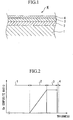
- Fig. 1 is a drawing showing the cross-sectional structure of a semiconductor wafer (semiconductor substrate) W provided with a strained Si layer of the present invention.
- a first SiGe layer 2 in the form of an incremental composition layer (incremental composition region) in which Ge composite ratio x gradually increases at an increment from 0 to 0.3 in the direction of deposition (towards the surface), is epitaxially grown by vacuum CVD on an Si substrate 1.
- the aforementioned deposition by vacuum CVD uses H 2 for the carrier gas and SiH 4 and GeH 4 for the source gas.
- a second SiGe layer 3 in the form of a constant composition and buffer, is epitaxially grown at the final Ge composite ratio (0.3) of the first SiGe layer 2 in said first SiGe layer 2.
- These first SiGe layer 2 and second SiGe layer 3 function as an SiGe buffer layer for depositing a strained Si layer.
- heat treatment is performed either during or after formation of these first SiGe layer 2 and second SiGe layer 3 to cause worsening of surface roughness to occur on the SiGe layer in advance.
- the conditions of this heat treatment are set to a temperature that exceeds the temperature of epitaxial growth of the SiGe layers such as 800-1100°C, and to a heat treatment time of 1-200 minutes.
- the supply of source gas is temporarily interrupted during deposition of the second SiGe layer 3, and then annealed after raising the temperature to 1000°C while still in this state. Following this annealing treatment, the temperature is lowered to the deposition temperature of the second SiGe layer 3, supply of the source gas is resumed and the remaining deposition is performed.
- the surface of the second SiGe layer 3 in which irregularities have formed in the surface by worsening of surface roughness caused by heat treatment is polished by chemical mechanical polishing (CMP) and so forth to flatten the surface and remove the irregularities that formed due to worsening of surface roughness.
- CMP chemical mechanical polishing
- the film thicknesses of the aforementioned first SiGe layer 2 and second SiGe layer 3 are set to 1.5 ⁇ m and 0.75 ⁇ m, respectively.
- a strained Si layer 4 is then formed by epitaxially growing an Si layer on the polished second SiGe layer 3 to produce a semiconductor wafer W
- heat treatment is performed at a temperature that exceeds the temperature of the epitaxial growth either during or after the formation of the second SiGe layer 3 by said epitaxial growth, and irregularities in the surface formed during the heat treatment are removed by polishing following the formation of the second SiGe layer 3. Since worsening of surface roughness caused by lattice relaxation and dislocation movement is made to occur in advance by subjecting the substrate to a preliminary heat history, the recurrence of worsening of surface and interface roughness can be prevented during heat treatment in a device production process and so forth.
- first SiGe layer 2 is an incremental composition region in which the Ge composite ratio increases gradually towards the surface, dislocation density particularly on the surface side in the SiGe layer can be inhibited.
- MOSFET field effect transistor
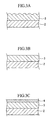
- Fig. 4 shows the schematic structure of a field effect transistor of the present invention.
- an SiO 2 gate oxide film 5 and a gate polysilicon film 6 are sequentially deposited on a strained Si layer 4 on the surface of a semiconductor wafer W provided with the strained Si layer produced in the aforementioned production process.
- a gate electrode (not shown) is then formed by patterning on gate polysilicon film 6 over the section serving as a channel region.
- gate oxide film 5 is also patterned to remove all sections except that beneath the gate electrode. Moreover, an n-type or p-type source region S and drain region D are then formed in a self-aligning manner on the strained Si layer 4 and the second SiGe layer 3 by ion injection using the gate electrode as a mask. Subsequently, a source electrode and drain electrode (not shown) are respectively formed on the source region S and the drain region D to produce an n-type or p-type MOSFET in which the strained Si layer 4 serves as the channel region.
- heat treatment of the SiGe layer was performed during formation of the second SiGe layer in the aforementioned embodiment, heat treatment may also be performed during formation of the first SiGe layer or after formation of the second SiGe layer.
- a semiconductor wafer additionally provided with an SiGe layer on the strained Si layer of the semiconductor substrate W provided with a strained Si layer of the aforementioned embodiment is also included in the present invention.
- the strained Si layer was deposited directly on the second SiGe layer, another SiGe layer may be additionally deposited on the second SiGe layer, and the strained Si layer may be epitaxially grown with said SiGe layer in between.
- a semiconductor wafer having an SiGe layer was produced as a MOSFET substrate in the aforementioned embodiment, it may also be used for a substrate applied to other applications as well.
- the semiconductor substrate of the present invention may also be applied to a substrate for a solar cell.
- a solar cell substrate may be produced by depositing an SiGe layer, in the form of an incremental composition region in which the Ge composite ratio is gradually increased so as to reach 100% Ge on the uppermost surface, on an Si substrate of each of the aforementioned embodiments, and then depositing GaAs (gallium arsenide) thereon. In this case, a high-performance solar cell substrate is obtained having a low dislocation density.
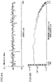
- Graphs of surface roughness and the power spectrum of that roughness are shown in Figs. 5A and 5B, respectively, for the case of performing heat treatment consisting of an annealing temperature of 1000°C and annealing time of 10 minutes during deposition of the second SiGe layer 3 based on the aforementioned embodiments, and depositing the remaining second SiGe layer 3 after the heat treatment. Furthermore, surface roughness was measured using a Nomarski surface roughness measuring device. In addition, graphs of surface roughness and the power spectrum of that roughness in the case of not performing heat treatment are similarly shown in Figs. 6A and 6B as a comparative example. In the aforementioned graphs of the power spectra of surface roughness, the wavelength of the roughness period is plotted on the horizontal axis, while the intensity for each wavelength component of roughness is plotted on the vertical axis.
- Figs. 5A and 6A in the example of the present invention, surface roughness increased from a root mean square (RMS) value of 3.00 nm to 6.40 nm as compared with the comparative example.
- RMS root mean square
- Figs. 5B and 6B the power spectrum components of several hundred ⁇ m or more increased, indicating that irregularities are occurring on the surface at a period having a large wavelength. Namely, this means that the SiGe layer was subjected to sufficient heat history due to the aforementioned annealing treatment.
- the occurrence of worsening of surface and interface roughness during heat treatment in a device production process can be prevented by removing irregularities in the surface of the second SiGe layer in the aforementioned polishing step.
- surface roughness exhibited an RMS value of 0.60 nm when irregularities in the second SiGe layer surface were removed in the aforementioned polishing step.
- this sample following polishing was subjected to heat treatment consisting of an annealing temperature of 1000°C and annealing time of 10 minutes, there was no worsening of surface roughness.
- an example subjected to annealing treatment and a comparative example not subjected to annealing treatment were prepared, and both were measured with an atomic force microscope (AFM) (to determine roughness in an actual space).
- AFM atomic force microscope
- deposition was carried out with a single-wafer vacuum epitaxial growth system using an Si substrate 1 having a diameter of 200 mm by mixing SiH 4 and GeH 4 into carrier hydrogen and depositing at a pressure of 5000-15000 Pa and temperature of 680-850°C.
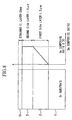
- the production flow chart of these example and comparative example is shown in Fig. 7.
- a first SiGe layer 2, a second SiGe layer 3 and a strained Si layer 10 were deposited at 1.5 ⁇ m, 1.5 ⁇ m and 20 nm, respectively, prior to annealing treatment and polishing treatment. Furthermore, the Ge composite ratio of the second SiGe layer was made to be 0.30.
- pre-polishing annealing treatment was performed for 30 minutes at 1100°C in the presence of flowing nitrogen gas with a horizontal heat treatment oven.
- CMP treatment post-annealing polishing treatment
- ordinary SC1 cleaning was performed following this polishing treatment.
- a second SiGe layer 3 was re-deposited at 0.2 ⁇ m under the same conditions as the initial deposition, and a strained Si layer 4 was deposited at 20 nm.
- heat treatment was additionally performed for 30 minutes at 1100°C in the presence of flowing nitrogen gas using a horizontal heat treatment oven in order to compare the heat resistance of the present example and comparative example in the form of a simulated test of heat treatment during a device production process.
- Measurement by AFM and measurement using a surface roughness gauge were performed for the present example and comparative example produced in the manner described above. Furthermore, measurements were made before polishing and before and after the device heat treatment simulated test, respectively, for the sake of comparison.
- AFM measurement was performed using a scanning region measuring 20 ⁇ m x 20 ⁇ m, while measurement using the surface roughness gauge was performed using a scanning line length of 1 mm, cutoff length of 0.1 mm and in measurement steps of 0.2 ⁇ m.
- the present example exhibited an extremely small change in RMS following the heat treatment simulated test as compared with the comparative example, thereby demonstrating a satisfactory surface state.
- Fig. 9 the power spectra resulting from Fourier transformation of the results of AFM measurement are shown in Fig. 9. It can be understood from these spectra that in the case of the present example, there is considerable improvement in the power spectrum of 5 x 10 -1 cycles/ ⁇ m in terms of spatial frequency and 2 ⁇ m or less in terms of wavelength as compared with the comparative example. Namely, a considerable improvement in worsening of micro-roughness due to heat history is indicated for the present example as compared with the comparative example.
- micro-roughness is known to have a strong effect on deterioration of hole mobility, thereby demonstrating that the present invention can result in a considerable improvement in the production of p-type transistors (which are essential for the production of CMOS) using strained Si wafers.
- the semiconductor substrate and semiconductor substrate production method of the present invention since heat treatment is performed at a temperature that exceeds the temperature of epitaxial growth either during or after formation of an SiGe layer by said epitaxial growth, and surface irregularities formed due to heat treatment are removed by polishing after forming the SiGe layer, even if heat treatment is performed in a device production process and so forth on this substrate from which surface irregularities resulting from preliminary heat history have been removed by polishing, recurrence of worsening of surface or interface roughness can be prevented.
- a substrate can be obtained that is suitable as a substrate for an integrated circuit that uses, for example, a MOSFET having a strained Si layer for a channel region.
- the transistors since the transistors have a channel region in the strained Si layer of the aforementioned semiconductor substrate of the present invention or semiconductor substrate produced according to the aforementioned semiconductor substrate production method of the present invention, even if the transistors are subjected to heat treatment during device production, a high-quality strained Si layer is provided on an SiGe layer having a favorable surface state, and a high-performance MOSFET can be obtained at high yield.
- the present invention is industrially useful.
Landscapes
- Insulated Gate Type Field-Effect Transistor (AREA)
- Recrystallisation Techniques (AREA)
Abstract
Description
P-V value: 43.97 nm
P-V value: 6.69 nm
P-V value: 19.02 nm
P-V value: 10.36 nm
P-V value: 19.57 nm
Claims (7)
- A semiconductor substrate production method in which an SiGe layer is formed on an Si substrate, comprising:a heat treatment step in which heat treatment is performed either during or after the formation of the SiGe layer by epitaxial growth at a temperature that exceeds the temperature of the epitaxial growth, anda polishing step in which irregularities in the surface formed during the heat treatment are removed by polishing following formation of the SiGe layer.
- A semiconductor substrate production method according to claim 1 wherein,
an incremental composition region in which the Ge composite ratio gradually increases towards the surface is formed in at least a portion of the SiGe layer. - A semiconductor substrate production method according to claim 1 or claim 2 wherein,
a strained Si layer is epitaxially grown on the SiGe layer either directly or with another SiGe layer in between after the polishing step. - A field effect transistor production method in which a channel region is formed in a strained Si layer epitaxially grown on an SiGe layer, comprising:forming the channel region in the strained Si layer of a semiconductor substrate produced according to a semiconductor substrate production method according to claim 3.
- A semiconductor substrate in which an SiGe layer is formed on an Si substrate produced according to a semiconductor substrate production method according to claim 1 or claim 2.
- A semiconductor substrate in which a strained Si layer is formed on an Si substrate with an SiGe layer in between produced according to a semiconductor substrate production method according to claim 3.
- A field effect transistor in which a channel region is formed in a strained Si layer epitaxially grown on an SiGe layer that is produced according to a field effect transistor production method according to claim 4.
Applications Claiming Priority (3)
| Application Number | Priority Date | Filing Date | Title |
|---|---|---|---|
| JP2001253175 | 2001-08-23 | ||
| JP2001253175 | 2001-08-23 | ||
| PCT/JP2002/008509 WO2003019632A1 (en) | 2001-08-23 | 2002-08-23 | Production method for semiconductor substrate and production method for field effect transistor and semiconductor substrate and field effect transistor |
Publications (3)
| Publication Number | Publication Date |
|---|---|
| EP1437765A1 true EP1437765A1 (en) | 2004-07-14 |
| EP1437765A4 EP1437765A4 (en) | 2010-03-17 |
| EP1437765B1 EP1437765B1 (en) | 2018-12-26 |
Family
ID=19081546
Family Applications (1)
| Application Number | Title | Priority Date | Filing Date |
|---|---|---|---|
| EP02767854.9A Expired - Lifetime EP1437765B1 (en) | 2001-08-23 | 2002-08-23 | Production method for semiconductor substrate and production method for field effect transistor |
Country Status (6)
| Country | Link |
|---|---|
| US (1) | US7056789B2 (en) |
| EP (1) | EP1437765B1 (en) |
| JP (1) | JP2003158075A (en) |
| KR (1) | KR100571333B1 (en) |
| TW (1) | TWI260698B (en) |
| WO (1) | WO2003019632A1 (en) |
Cited By (2)
| Publication number | Priority date | Publication date | Assignee | Title |
|---|---|---|---|---|
| WO2006032298A1 (en) * | 2004-09-22 | 2006-03-30 | S.O.I.Tec Silicon On Insulator Technologies | Planarization of epitaxial heterostructures including thermal treatment |
| GB2420222A (en) * | 2004-11-13 | 2006-05-17 | Iqe Silicon Compounds Ltd | Enhanced carrier mobility in strained semiconductor layers through smoothing surface treatment |
Families Citing this family (15)
| Publication number | Priority date | Publication date | Assignee | Title |
|---|---|---|---|---|
| JP4207548B2 (en) | 2002-11-28 | 2009-01-14 | 株式会社Sumco | Semiconductor substrate manufacturing method, field effect transistor manufacturing method, semiconductor substrate, and field effect transistor |
| US6946373B2 (en) * | 2002-11-20 | 2005-09-20 | International Business Machines Corporation | Relaxed, low-defect SGOI for strained Si CMOS applications |
| US7118995B2 (en) | 2004-05-19 | 2006-10-10 | International Business Machines Corporation | Yield improvement in silicon-germanium epitaxial growth |
| US7202145B2 (en) * | 2004-06-03 | 2007-04-10 | Taiwan Semiconductor Manufacturing Company | Strained Si formed by anneal |
| EP1605498A1 (en) * | 2004-06-11 | 2005-12-14 | S.O.I. Tec Silicon on Insulator Technologies S.A. | A method of manufacturing a semiconductor wafer |
| US7172930B2 (en) * | 2004-07-02 | 2007-02-06 | International Business Machines Corporation | Strained silicon-on-insulator by anodization of a buried p+ silicon germanium layer |
| US7384829B2 (en) | 2004-07-23 | 2008-06-10 | International Business Machines Corporation | Patterned strained semiconductor substrate and device |
| KR100592749B1 (en) | 2004-11-17 | 2006-06-26 | 한국전자통신연구원 | High-voltage field effect transistor having a heterogeneous structure of silicon and silicon germanium and a method of manufacturing the same |
| JP2006210698A (en) * | 2005-01-28 | 2006-08-10 | Toshiba Ceramics Co Ltd | Strained silicon wafer |
| US7528040B2 (en) | 2005-05-24 | 2009-05-05 | Cree, Inc. | Methods of fabricating silicon carbide devices having smooth channels |
| EP2104135B1 (en) * | 2008-03-20 | 2013-06-12 | Siltronic AG | A semiconductor wafer with a heteroepitaxial layer and a method for producing the wafer |
| JP2010016078A (en) * | 2008-07-02 | 2010-01-21 | Shin Etsu Handotai Co Ltd | Silicon monocrystal wafer, method for manufacturing the silicon monocrystal wafer and method for evaluating the silicon monocrystal wafer |
| KR101538742B1 (en) * | 2009-02-25 | 2015-07-30 | 삼성전자주식회사 | Synthesis method for nanowires |
| TWI702534B (en) * | 2019-07-10 | 2020-08-21 | 尼克森微電子股份有限公司 | Simulation method of power metal oxide semiconductor transistor |
| US20240038531A1 (en) * | 2022-07-27 | 2024-02-01 | Applied Materials, Inc. | Substrate modification for superlattice critical thickness improvement |
Family Cites Families (16)
| Publication number | Priority date | Publication date | Assignee | Title |
|---|---|---|---|---|
| JPS5818928A (en) * | 1981-07-28 | 1983-02-03 | Nec Corp | Manufacture of semiconductor device |
| US5221413A (en) | 1991-04-24 | 1993-06-22 | At&T Bell Laboratories | Method for making low defect density semiconductor heterostructure and devices made thereby |
| US5442205A (en) * | 1991-04-24 | 1995-08-15 | At&T Corp. | Semiconductor heterostructure devices with strained semiconductor layers |
| CA2062134C (en) * | 1991-05-31 | 1997-03-25 | Ibm | Heteroepitaxial layers with low defect density and arbitrary network parameter |
| DE4438380C1 (en) * | 1994-10-27 | 1996-01-25 | Inst Halbleiterphysik Gmbh | Depositing single crystalline mixed crystal layer of germanium silicide |
| US6039803A (en) | 1996-06-28 | 2000-03-21 | Massachusetts Institute Of Technology | Utilization of miscut substrates to improve relaxed graded silicon-germanium and germanium layers on silicon |
| DE69827824T3 (en) * | 1997-06-24 | 2009-09-03 | Massachusetts Institute Of Technology, Cambridge | CONTROL OF SEVENING DENSITY THROUGH THE USE OF GRADIENT LAYERS AND BY PLANARIZATION |
| JP3727449B2 (en) * | 1997-09-30 | 2005-12-14 | シャープ株式会社 | Method for producing semiconductor nanocrystal |
| FR2773177B1 (en) | 1997-12-29 | 2000-03-17 | France Telecom | PROCESS FOR OBTAINING A SINGLE-CRYSTAL GERMANIUM OR SILICON LAYER ON A SILICON OR SINGLE-CRYSTAL GERMANIUM SUBSTRATE, RESPECTIVELY, AND MULTILAYER PRODUCTS OBTAINED |
| JP4258034B2 (en) | 1998-05-27 | 2009-04-30 | ソニー株式会社 | Semiconductor device and manufacturing method of semiconductor device |
| US6506669B1 (en) * | 1998-06-30 | 2003-01-14 | Matsushita Electric Industrial Co., Ltd. | Method of fabricating a thin film transistor |
| CN1168147C (en) | 1999-01-14 | 2004-09-22 | 松下电器产业株式会社 | Manufacturing method of semiconductor crystal |
| US6503773B2 (en) | 2000-01-20 | 2003-01-07 | Amberwave Systems Corporation | Low threading dislocation density relaxed mismatched epilayers without high temperature growth |
| US6524935B1 (en) * | 2000-09-29 | 2003-02-25 | International Business Machines Corporation | Preparation of strained Si/SiGe on insulator by hydrogen induced layer transfer technique |
| US6750119B2 (en) * | 2001-04-20 | 2004-06-15 | International Business Machines Corporation | Epitaxial and polycrystalline growth of Si1-x-yGexCy and Si1-yCy alloy layers on Si by UHV-CVD |
| US20020168802A1 (en) * | 2001-05-14 | 2002-11-14 | Hsu Sheng Teng | SiGe/SOI CMOS and method of making the same |
-
2002
- 2002-08-19 JP JP2002238118A patent/JP2003158075A/en active Pending
- 2002-08-22 TW TW091119202A patent/TWI260698B/en not_active IP Right Cessation
- 2002-08-23 KR KR1020047002384A patent/KR100571333B1/en not_active Expired - Fee Related
- 2002-08-23 US US10/487,526 patent/US7056789B2/en not_active Expired - Lifetime
- 2002-08-23 EP EP02767854.9A patent/EP1437765B1/en not_active Expired - Lifetime
- 2002-08-23 WO PCT/JP2002/008509 patent/WO2003019632A1/en not_active Ceased
Cited By (2)
| Publication number | Priority date | Publication date | Assignee | Title |
|---|---|---|---|---|
| WO2006032298A1 (en) * | 2004-09-22 | 2006-03-30 | S.O.I.Tec Silicon On Insulator Technologies | Planarization of epitaxial heterostructures including thermal treatment |
| GB2420222A (en) * | 2004-11-13 | 2006-05-17 | Iqe Silicon Compounds Ltd | Enhanced carrier mobility in strained semiconductor layers through smoothing surface treatment |
Also Published As
| Publication number | Publication date |
|---|---|
| JP2003158075A (en) | 2003-05-30 |
| KR100571333B1 (en) | 2006-04-14 |
| KR20040027901A (en) | 2004-04-01 |
| TWI260698B (en) | 2006-08-21 |
| US20040245552A1 (en) | 2004-12-09 |
| US7056789B2 (en) | 2006-06-06 |
| EP1437765A4 (en) | 2010-03-17 |
| WO2003019632A1 (en) | 2003-03-06 |
| EP1437765B1 (en) | 2018-12-26 |
Similar Documents
| Publication | Publication Date | Title |
|---|---|---|
| KR100778196B1 (en) | Semiconductor substrate, field-effect transistor, and their production methods | |
| US7056789B2 (en) | Production method for semiconductor substrate and production method for field effect transistor and semiconductor substrate and field effect transistor | |
| US8188512B2 (en) | Growth of germanium epitaxial thin film with negative photoconductance characteristics and photodiode using the same | |
| JP5639248B2 (en) | Semiconductor heterostructures with reduced dislocation pileup and related methods | |
| US8187377B2 (en) | Non-contact etch annealing of strained layers | |
| EP1197992B1 (en) | Production method for a semiconductor wafer | |
| US20070128840A1 (en) | Method of forming thin sgoi wafers with high relaxation and low stacking fault defect density | |
| US8043929B2 (en) | Semiconductor substrate and method for production thereof | |
| WO2004102635A9 (en) | Methods for preserving strained semiconductor layers during oxide layer formation | |
| US7198997B2 (en) | Method for producing semiconductor substrate, method for producing field effect transistor, semiconductor substrate, and field effect transistor | |
| TW201630113A (en) | Method of fabricating a high resistivity semiconductor-on-insulator wafer having a charge trapping layer | |
| US20040219767A1 (en) | SiGe rectification process | |
| US7138650B2 (en) | Semiconductor substrate, field-effect transistor, and their manufacturing method of the same | |
| JP4325139B2 (en) | Manufacturing method of semiconductor substrate and manufacturing method of field effect transistor | |
| JP2003109901A (en) | Method of manufacturing semiconductor substrate, method of manufacturing field effect transistor, semiconductor substrate, and field effect transistor |
Legal Events
| Date | Code | Title | Description |
|---|---|---|---|
| PUAI | Public reference made under article 153(3) epc to a published international application that has entered the european phase |
Free format text: ORIGINAL CODE: 0009012 |
|
| 17P | Request for examination filed |
Effective date: 20040223 |
|
| AK | Designated contracting states |
Kind code of ref document: A1 Designated state(s): AT BE BG CH CY CZ DE DK EE ES FI FR GB GR IE IT LI LU MC NL PT SE SK TR |
|
| AX | Request for extension of the european patent |
Extension state: AL LT LV MK RO SI |
|
| RAP1 | Party data changed (applicant data changed or rights of an application transferred) |
Owner name: SUMCO CORPORATION |
|
| A4 | Supplementary search report drawn up and despatched |
Effective date: 20100215 |
|
| 17Q | First examination report despatched |
Effective date: 20100525 |
|
| GRAP | Despatch of communication of intention to grant a patent |
Free format text: ORIGINAL CODE: EPIDOSNIGR1 |
|
| INTG | Intention to grant announced |
Effective date: 20180817 |
|
| RBV | Designated contracting states (corrected) |
Designated state(s): DE FR GB |
|
| RIN1 | Information on inventor provided before grant (corrected) |
Inventor name: MIZUSHIMA,KAZUKI Inventor name: SHIONO, ICHIRO Inventor name: YAMAGUCHI, KENJI |
|
| GRAS | Grant fee paid |
Free format text: ORIGINAL CODE: EPIDOSNIGR3 |
|
| GRAA | (expected) grant |
Free format text: ORIGINAL CODE: 0009210 |
|
| RIN1 | Information on inventor provided before grant (corrected) |
Inventor name: YAMAGUCHI, KENJI Inventor name: MIZUSHIMA,KAZUKI Inventor name: SHIONO, ICHIRO |
|
| AK | Designated contracting states |
Kind code of ref document: B1 Designated state(s): DE FR GB |
|
| REG | Reference to a national code |
Ref country code: GB Ref legal event code: FG4D |
|
| REG | Reference to a national code |
Ref country code: DE Ref legal event code: R096 Ref document number: 60249743 Country of ref document: DE |
|
| RIC2 | Information provided on ipc code assigned after grant |
Ipc: H01L 21/205 20060101AFI20030310BHEP Ipc: H01L 21/336 20060101ALI20030310BHEP |
|
| REG | Reference to a national code |
Ref country code: DE Ref legal event code: R097 Ref document number: 60249743 Country of ref document: DE |
|
| PLBE | No opposition filed within time limit |
Free format text: ORIGINAL CODE: 0009261 |
|
| STAA | Information on the status of an ep patent application or granted ep patent |
Free format text: STATUS: NO OPPOSITION FILED WITHIN TIME LIMIT |
|
| 26N | No opposition filed |
Effective date: 20190927 |
|
| PGFP | Annual fee paid to national office [announced via postgrant information from national office to epo] |
Ref country code: FR Payment date: 20200821 Year of fee payment: 19 Ref country code: GB Payment date: 20200826 Year of fee payment: 19 Ref country code: DE Payment date: 20200819 Year of fee payment: 19 |
|
| REG | Reference to a national code |
Ref country code: DE Ref legal event code: R119 Ref document number: 60249743 Country of ref document: DE |
|
| GBPC | Gb: european patent ceased through non-payment of renewal fee |
Effective date: 20210823 |
|
| PG25 | Lapsed in a contracting state [announced via postgrant information from national office to epo] |
Ref country code: GB Free format text: LAPSE BECAUSE OF NON-PAYMENT OF DUE FEES Effective date: 20210823 Ref country code: FR Free format text: LAPSE BECAUSE OF NON-PAYMENT OF DUE FEES Effective date: 20210831 Ref country code: DE Free format text: LAPSE BECAUSE OF NON-PAYMENT OF DUE FEES Effective date: 20220301 |