EP1437759A2 - Electron beam device - Google Patents
Electron beam device Download PDFInfo
- Publication number
- EP1437759A2 EP1437759A2 EP04000153A EP04000153A EP1437759A2 EP 1437759 A2 EP1437759 A2 EP 1437759A2 EP 04000153 A EP04000153 A EP 04000153A EP 04000153 A EP04000153 A EP 04000153A EP 1437759 A2 EP1437759 A2 EP 1437759A2
- Authority
- EP
- European Patent Office
- Prior art keywords
- detector
- sample
- electron beam
- field
- dark
- Prior art date
- Legal status (The legal status is an assumption and is not a legal conclusion. Google has not performed a legal analysis and makes no representation as to the accuracy of the status listed.)
- Granted
Links
Images




Classifications
-
- H—ELECTRICITY
- H01—ELECTRIC ELEMENTS
- H01J—ELECTRIC DISCHARGE TUBES OR DISCHARGE LAMPS
- H01J37/00—Discharge tubes with provision for introducing objects or material to be exposed to the discharge, e.g. for the purpose of examination or processing thereof
- H01J37/26—Electron or ion microscopes; Electron or ion diffraction tubes
- H01J37/28—Electron or ion microscopes; Electron or ion diffraction tubes with scanning beams
-
- H—ELECTRICITY
- H01—ELECTRIC ELEMENTS
- H01J—ELECTRIC DISCHARGE TUBES OR DISCHARGE LAMPS
- H01J37/00—Discharge tubes with provision for introducing objects or material to be exposed to the discharge, e.g. for the purpose of examination or processing thereof
- H01J37/02—Details
- H01J37/244—Detectors; Associated components or circuits therefor
Definitions
- the present invention relates to an electron beam device and more particularly to a scanning electron microscope or its similar device capable of observing sample images (STEM images) as those of a transmission electron microscope.
- a scanning electron microscope scans an electron beam on a target sample and detects secondary or reflected electrons from the sample to obtain a sample image. If the sample to observe is a thin film of about 100 nm, most of the scanning electron beam transmits the sample. The intensity and scattering angle of the electrons of the beam that transmits the sample depend on the local state, thickness, and atom type of the sample. Such transmission electrons are detected and displayed to obtain the scanning transmission electron microscopy (STEM) image of the sample.
- STEM image is divided into bright-field and dark-field images. Different signals are used to detect bright-field images and dark-field images. Bright-field images are obtained by detecting only the electrons that transmit the sample without scattering in the sample. The dark-field images are obtained by detecting the electrons that scatter in and transmit the sample.
- a circular detector is used for bright-field images while a torus detector is used for dark-field images.
- Fig. 2 shows a block diagram of a general conventional STEM device.
- the general STEM device is similar in configuration to a transmission electron microscope (TEM) having an acceleration voltage of about 200 kV.
- TEM transmission electron microscope
- a primary electron beam 1 emitted from an electron gun 2 is accelerated by an anode 4, focused by a first focusing lens 5, then scanned on a thin film sample 9 by a deflection coil 8.
- Electrons that transmit the thin film sample 9 disposed between upper and lower magnetic poles 12a and 12b of an objective lens 11 are focused by a control lens 22 disposed under the objective lens 11 so that the control lens 22 can control their scattering angles detected by a dark-field detector 14.
- Dark-field signals comprising elastic scattering electrons 13 are thus detected by the dark-field detector 14.
- Electrons 15 that transmit the dark-field detector 14 are detected by a bright-field detector 17 disposed still under the control lens 22.
- the patent document 1 discloses a method for observing a sample using only one detector in which dark-field signals and bright-field signals are switched over by selecting the position of either bright-field image iris or dark-field image iris retained on a common iris base respectively.
- the patent document 2 discloses a method for enabling a scattering angle range to be selected using a plurality of irises disposed in a plurality of stages. The irises are all similar in mechanism to a camera shutter.
- Patent document 1 Official gazette of JP-A No. 169429/1995
- Patent document 2 Official gazette of JP-A No. 139988/1994
- the objective lens of a STEM device is designed for observing thin films.
- a thin film sample 9 is disposed approximately in the center between the upper and lower magnetic poles 12a and 12b of the objective lens 11.
- the STEM device is specially structured to observe bulky samples at high resolution.
- the sample observation plane (place where the primary electron beam is focused) is one-sided to become closer to the upper magnetic pole 12a of the objective lens 11. Consequently, if a STEM observation is to be made for a thin film sample put there, electrons 13 or 15 that transmit the thin film sample come to be affected strongly by the objective lens 11 until they pass the lower magnetic pole 12b of the objective lens 11.
- the electrons are thus focused again before they pass the lower magnetic pole 12b (Fig. 5).
- the electrons transmitting the lower magnetic pole 12b of the objective lens 11 go under the magnetic pole of the objective lens 11 at angles larger than the angles of the electrons scattering in the sample.
- the acceleration voltage of the primary electron beam drops, the angle itself, at which the incident electron beam scatters in the thin film sample, increases. This is why it has been very difficult for conventional techniques to detect electrons scattering at high angles in the target sample, then transmitting the sample if the STEM observation is made using an in-lens type high resolution scanning electron microscope at an acceleration voltage of 50 kV and under. Because, electrons scattering at high angles in the sample, then transmitting the sample come to hit against the inner wall of the magnetic path provided at a halfway before they reach the control lens (C3) 22 disposed under the objective lens 11 or transmission electron detector.
- an object of the present invention to provide an electron beam device to be employed for a high resolution scanning microscope provided with an in-lens type objective lens and capable of detecting electrons (dark-field signals) that scatter at large angles in a sample, then transmit the sample, which has been difficult to be detected, as well as provided with a mechanism capable of selecting a scattering angle range to enable observation of high contrast STEM images at high resolution in accordance with each sample and/or purpose.
- the present invention disposes a dark-field image detector at a position closer to the lower magnetic pole of an objective lens, for example, between the sample and the lower magnetic pole of the objective lens, at a position under and close to the lower magnetic pole of the objective lens, or at a position under a place where electrons that transmit the sample are focused again and transmission electrons of which scattering angle in the sample is 100 mrad and over are detected.
- This disposition of the transmission electron detector thus makes it possible to detect transmission electrons having large scattering angles.
- the present invention disposes the dark-field transmission electron detector under and close to the lower magnetic pole of the objective lens and provides the electron beam device with means for moving this detector along the light axis. This makes it possible for the electron beam device to change the scattering angle range of transmission electrons detected by the dark-field detector, so that an optimized scattering angle range can be set for each sample.
- the present invention provides the electron beam device with a bright-field detector for detecting transmission electrons (bright-field signal electrons) that transmit the dark-field detector so as to be disposed under the dark-field detector and disposes a deflector and a bright-field iris between the dark-field detector and the bright-field detector.
- This makes it possible for bright-field signals to pass the center of a desired bright-field iris to control the transmission electron detection area.
- An amount of bright-field signals that transmit a thin film sample depends on the thickness of the sample. Therefore, the present invention makes it possible to electrically select a large diameter bright-field iris for thick samples and a small diameter bright-field iris for thin samples.
- the present invention provides the electron beam device with means for dividing the detector of dark-field signal electrons into two or more detection elements so as to select or calculate a signal for each element to be detected. This means makes it possible to display high contrast information of only the electrons scattering and transmitting in a specific direction.
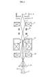
- Fig. 1 shows a block diagram of a scanning electron microscope capable of observing STEM images in an embodiment of the present invention.
- the present invention applies to an in-lens type scanning electron microscope.
- an electron beam 1 emitted from an field-emission electron gun 2 due to the electric field generated by a lead electrode 3 to which a voltage of 3 to 6 kv is applied is accelerated by an anode 4 (to which a voltage of 0.5 to 30 kv is applied), then focused by a first focusing lens 5 (C1 lens) , then unnecessary areas of the beam are removed by an objective lens iris 6. Passing through the objective lens iris 6, the electron beam 1 is focused into a still thinner beam by a second focusing lens 7 (C2 lens) and an objective lens 11. This thinner electron beam 1 is scanned two-dimensionally on a thin film sample 9 having a thickness of about 100 nm put in the objective lens 11 by a two-step deflection coil 8.
- the secondary (or reflected) electron emitted from the sample 9 is detected by a secondary electron detector (or reflection electron detector) 10 installed over the objective lens 11.
- the electron detected by the secondary detector (or reflected electron detector) 10 is then amplified by an amplifier to form a scanning electron microscope image on a CRT 18 synchronized with the deflection coil 8.
- the torus dark-field detector 14 is disposed closely to the objective lens lower magnetic pole 12b so as to detect transmission electrons (elastic scattering electrons) 13 of which scattering angle is 100 mrad and over.
- transmission electrons elastic scattering electrons
- the acceleration voltage is 200 kV
- dark-field images of practical use are obtained if it can detect transmission electrons of which scattering angle is 50 mrad and over. If the acceleration voltage is 50 kV and under, however, it must detect transmission electrons of which scattering angle is at least 100 mrad and over to form dark-field images.
- a bright-field iris 16 is provided between the dark-field detector 14 and the bright-field detector 17, and bright-field signals (non-scattering electrons + non-elastic scattering electrons) 15 that pass the apertures of the bright-field iris 16 are detected as described above, bright-field images are observed.
- the bright-field iris 16 has two or more apertures 20 structured as shown in Fig. 6 and different in size from each other. An amount of bright-field signals to be transmitted depends on the thickness of the thin film sample. Therefore, if the sample is thick, a large diameter bright-field iris is used to improve the S/N ratio.
- the sample is thin, a small diameter bright-field iris is used to obtain high contrast information.
- the bright-field iris 16 shown in Fig. 6 has four apertures different in diameter from each other. However, the number of apertures of the bright-field iris 16 may be changed freely.
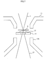
- Fig. 7 shows another example for disposing the dark-field detector in the scanning electron microscope.
- the dark-field detector 14 is disposed between the sample 9 placed in the objective lens 11 and the objective lens lower magnetic pole 12b.
- This disposition of the dark-field detector as shown in Fig. 1 makes it possible for the dark-field detector 14 to detect electrons (elastic scattering electrons 13) having larger scattering angles than those detected when the dark-field detector 14 is disposed under the lower magnetic pole 12b of the objective lens 11 in the scanning electron microscope.
- Fig. 8 shows an illustration for describing how a dark-field detector is disposed between a sample placed in an objective lens and an objective lens lower magnetic pole.
- the dark-field detector 14 is connected to an operation member 25 provided outside a mirror body through a support 23.
- the detector 14 is inserted from outside the mirror body and vacuum-sealed by a vacuum bellows 24. If the sample inclination angle is to increase for observing anything other than STEM images, the detector 14 can be taken out from above the light axis as needed.
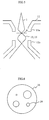
- the dark-field detector 14 may be divided into a plurality of detection elements in the circumferential direction as shown in Fig. 9. If the sample is a crystal, sometimes strong signals are output only in a specific direction due to the diffraction of transmission electrons. If the dark-field detector 14 is divided in such a case, signals having only a specific diffraction angle can be detected. Then, a dark-field signal detected in each divided dark-field detection element is output together with other signals detected by other elements. And, the present invention provides the microscope with means for selecting or calculating the signal from each specific detection element to display high contrast information of only the electrons that scatter and transmit in a specific direction.
- the detector 14 is divided into four detection elements in this embodiment, it may be divided into two or more freely, preferably, as many as possible.
- one of the signals from those divided detection elements is selected by the switches SW1 to SW4, each of which then sets a subtraction/addition operation for each detection element. After that, only the signal selected by the signal addition circuit 30 is added to the object signal.
- Such a configuration of the electron beam device can thus select only the signal output from a desired detection element and/or observe a STEM image with the signals to/from which signals from the detection elements are added/subtracted.
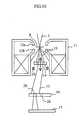
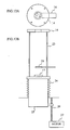
- Fig. 10 shows a cross sectional view of the dark-field detector 14 disposed under the lower magnetic pole 12b of the objective lens 11.
- this disposition of the detector 14 comes to limit the detection angle with respect to each scattering angle up to a certain degree, the problem can be solved by disposing the detector 14 around the cross-over point of transmission electrons shown in Fig. 5; electrons can be detected at scattering angles of at least 100 mrad and over.
- the sample inclination is not limited, thereby loading/unloading of the detector 17 is omitted and the operation becomes easier.
- the deflector 19 for deflecting bright-field signals 15 is disposed between the dark-field detector 14 and the bright-field detector 16.
- the deflector 19 aligns bright-field signals 15 so that they pass through a desired iris hole 20. Consequently, a proper amount of signals can be obtained in accordance with the thickness of each sample during observation of bright-field images. If the sample is thin, bright-field images can be observed at still higher contrast.
- the dark-field detector 14 is structured so that it is moved in the direction along the light axis as shown in Fig. 10. For example, the detector 14 is moved toward the lower magnetic pole 12b of the objective lens to detect transmission electrons having large scattering angles, such as heavy elements (ex., tungsten, Cu, etc.) included in the semiconductor sample and toward a position away from the magnetic pole of the objective lens to observe a sample mainly comprising light elements (ex., a living sample) (to detect transmission electrons having small scattering angles). Consequently, the scattering angle range of transmission electrons detected by the dark-field detector 14 can be changed freely. It is thus possible to obtain high contrast STEM images in a detection range set appropriately for each element included in the target thin film sample.
- transmission electrons having large scattering angles such as heavy elements (ex., tungsten, Cu, etc.) included in the semiconductor sample and toward a position away from the magnetic pole of the objective lens to observe a sample mainly comprising light elements (ex., a living sample) (to detect transmission electrons having small
- Fig. 11 shows an illustration for describing a comparison to be made between dark-field images that come to differ between scattering angle ranges.
- the sample is a thin MO disk.
- the illustration (a) denotes a bright-field image obtained by detecting only the electrons that transmit the sample without scattering in the sample.
- the illustration (b) denotes a dark-field image obtained by detecting transmission electrons having a scattering angle of 100 mrad and over and the illustration (c) denotes a dark-field image obtained by detecting transmission electrons having a scattering angle of 100 mrad and under. Because the detection angle is small and obtained signals are not enough in amount, the contrast is not inverted correctly with respect to the bright-field image in the recording layer. This figure shows that signals of larger scattering angles must be caught to obtain dark-field STEM images of heavy elements.
- Figs. 12A and 12B show a block diagram of the moving means of the dark-field detector 14.
- Fig. 12A shows a top view and Fig. 12B shows a side view.
- the moving means is driven by a motor.
- the dark-field detector 14 is connected to an operation member 25 through a support 23.
- the operation member 25 is also connected to the bright-field detector 17.
- a bright-field iris 16 is fixed from a side of the mirror body between the dark-field detector 14 and the bright-field detector 17.
- the operation member 25 is vacuum-sealed by the vacuum bellows 24 and moved to the dark-field detector 14 along the light axis by a screw 26 driven by a motor 27.
- the present invention therefore, it is possible to detect electrons scattering widely in the target sample and transmitting the sample at a low acceleration voltage, and further to change the detection range of scattering electrons freely to detect only the dark-field signals at a specific diffraction angle, thereby high contrast STEM images are observed appropriately to each sample and purpose.
Landscapes
- Chemical & Material Sciences (AREA)
- Analytical Chemistry (AREA)
- Analysing Materials By The Use Of Radiation (AREA)
Abstract
Description
Claims (9)
- An electron beam device, comprising:wherein said objective lens is an in-lens type one disposed between said sample and an objective lens magnetic pole; andmeans for accelerating an electron beam emitted from an electron source;an objective lens for focusing said accelerated electron beam on a sample;means for scanning said electron beam on said sample two-dimensionally;a transmission electron detector for detecting electrons transmitting said sample; andmeans for recording or displaying said sample with signals output from said transmission electron detector;
wherein said transmission electron detector is disposed under said sample and closely to a lower magnetic pole of said objective lens. - The electron beam device according to claim 1,
wherein said transmission electron detector is disposed between said sample and said lower magnetic pole of said objective lens. - The electron beam device according to claim 1,
wherein said transmission electron detector is disposed under said lower magnetic pole of said objective lens. - The electron beam device according to claim 1,
wherein said transmission electron detector is disposed under a place where electrons transmitting said sample are focused again and electrons scattering at an angle of 100 mrad and over in said sample, then transmitting said sample are detected. - The electron beam device according to claim 1,
wherein said transmission electron detector is structured so as not to detect transmission electrons at its center portion. - An electron beam device, comprising:wherein said transmission electron detector is a dark-field detector that does not detect any transmission electron at its center portion; andmeans for accelerating an electron beam emitted from an electron source;an objective lens for focusing said accelerated electron beam on a sample;means for scanning said electron beam on said sample two-dimensionally;a transmission electron detector for detecting electrons transmitting said sample; andmeans for recording or displaying said sample with signals output from said transmission electron detector;
wherein said electron beam device also includes detector moving means for moving said dark-field detector along a light axis in an area under a lower magnetic pole of said objective lens. - The electron beam device according to claim 6,
wherein said dark-field detector is structured so as to transmit electrons through its center portion; and
wherein said electron beam device also includes a bright-field detector disposed under said dark-field detector, said bright-field detector being used to detect electrons transmitting said center portion of said dark-field detector. - The electron beam device according to claim 7,
wherein said device further includes;
a bright-field iris having two or more apertures and being disposed between said dark-field detector and said bright-field detector; and
alignment means for controlling the positions of electrons transmitting said center portion of said dark-field detector on said bright-field iris so that said electrons pass one of said apertures of said bright-field iris. - The electron beam device according to claim 1,
wherein said dark-field detector is divided into two or more partial detectors in the circumferential direction; and
wherein said electron beam device further includes a calculation device for selecting any of signals detected by said partial detectors or adding/subtracting signals detected by said partial detectors to/from a signal to be output.
Applications Claiming Priority (2)
| Application Number | Priority Date | Filing Date | Title |
|---|---|---|---|
| JP2003000750A JP3776887B2 (en) | 2003-01-07 | 2003-01-07 | Electron beam equipment |
| JP2003000750 | 2003-01-07 |
Publications (3)
| Publication Number | Publication Date |
|---|---|
| EP1437759A2 true EP1437759A2 (en) | 2004-07-14 |
| EP1437759A3 EP1437759A3 (en) | 2008-02-27 |
| EP1437759B1 EP1437759B1 (en) | 2014-07-16 |
Family
ID=32501177
Family Applications (1)
| Application Number | Title | Priority Date | Filing Date |
|---|---|---|---|
| EP04000153.9A Expired - Lifetime EP1437759B1 (en) | 2003-01-07 | 2004-01-07 | Electron beam device with dark field detector |
Country Status (3)
| Country | Link |
|---|---|
| US (3) | US7105816B2 (en) |
| EP (1) | EP1437759B1 (en) |
| JP (1) | JP3776887B2 (en) |
Cited By (6)
| Publication number | Priority date | Publication date | Assignee | Title |
|---|---|---|---|---|
| WO2005006384A3 (en) * | 2003-07-09 | 2005-02-10 | Zeiss Carl Nts Gmbh | Detector system for a scanning electron microscope and scanning electron microscope with a corresponding detector system |
| FR2908235A1 (en) * | 2006-11-07 | 2008-05-09 | Inst Nat Sciences Appliq | Sample e.g. live bio-sample, tomography equipment, has detection unit to detect signal representative of interaction between sample and electron beam, and storing unit to store association between value of signal and beam position |
| CN104897700A (en) * | 2015-06-10 | 2015-09-09 | 北京工业大学 | Device and method for transmission-scattering imaging of nanometer liquid sample in scanning electron microscope |
| EP3379556A1 (en) * | 2017-03-20 | 2018-09-26 | TESCAN Brno, s.r.o. | Scanning transmission electron microscope with a condenser objective system and a method of use thereof |
| EP3379558A1 (en) * | 2017-03-20 | 2018-09-26 | TESCAN Brno, s.r.o. | Scanning transmission electron microscope with an objective electromagnetic lens and a method of use thereof |
| EP3531439A1 (en) * | 2018-02-22 | 2019-08-28 | FEI Company | Intelligent pre-scan in scanning transmission charged particle microscopy |
Families Citing this family (35)
| Publication number | Priority date | Publication date | Assignee | Title |
|---|---|---|---|---|
| JP3776887B2 (en) * | 2003-01-07 | 2006-05-17 | 株式会社日立ハイテクノロジーズ | Electron beam equipment |
| JP4200104B2 (en) * | 2003-01-31 | 2008-12-24 | 株式会社日立ハイテクノロジーズ | Charged particle beam equipment |
| EP1463087B1 (en) * | 2003-03-24 | 2010-06-02 | ICT, Integrated Circuit Testing Gesellschaft für Halbleiterprüftechnik Mbh | Charged particle beam device |
| JP2006190567A (en) * | 2005-01-06 | 2006-07-20 | Hitachi High-Technologies Corp | Electron beam equipment |
| US7433034B1 (en) * | 2005-06-17 | 2008-10-07 | Nanometrics Incorporated | Darkfield defect inspection with spectral contents |
| JP4734135B2 (en) * | 2005-10-19 | 2011-07-27 | 株式会社日立ハイテクノロジーズ | Charged particle beam apparatus, computer program used therefor, and sample image observation method |
| JP4686385B2 (en) * | 2006-03-14 | 2011-05-25 | 株式会社日立ハイテクノロジーズ | Scanning electron microscope |
| JP4307470B2 (en) * | 2006-08-08 | 2009-08-05 | 株式会社日立ハイテクノロジーズ | Charged particle beam apparatus, sample processing method, and semiconductor inspection apparatus |
| JP2008204642A (en) * | 2007-02-16 | 2008-09-04 | Hitachi High-Technologies Corp | Scanning transmission charged particle beam equipment |
| US7755043B1 (en) | 2007-03-21 | 2010-07-13 | Kla-Tencor Technologies Corporation | Bright-field/dark-field detector with integrated electron energy spectrometer |
| JP4977509B2 (en) * | 2007-03-26 | 2012-07-18 | 株式会社日立ハイテクノロジーズ | Scanning electron microscope |
| DE102007026847A1 (en) * | 2007-06-06 | 2008-12-11 | Carl Zeiss Nts Gmbh | Particle beam apparatus and method of use in a particle beam apparatus |
| US8642959B2 (en) | 2007-10-29 | 2014-02-04 | Micron Technology, Inc. | Method and system of performing three-dimensional imaging using an electron microscope |
| JP4597207B2 (en) | 2008-03-31 | 2010-12-15 | 株式会社日立ハイテクノロジーズ | Scanning electron microscope |
| JP5285944B2 (en) * | 2008-04-03 | 2013-09-11 | 株式会社日立ハイテクノロジーズ | Charged particle beam apparatus and sample observation method using charged particle beam |
| US8981294B2 (en) * | 2008-07-03 | 2015-03-17 | B-Nano Ltd. | Scanning electron microscope, an interface and a method for observing an object within a non-vacuum environment |
| JP5649583B2 (en) * | 2008-10-31 | 2015-01-07 | エフ イー アイ カンパニFei Company | Processing end point detection method and apparatus |
| DE102009016861A1 (en) * | 2009-04-08 | 2010-10-21 | Carl Zeiss Nts Gmbh | particle beam |
| EP2446459B1 (en) | 2009-06-24 | 2015-04-01 | Carl Zeiss Microscopy, LLC | Charged particle detectors |
| JP5216739B2 (en) | 2009-10-15 | 2013-06-19 | 株式会社日立ハイテクノロジーズ | Charged particle beam apparatus and film thickness measuring method |
| EP2388796A1 (en) | 2010-05-21 | 2011-11-23 | FEI Company | Simultaneous electron detection |
| US8624186B2 (en) * | 2010-05-25 | 2014-01-07 | Hermes Microvision, Inc. | Movable detector for charged particle beam inspection or review |
| JP6016938B2 (en) * | 2012-10-30 | 2016-10-26 | 株式会社日立ハイテクノロジーズ | Charged particle beam apparatus and observation method using the same |
| EP2959287A4 (en) | 2013-02-20 | 2016-10-19 | Nano Ltd B | ELECTRONIQUE SCANNING MICROSCOPE |
| JP6240754B2 (en) * | 2014-05-09 | 2017-11-29 | 株式会社日立ハイテクノロジーズ | Sample processing method and charged particle beam apparatus |
| JP6533665B2 (en) * | 2015-02-03 | 2019-06-19 | 日本電子株式会社 | Electron microscope and aberration measurement method |
| WO2016151786A1 (en) * | 2015-03-25 | 2016-09-29 | 株式会社 日立ハイテクノロジーズ | Electron microscope |
| US9613779B2 (en) | 2015-11-12 | 2017-04-04 | Ningbo Focus-ebeam Instruments Inc. | Scanning transmission electron microscope with variable axis objective lens and detective system |
| EP3385977B1 (en) * | 2015-12-03 | 2021-07-28 | Matsusada Precision, Inc. | Charged particle beam device and scanning electron microscope |
| DE112016006965B4 (en) * | 2016-07-28 | 2022-05-25 | Hitachi High-Tech Corporation | charged particle beam device |
| CN106769162B (en) * | 2017-02-20 | 2023-06-06 | 广西大学 | Transmission electron microscope magnetic sample preprocessor |
| JP2020017415A (en) * | 2018-07-26 | 2020-01-30 | 株式会社日立ハイテクノロジーズ | Charged particle beam equipment |
| JP6843913B2 (en) * | 2019-03-28 | 2021-03-17 | 日本電子株式会社 | Control method of transmission electron microscope and transmission electron microscope |
| CN115410888B (en) * | 2022-09-16 | 2025-08-19 | 纳克微束(北京)有限公司 | Electron microscope and application method thereof |
| US12676280B2 (en) | 2023-06-12 | 2026-07-07 | Airsem Technologies Ltd. | Charged particle beam devices and membrane assemblies useful therein |
Family Cites Families (11)
| Publication number | Priority date | Publication date | Assignee | Title |
|---|---|---|---|---|
| US3626184A (en) * | 1970-03-05 | 1971-12-07 | Atomic Energy Commission | Detector system for a scanning electron microscope |
| PT75804B (en) | 1981-11-23 | 1985-01-28 | Kaiser Aluminium Chem Corp | Molten metal level control in continuous casting |
| US5866905A (en) * | 1991-05-15 | 1999-02-02 | Hitachi, Ltd. | Electron microscope |
| US6051834A (en) * | 1991-05-15 | 2000-04-18 | Hitachi, Ltd. | Electron microscope |
| JPH09167591A (en) | 1995-12-15 | 1997-06-24 | Hitachi Ltd | Scanning transmission electron microscope |
| JP3730263B2 (en) * | 1992-05-27 | 2005-12-21 | ケーエルエー・インストルメンツ・コーポレーション | Apparatus and method for automatic substrate inspection using charged particle beam |
| JPH06139988A (en) * | 1992-10-23 | 1994-05-20 | Hitachi Ltd | Electron microscope |
| JPH07169429A (en) | 1993-11-05 | 1995-07-04 | Hitachi Ltd | Scanning transmission electron microscope |
| JP3400541B2 (en) | 1994-06-14 | 2003-04-28 | 株式会社日立製作所 | Magnetic microscopic method using scanning electron beam and scanning transmission electron microscope |
| US5981947A (en) * | 1997-02-03 | 1999-11-09 | Nikon Corporation | Apparatus for detecting or collecting secondary electrons, charged-particle beam exposure apparatus comprising same, and related methods |
| JP3776887B2 (en) * | 2003-01-07 | 2006-05-17 | 株式会社日立ハイテクノロジーズ | Electron beam equipment |
-
2003
- 2003-01-07 JP JP2003000750A patent/JP3776887B2/en not_active Expired - Lifetime
-
2004
- 2004-01-07 US US10/751,987 patent/US7105816B2/en not_active Expired - Lifetime
- 2004-01-07 EP EP04000153.9A patent/EP1437759B1/en not_active Expired - Lifetime
-
2006
- 2006-08-07 US US11/499,640 patent/US7355177B2/en not_active Expired - Lifetime
-
2008
- 2008-02-15 US US12/071,152 patent/US7745787B2/en not_active Expired - Lifetime
Non-Patent Citations (1)
| Title |
|---|
| None |
Cited By (11)
| Publication number | Priority date | Publication date | Assignee | Title |
|---|---|---|---|---|
| WO2005006384A3 (en) * | 2003-07-09 | 2005-02-10 | Zeiss Carl Nts Gmbh | Detector system for a scanning electron microscope and scanning electron microscope with a corresponding detector system |
| US7285780B2 (en) | 2003-07-09 | 2007-10-23 | Carl Zeiss Nts Gmbh | Detector system for a scanning electron microscope and a scanning electron microscope incorporating said detector system |
| FR2908235A1 (en) * | 2006-11-07 | 2008-05-09 | Inst Nat Sciences Appliq | Sample e.g. live bio-sample, tomography equipment, has detection unit to detect signal representative of interaction between sample and electron beam, and storing unit to store association between value of signal and beam position |
| CN104897700A (en) * | 2015-06-10 | 2015-09-09 | 北京工业大学 | Device and method for transmission-scattering imaging of nanometer liquid sample in scanning electron microscope |
| CN104897700B (en) * | 2015-06-10 | 2017-09-22 | 北京工业大学 | To the transmission scattering imaging device and method of liquid nano sample in ESEM |
| EP3379556A1 (en) * | 2017-03-20 | 2018-09-26 | TESCAN Brno, s.r.o. | Scanning transmission electron microscope with a condenser objective system and a method of use thereof |
| EP3379558A1 (en) * | 2017-03-20 | 2018-09-26 | TESCAN Brno, s.r.o. | Scanning transmission electron microscope with an objective electromagnetic lens and a method of use thereof |
| EP3531439A1 (en) * | 2018-02-22 | 2019-08-28 | FEI Company | Intelligent pre-scan in scanning transmission charged particle microscopy |
| CN110186943A (en) * | 2018-02-22 | 2019-08-30 | Fei 公司 | Smart pre-scan in scanning transmission charged particle microscope |
| US10665419B2 (en) | 2018-02-22 | 2020-05-26 | Fei Company | Intelligent pre-scan in scanning transmission charged particle microscopy |
| CN110186943B (en) * | 2018-02-22 | 2024-07-02 | Fei公司 | Intelligent pre-scanning in scanning transmission charged particle microscopes |
Also Published As
| Publication number | Publication date |
|---|---|
| US7745787B2 (en) | 2010-06-29 |
| US20080290275A1 (en) | 2008-11-27 |
| US7105816B2 (en) | 2006-09-12 |
| EP1437759A3 (en) | 2008-02-27 |
| EP1437759B1 (en) | 2014-07-16 |
| US7355177B2 (en) | 2008-04-08 |
| US20040183017A1 (en) | 2004-09-23 |
| JP3776887B2 (en) | 2006-05-17 |
| US20060284093A1 (en) | 2006-12-21 |
| JP2004214065A (en) | 2004-07-29 |
Similar Documents
| Publication | Publication Date | Title |
|---|---|---|
| EP1437759B1 (en) | Electron beam device with dark field detector | |
| US6600156B2 (en) | Scanning electron microscope | |
| CN102971824A (en) | Improved contrast for scanning confocal electron microscope | |
| US9613779B2 (en) | Scanning transmission electron microscope with variable axis objective lens and detective system | |
| JPH0233843A (en) | Scanning electronic microscope | |
| EP1063677B1 (en) | Charged particle beam device | |
| JP4354197B2 (en) | Scanning electron microscope | |
| EP3379557A1 (en) | Scanning transmission electron microscope and method for high throughput acquisition of electron scattering angle distribution images | |
| JPS5938701B2 (en) | Scanning electron microscope with two-stage sample stage | |
| US7550724B2 (en) | Electron beam device and its control method | |
| US6376839B1 (en) | SEM for transmission operation with a location-sensitive detector | |
| JP4129088B2 (en) | Scanning transmission electron microscope | |
| JP2001006591A (en) | Charged particle beam equipment | |
| JPH07169429A (en) | Scanning transmission electron microscope | |
| US4121100A (en) | Electron microscope | |
| JP2006156134A (en) | Reflection imaging electron microscope | |
| JPH0234144B2 (en) | ||
| JP3705760B2 (en) | High-performance X-ray image observation system with optimal electron optical design | |
| JP2674993B2 (en) | electronic microscope | |
| WO2026006804A1 (en) | Scanning transmission electron microscope resolution and contrast improvement | |
| JP4111778B2 (en) | Observation method of a sample partially processed into a thin film by a focused ion beam device using an electron microscope | |
| JPH05258700A (en) | Scanning image observing method and scanning electron microscope | |
| TW202333184A (en) | Combining focused ion beam milling and scanning electron microscope imaging | |
| JPH0547331A (en) | Scanning electron microscope | |
| JP2006302523A (en) | Transmission electron microscope with scanning image observation function |
Legal Events
| Date | Code | Title | Description |
|---|---|---|---|
| PUAI | Public reference made under article 153(3) epc to a published international application that has entered the european phase |
Free format text: ORIGINAL CODE: 0009012 |
|
| AK | Designated contracting states |
Kind code of ref document: A2 Designated state(s): AT BE BG CH CY CZ DE DK EE ES FI FR GB GR HU IE IT LI LU MC NL PT RO SE SI SK TR |
|
| AX | Request for extension of the european patent |
Extension state: AL LT LV MK |
|
| 17P | Request for examination filed |
Effective date: 20060331 |
|
| PUAL | Search report despatched |
Free format text: ORIGINAL CODE: 0009013 |
|
| AK | Designated contracting states |
Kind code of ref document: A3 Designated state(s): AT BE BG CH CY CZ DE DK EE ES FI FR GB GR HU IE IT LI LU MC NL PT RO SE SI SK TR |
|
| AX | Request for extension of the european patent |
Extension state: AL LT LV MK |
|
| AKX | Designation fees paid |
Designated state(s): DE NL |
|
| 17Q | First examination report despatched |
Effective date: 20130218 |
|
| RIN1 | Information on inventor provided before grant (corrected) |
Inventor name: AKATSU, MASAHIRO Inventor name: SATO, MITSUGU Inventor name: KAMIYA, CHISATO |
|
| GRAP | Despatch of communication of intention to grant a patent |
Free format text: ORIGINAL CODE: EPIDOSNIGR1 |
|
| RAP1 | Party data changed (applicant data changed or rights of an application transferred) |
Owner name: HITACHI HIGH-TECHNOLOGIES CORPORATION |
|
| INTG | Intention to grant announced |
Effective date: 20140129 |
|
| GRAS | Grant fee paid |
Free format text: ORIGINAL CODE: EPIDOSNIGR3 |
|
| GRAA | (expected) grant |
Free format text: ORIGINAL CODE: 0009210 |
|
| AK | Designated contracting states |
Kind code of ref document: B1 Designated state(s): DE NL |
|
| REG | Reference to a national code |
Ref country code: DE Ref legal event code: R096 Ref document number: 602004045452 Country of ref document: DE Effective date: 20140821 |
|
| REG | Reference to a national code |
Ref country code: NL Ref legal event code: T3 |
|
| REG | Reference to a national code |
Ref country code: DE Ref legal event code: R097 Ref document number: 602004045452 Country of ref document: DE |
|
| PLBE | No opposition filed within time limit |
Free format text: ORIGINAL CODE: 0009261 |
|
| STAA | Information on the status of an ep patent application or granted ep patent |
Free format text: STATUS: NO OPPOSITION FILED WITHIN TIME LIMIT |
|
| 26N | No opposition filed |
Effective date: 20150417 |
|
| PGFP | Annual fee paid to national office [announced via postgrant information from national office to epo] |
Ref country code: NL Payment date: 20191212 Year of fee payment: 17 |
|
| REG | Reference to a national code |
Ref country code: NL Ref legal event code: HC Owner name: HITACHI HIGH-TECH CORPORATION; JP Free format text: DETAILS ASSIGNMENT: CHANGE OF OWNER(S), CHANGE OF OWNER(S) NAME; FORMER OWNER NAME: HITACHI HIGH-TECHNOLOGIES CORPORATION Effective date: 20200402 |
|
| PGFP | Annual fee paid to national office [announced via postgrant information from national office to epo] |
Ref country code: DE Payment date: 20191224 Year of fee payment: 17 |
|
| REG | Reference to a national code |
Ref country code: DE Ref legal event code: R082 Ref document number: 602004045452 Country of ref document: DE Representative=s name: STREHL SCHUEBEL-HOPF & PARTNER MBB PATENTANWAE, DE Ref country code: DE Ref legal event code: R081 Ref document number: 602004045452 Country of ref document: DE Owner name: HITACHI HIGH-TECH CORPORATION, JP Free format text: FORMER OWNER: HITACHI HIGH-TECHNOLOGIES CORP., TOKYO, JP |
|
| REG | Reference to a national code |
Ref country code: DE Ref legal event code: R119 Ref document number: 602004045452 Country of ref document: DE |
|
| REG | Reference to a national code |
Ref country code: NL Ref legal event code: MM Effective date: 20210201 |
|
| PG25 | Lapsed in a contracting state [announced via postgrant information from national office to epo] |
Ref country code: NL Free format text: LAPSE BECAUSE OF NON-PAYMENT OF DUE FEES Effective date: 20210201 |
|
| PG25 | Lapsed in a contracting state [announced via postgrant information from national office to epo] |
Ref country code: DE Free format text: LAPSE BECAUSE OF NON-PAYMENT OF DUE FEES Effective date: 20210803 |