EP1436648B1 - Circuit optique integre comportant un reseau selectif planaire (awg) et des amplificateurs optiques integres - Google Patents
Circuit optique integre comportant un reseau selectif planaire (awg) et des amplificateurs optiques integres Download PDFInfo
- Publication number
- EP1436648B1 EP1436648B1 EP02795533A EP02795533A EP1436648B1 EP 1436648 B1 EP1436648 B1 EP 1436648B1 EP 02795533 A EP02795533 A EP 02795533A EP 02795533 A EP02795533 A EP 02795533A EP 1436648 B1 EP1436648 B1 EP 1436648B1
- Authority
- EP
- European Patent Office
- Prior art keywords
- optical
- integrated
- integrated optical
- circuit
- amplifiers
- Prior art date
- Legal status (The legal status is an assumption and is not a legal conclusion. Google has not performed a legal analysis and makes no representation as to the accuracy of the status listed.)
- Expired - Lifetime
Links
Images


Classifications
-
- G—PHYSICS
- G02—OPTICS
- G02B—OPTICAL ELEMENTS, SYSTEMS OR APPARATUS
- G02B6/00—Light guides; Structural details of arrangements comprising light guides and other optical elements, e.g. couplings
- G02B6/10—Light guides; Structural details of arrangements comprising light guides and other optical elements, e.g. couplings of the optical waveguide type
- G02B6/12—Light guides; Structural details of arrangements comprising light guides and other optical elements, e.g. couplings of the optical waveguide type of the integrated circuit kind
- G02B6/12007—Light guides; Structural details of arrangements comprising light guides and other optical elements, e.g. couplings of the optical waveguide type of the integrated circuit kind forming wavelength selective elements, e.g. multiplexer, demultiplexer
- G02B6/12009—Light guides; Structural details of arrangements comprising light guides and other optical elements, e.g. couplings of the optical waveguide type of the integrated circuit kind forming wavelength selective elements, e.g. multiplexer, demultiplexer comprising arrayed waveguide grating [AWG] devices, i.e. with a phased array of waveguides
- G02B6/12019—Light guides; Structural details of arrangements comprising light guides and other optical elements, e.g. couplings of the optical waveguide type of the integrated circuit kind forming wavelength selective elements, e.g. multiplexer, demultiplexer comprising arrayed waveguide grating [AWG] devices, i.e. with a phased array of waveguides characterised by the optical interconnection to or from the AWG devices, e.g. integration or coupling with lasers or photodiodes
-
- G—PHYSICS
- G02—OPTICS
- G02B—OPTICAL ELEMENTS, SYSTEMS OR APPARATUS
- G02B6/00—Light guides; Structural details of arrangements comprising light guides and other optical elements, e.g. couplings
- G02B6/10—Light guides; Structural details of arrangements comprising light guides and other optical elements, e.g. couplings of the optical waveguide type
- G02B6/12—Light guides; Structural details of arrangements comprising light guides and other optical elements, e.g. couplings of the optical waveguide type of the integrated circuit kind
- G02B6/12004—Combinations of two or more optical elements
-
- G—PHYSICS
- G02—OPTICS
- G02B—OPTICAL ELEMENTS, SYSTEMS OR APPARATUS
- G02B6/00—Light guides; Structural details of arrangements comprising light guides and other optical elements, e.g. couplings
- G02B6/10—Light guides; Structural details of arrangements comprising light guides and other optical elements, e.g. couplings of the optical waveguide type
- G02B6/12—Light guides; Structural details of arrangements comprising light guides and other optical elements, e.g. couplings of the optical waveguide type of the integrated circuit kind
- G02B6/12007—Light guides; Structural details of arrangements comprising light guides and other optical elements, e.g. couplings of the optical waveguide type of the integrated circuit kind forming wavelength selective elements, e.g. multiplexer, demultiplexer
-
- G—PHYSICS
- G02—OPTICS
- G02B—OPTICAL ELEMENTS, SYSTEMS OR APPARATUS
- G02B6/00—Light guides; Structural details of arrangements comprising light guides and other optical elements, e.g. couplings
- G02B6/10—Light guides; Structural details of arrangements comprising light guides and other optical elements, e.g. couplings of the optical waveguide type
- G02B6/12—Light guides; Structural details of arrangements comprising light guides and other optical elements, e.g. couplings of the optical waveguide type of the integrated circuit kind
- G02B2006/12035—Materials
- G02B2006/12038—Glass (SiO2 based materials)
-
- G—PHYSICS
- G02—OPTICS
- G02B—OPTICAL ELEMENTS, SYSTEMS OR APPARATUS
- G02B6/00—Light guides; Structural details of arrangements comprising light guides and other optical elements, e.g. couplings
- G02B6/10—Light guides; Structural details of arrangements comprising light guides and other optical elements, e.g. couplings of the optical waveguide type
- G02B6/12—Light guides; Structural details of arrangements comprising light guides and other optical elements, e.g. couplings of the optical waveguide type of the integrated circuit kind
- G02B2006/12083—Constructional arrangements
- G02B2006/12111—Fibre
-
- G—PHYSICS
- G02—OPTICS
- G02B—OPTICAL ELEMENTS, SYSTEMS OR APPARATUS
- G02B6/00—Light guides; Structural details of arrangements comprising light guides and other optical elements, e.g. couplings
- G02B6/10—Light guides; Structural details of arrangements comprising light guides and other optical elements, e.g. couplings of the optical waveguide type
- G02B6/12—Light guides; Structural details of arrangements comprising light guides and other optical elements, e.g. couplings of the optical waveguide type of the integrated circuit kind
- G02B2006/12133—Functions
- G02B2006/12164—Multiplexing; Demultiplexing
Definitions
- the present invention is related to optical systems and components, and in particular to optical systems with integrated optical components.
- a typical optical network - includes transceivers, amplifiers, multiplexers and demultiplexers, amplifiers, switches and other components.
- Each transmitting portion of a transceiver converts an electrical signal to an optical signal and launches the optical signal into an optical fiber.
- a multiplexer combines the individual optical signals from each optical fiber into a multiple channel optical signal and launches the multiple channel optical signal into an optical fiber.
- a demultiplexer separates the channels out of the multiple-channel optical signal and launches them into separate fibers. Then each receiving portion of a transceiver accepts an optical signal from a fiber and converts it to an electric signal.
- optical network components are discrete components in that each component performs a single function and is connected by optical fibers to other components.
- AMG arrayed waveguide grating
- demultiplexer is produced on one separate integrated circuit (or chip).
- Erbium doped fiber amplifiers are also large and bulky subsystems composed of discrete components (the spool of erbium-doped optical fiber, laser to produce pump light, circulators to prevent light back-reflection, fiber combiners to combine pump light and signal light, and other components).
- EDWA erbium doped waveguide amplifiers
- discrete amplifiers on chip have been fabricated as described in "8-mW Threshold Er 3+ -Doped Planar Waveguide Amplifier," by Ruby N. Gosh, et al., published in IEEE Photonics Technology Letters, Vol. 8, No. 4, April 1996, as described in “Integrate Planar Waveguide Amplifier with 15dB gain at 1550nm,” by J.
- optical network components described above are usually interconnected using optical fiber and fiber connectors.
- Fiber-to-component interfaces and fiber connectors contribute to optical signal power loss, which causes the need to install even more amplifiers to keep the signal above the noise level.
- the installation, test, reconfiguration of networks is becoming prohibitively difficult and expensive.
- WO 98/32196 discusses an integrated semiconductor multi-wavelength transmitter having an arrayed waveguide grating including multiple grating optical waveguides connected between two star coupling regions.
- the multi-wavelength signal from a first coupling region is reflected from a mirrored surface back into the first coupling region and the arrayed waveguide grating, the mirrored surface thus forming one end of the optical cavity.
- Each single-wavelength output from the second coupling region is split into two parts, the first part passing through a gain region and being reflected back from the mirrored surface while the second part passes through modulators and enters the first coupler.
- the multi-wavelength signal output by the second coupling region thereby contains modulated carriers for all wavelengths.
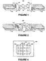
- FIG. 1 is a high-level block diagram of a prior art optical network 100.
- the optical network 100 may implement dense wavelength division multiplexing (DWDM), in which multiple wavelengths of light each carrying a separate data stream are combined on a single optical fiber and then separated again at the receiving end.
- DWDM dense wavelength division multiplexing
- Common wavelengths include 1530 to 1560 nanometers.
- the optical network 100 includes a set of transceivers 102 and 108, which may be n transceivers, and which may launch and receive optical signals into and from optical fibers 112 and 114, respectively, which also may be n optical fibers.
- the optical fibers 112 and 114 may couple n single channel optical signals to and from multiplexers/demultiplexers 104 and 106, respectively.
- the multiplexer/demultiplexer 104 is a discrete component that performs dense wavelength division multiplexing to combine n single channel optical signals received from the transceivers 102 to produce a multiple channel optical signal.
- the multiplexer/demultiplexer 106 also is a discrete component that performs dense wavelength division demultiplexing to separate n single channel optical signals from a multiple channel optical signal, respectively.
- the multiplexers/demultiplexers 104 and 106 may be based on thin film filters or fiber Bragg gratings.
- the multiplexers/demultiplexers 104 and 106 also may be an integrated circuit such as an arrayed waveguide grating (AWG).
- AMG arrayed waveguide grating
- the optical fibers 120, 122, and 124 are discrete components that couple multiple channel optical signals between the multiplexer/demultiplexer 104, the optical amplifiers 130 and 132, and the multiplexer/demultiplexer 106, as depicted in Figure 1.
- Optical amplifiers 130 and 132 are coupled to the multiplexers/demultiplexers 104 and 106, respectively, to amplify multiple channel optical signals.
- the optical amplifiers 130 and 132 are n discrete optical amplifiers located at remote points in the optical network 100 as well as adjacent to the multiplexers/demultiplexers 104 and 106. Although described with respect to signal propagation in one direction, the optical network 100 commonly operates bi-directionally, which is well known.
- Figure 2 is a high-level block diagram of an optical network 200.
- One feature of the optical network 200 is integrated optical circuits, which combine multiplexers, demultiplexers, and optical amplifiers on a single chip, coupled to transceivers.
- the transceivers 102 and 108 are coupled to integrated optical circuits 202 and 204 via the optical fibers 112 and 114, respectively.
- the integrated optical circuit 202 includes a set of optical amplifiers 206 and a multiplexer 208.
- the integrated optical circuit 204 includes a single optical amplifier 210 and a demultiplexer 212.
- the integrated optical circuit 202 is coupled to the integrated optical circuit 204 via an optical fiber 222. Examples embodiments of the integrated optical circuits 202 and 204 are described in more detail with respect to Figure 3.
- an integrated optical circuit 300 includes at least one optical amplifier 302 coupled to an arrayed waveguide grating (AWG) 304 via a waveguide element 306.
- the integrated optical circuits 202 and 204 also include an optical fiber interface 308, which couples pump light onto the integrated optical circuit 202, an optical fiber interface 310, which couples optical signal light onto the integrated optical circuit 202, and an optical fiber interface 312, which couples optical signal light off of the integrated optical circuit 202.
- Devices suitable for implementing the optical fiber interfaces 308, 310, and 312 are well known.
- the AWG 304 is demultiplexing a multiple channel optical signal from a single optical amplifier 302 into several single channel optical signals via a single waveguide element 306. In an alternative embodiment, the AWG 304 is multiplexing several single channel optical signals from several optical amplifiers 302 via several waveguide elements 306 into a multiple channel optical signal.
- the optical amplifier 302 is coupled to the optical fiber interfaces 308 and 310 via pump light waveguide element 314 and optical signal light waveguide element 316, respectively.
- the optical amplifier 302 includes a combiner 318, which may combine pump light with optical signal light.
- the combiner 318 is formed as an evanescent coupler between the waveguide elements 314 and 316.
- the optical amplifier 302 also includes a gain section 320, which in one embodiment is the waveguide element 314 locally doped (e.g., sputtered) with an active substance, such as erbium or other rare earth ions.
- the AWG 304 performs wavelength division multiplexing by passing light through a grating made up of several optical waveguide elements of predetermined different lengths and shapes.
- the AWG 304 includes an input star coupler 322 and an output star coupler 324, which optically couple two ends of an optical waveguide array 332, respectively, with an input set of waveguide elements 326 and an output set of waveguide elements 328, respectively.
- the output set of waveguide elements 328 are coupled to the optical fiber interface 312. Because all components on the integrated optical circuit 202 are coupled via waveguide elements, there is less optical power loss than encountered when coupling discrete optical components via optical fiber.
- One feature of the example integrated optical circuit 202 is that all of the channels within a multiple channel optical signal being amplified by the optical amplifier 302 are amplified in the gain section 320. Gain in this embodiment may be limited by the total power available from a pump source, however. Moreover, different wavelengths (or channels) experience different amounts of gain as determined by the strength of the coupling of the transition in the active substance (e.g., erbium ions) during amplification. The example optical amplifier 302 amplifies the channel with the greatest incoming amplitude more, which is to the detriment of weaker incoming channels. The non-uniform channel amplification may cause lower signal-to-noise ratios (SNR) for the under-amplified channels. Additionally, AWGs, such as the AWG 304, commonly have a non-uniform transmission spectrum (i.e., dependence of the transmission on wavelength).
- SNR signal-to-noise ratios
- the design of the waveguide elements in the AWG 304 is adjusted to compensate for non-uniform channel amplification.
- the shape and width of the waveguides are varied at the junction between the star couplers 322 and 324 and the waveguide array 332. This produces different distributions of intensity of light at the junction between star coupler 324 and output waveguide elements 328, and therefore different distribution of transmission over the waveguide elements 328.
- FIG. 4 is a high-level block diagram of an alternative example integrated optical circuit 400.
- the example integrated optical circuit 400 includes an AWG 402 coupled to a set of optical amplifiers 404 and an AWG 408 via a set of waveguide elements 408 and 410.
- the example can be included in an optical network such as the optical network 200.
- the example AWG 402 demultiplexes a multiple channel optical signal into several single channel optical signals. Each single channel optical signal is amplified separately by one of the optical amplifiers in the set of optical amplifiers 404.
- the AWG 406 then multiplexes then amplifies single channel optical signals.
- the parameters of each optical amplifier in the set of optical amplifiers 404 are chosen to give equal gain to each channel.
- FIG. 5 is a high-level block diagram of an alternative example integrated optical circuit 500 according to embodiments of the present invention.
- the example integrated optical circuit 500 includes set of optical fiber interfaces 502, which couples pump light onto the integrated optical circuit 500, an optical fiber interface 504, which couples optical signal light onto the integrated optical circuit 500, and a set of optical fiber interfaces 506, which couples optical signal light off of the integrated optical circuit 106.
- Devices suitable for implementing the optical fiber interfaces 502, 504, and 506 are well known.
- the example integrated optical circuit 500 includes an AWG 501, which includes an input star coupler 522 and an output star coupler 524, which may optically couple two ends of an optical waveguide array 532, respectively, with an input set of waveguide elements 526 and an output set of waveguide elements 528, respectively.
- the output set of waveguide elements 528 are coupled to a set of optical amplifiers 505.
- the set of optical amplifiers 505 includes a set of combiners 510 comprised of a set of pump light waveguide elements 512 and a set of optical signal waveguide elements 514.
- the set of optical amplifiers 505 also includes a set of gain sections 520. According to the embodiment illustrated in Figure 5, each individual optical amplifier 505 may amplify one of n single channel optical signals. In one embodiment, the lengths of the individual optical amplifiers are tailored to compensate for the non-uniform gain spectrum of the AWG 501.
- An integrated optical circuit according to embodiments of the present invention is a planar lightwave circuits (PLC) on a silicon substrate manufactured using suitable semiconductor processing equipment.
- Figure 6 is a cross-section diagram 600 showing a process for fabricating integrated optical circuits according to an embodiment of the present invention.
- a layer 604 of silica (SiO 2 ) may be deposited on a silicon substrate 602 to form the lower cladding for optical waveguides, using thermal oxidation, for example.
- a layer 606 of silica, germanium, and erbium e.g., SiO 2 +Ge+ Er 3+
- Figure 7 is a cross-section diagram showing a further process for fabricating an integrated optical circuit according to embodiments of the present invention (e.g., the integrated optical circuits 202, 204, 300, 400, and/or 500).
- an integrated optical circuit e.g., the integrated optical circuits 202, 204, 300, 400, and/or 500.
- several waveguide core elements 702 are formed on the integrated optical circuit 106 using chemical processes to remove all but selective portions of the layer 406 of SiO 2 +Ge+ Er 3+ , by reactive ion etching, for example.
- a layer 720 of SiO 2 may be deposited over the optical waveguide elements 702, using flame hydrolysis deposition or chemical vapor deposition, for example.
- optical network having the integrated optical circuit 106, which integrates optical components onto a single chip.
- First is reduced cost because the individual integrated optical circuits (e.g., optical amplifiers with AWGs) may be fabricated in the same processes as electronic components (e.g., by semiconductor processes in the fabrication facilities). This means that adding more components on the chip provides the functionality of several discrete components for a small increment in price compared with one integrated component.
- Second is power savings because by integrating the components on a single chip there are fewer optical losses because there are fewer connections via optical fiber.
- each discrete component is connected via optical fiber and each connection introduces power losses, and power losses are cumulative across connections.
Claims (13)
- Circuit optique intégré (300 ; 500) comprenant :caractérisé en ce que l'ensemble d'amplificateurs optiques (302 ; 505) et le réseau sélectif planaire (304 ; 501) sont à base de silice.un ensemble d'amplificateurs optiques (302 ; 505) formés dans le circuit optique intégré (300 ; 500) ;un réseau sélectif de planaire (304 ; 501) formé dans le circuit optique intégré (300 ; 500) et couplé à l'ensemble d'amplificateurs optiques (302 ; 505) ; etun ensemble d'éléments formant guides d'ondes (306 ; 528) couplés aux sorties de l'ensemble d'amplificateurs optiques (302 ; 505), le réseau sélectif planaire (304 ; 501) ayant un coupleur en étoile (322 ; 524) couplé à l'ensemble d'éléments de guides d'ondes (306 ; 528) ; et
- Circuit optique intégré selon la revendication 1, dans lequel le réseau sélectif planaire (501) est couplé à des entrées de l'ensemble d'amplificateurs optiques (505) par l'intermédiaire d'un ensemble d'éléments de guides d'ondes d'entrée (528).
- Circuit optique intégré selon la revendication 2, dans lequel le réseau sélectif planaire (304) est couplé à des sorties de l'ensemble d'amplificateurs optiques (302) par l'intermédiaire d'un ensemble d'éléments de guides d'ondes de sortie (306).
- Circuit optique intégré selon la revendication 1, dans lequel l'ensemble d'amplificateurs optiques (302 ; 505) comporte un ensemble de parties à gain (320 ; 520) couplées à l'ensemble d'éléments de guides d'ondes (306 ; 528).
- Circuit optique intégré selon la revendication 1, dans lequel chaque amplificateur optique de l'ensemble d'amplificateurs optiques (302 ; 505) a une longueur prédéterminée pour compenser le spectre de gain non uniforme du réseau sélectif planaire (304 ; 501).
- Circuit optique intégré selon la revendication 5, dans lequel chacun de l'ensemble d'amplificateurs optiques (302 ; 505) comprend un combineur (318 ; 510) pouvant être mis en fonctionnement pour combiner la lumière de pompage et la lumière du signal optique.
- Circuit optique intégré selon la revendication 6, comprenant en outre une interface de pompage (308 ; 502) pour coupler la lumière de pompage à l'ensemble d'amplificateurs optiques (302 ; 505).
- Circuit optique intégré selon la revendication 6, comprenant en outre une interface de signal optique (310 ; 506) pour coupler la lumière de signal optique au réseau sélectif planaire (304 ; 501).
- Circuit optique intégré selon la revendication 1, dans lequel le réseau sélectif planaire (304 ; 501) comporte un groupement de guides d'ondes (332 ; 532), dans lequel la forme et la largeur de chaque guide d'ondes du groupement de guides d'ondes est amené à varier pour produire une répartition de lumière variable dans le groupement de guides d'ondes (332 ; 532) du réseau sélectif planaire.
- Système (200), comprenant :un ensemble d'émetteurs/récepteurs (102, 108 sur la figure 2) pour coupler un ensemble de canaux optiques ; etun circuit optique intégré (202, 204) selon l'une quelconque des revendications précédentes, couplé pour recevoir l'ensemble de canaux optiques provenant de l'ensemble d'émetteurs/récepteurs (102, 108).
- Système selon la revendication 10, comprenant en outre un ensemble de fibres optiques (112, 114 sur la figure 2) pour coupler l'ensemble d'émetteurs/récepteurs (102, 108) au circuit optique intégré (202, 204).
- Système selon la revendication 11, dans lequel l'ensemble de signaux optiques comporte un signal optique à canaux multiples et le réseau sélectif planaire (501) est couplé pour démultiplexer le signal optique à canaux multiples en un ensemble de signaux optiques à canal unique.
- Système selon la revendication 11, dans lequel l'ensemble de signaux optiques comporte un ensemble de signaux optiques à canal unique et le réseau sélectif planaire (304) est couplé pour multiplexer l'ensemble de signaux optiques à canal unique en un signal optique à canaux multiples.
Applications Claiming Priority (3)
| Application Number | Priority Date | Filing Date | Title |
|---|---|---|---|
| US982227 | 2001-10-17 | ||
| US09/982,227 US7050663B2 (en) | 2001-10-17 | 2001-10-17 | Integrated optical circuit having an integrated arrayed waveguide grating (AWG) and optical amplifier(s) |
| PCT/US2002/033423 WO2003034111A2 (fr) | 2001-10-17 | 2002-10-17 | Circuit optique integre comportant un reseau selectif planaire (awg) et des amplificateurs optiques integres |
Publications (2)
| Publication Number | Publication Date |
|---|---|
| EP1436648A2 EP1436648A2 (fr) | 2004-07-14 |
| EP1436648B1 true EP1436648B1 (fr) | 2005-12-21 |
Family
ID=25528961
Family Applications (1)
| Application Number | Title | Priority Date | Filing Date |
|---|---|---|---|
| EP02795533A Expired - Lifetime EP1436648B1 (fr) | 2001-10-17 | 2002-10-17 | Circuit optique integre comportant un reseau selectif planaire (awg) et des amplificateurs optiques integres |
Country Status (11)
| Country | Link |
|---|---|
| US (1) | US7050663B2 (fr) |
| EP (1) | EP1436648B1 (fr) |
| JP (1) | JP4276946B2 (fr) |
| KR (1) | KR100705865B1 (fr) |
| AT (1) | ATE313809T1 (fr) |
| AU (1) | AU2002360286A1 (fr) |
| CA (1) | CA2463627A1 (fr) |
| DE (1) | DE60208225T2 (fr) |
| RU (1) | RU2272308C2 (fr) |
| TW (1) | TW595136B (fr) |
| WO (1) | WO2003034111A2 (fr) |
Families Citing this family (33)
| Publication number | Priority date | Publication date | Assignee | Title |
|---|---|---|---|---|
| US7050663B2 (en) | 2001-10-17 | 2006-05-23 | Intel Corporation | Integrated optical circuit having an integrated arrayed waveguide grating (AWG) and optical amplifier(s) |
| US6731425B1 (en) * | 2002-03-07 | 2004-05-04 | Cisco Technology, Inc. | Modular Raman pump double-multiplexer |
| US20050207000A1 (en) * | 2003-02-04 | 2005-09-22 | Fujitsu Limited | Multipoint monitoring method, monitoring point apparatus, and monitoring station apparatus |
| US7181095B1 (en) | 2003-07-29 | 2007-02-20 | Cisco Technology, Inc. | Low loss, noise filtering multiplexer/demultiplexer for reconfigurable OADMs |
| US7297913B2 (en) * | 2004-04-20 | 2007-11-20 | Diehl Bgt Gmbh & Co. Kg | Module for a laser measuring device |
| US7570844B2 (en) * | 2005-01-18 | 2009-08-04 | Doron Handelman | Photonic integrated circuit device and elements thereof |
| US7397986B2 (en) * | 2005-03-04 | 2008-07-08 | Gemfire Corporation | Optical device with reduced temperature dependence |
| KR100868973B1 (ko) * | 2007-04-13 | 2008-11-17 | (주)휴먼라이트 | 평면 광파 회로를 이용한 영상 분배 장치 |
| US8824897B2 (en) * | 2008-06-04 | 2014-09-02 | Accipiter Systems, Inc. | Optical network systems and methods for operating same |
| KR101329453B1 (ko) | 2009-03-20 | 2013-11-15 | 알까뗄 루슨트 | 다기능 도파관 격자를 갖춘 코히어런트 광학 편향기 |
| CN102045125B (zh) * | 2009-10-26 | 2013-12-04 | 华为技术有限公司 | 一种光分路器、光分路器端口识别方法及装置 |
| US8494315B2 (en) * | 2009-12-17 | 2013-07-23 | Alcatel Lucent | Photonic integrated circuit having a waveguide-grating coupler |
| US9103987B2 (en) | 2010-12-29 | 2015-08-11 | Alcatel Lucent | Optical amplifier for multi-core optical fiber |
| US8548291B2 (en) | 2010-12-29 | 2013-10-01 | Alcatel Lucent | Optical amplifier for multi-core optical fiber |
| KR101357996B1 (ko) * | 2011-01-26 | 2014-02-05 | (주)옵토위즈 | 시분할 수동형 광통신망에서 광선로 종단 장치 간에 광 네트워크 시스템 |
| US20120219292A1 (en) * | 2011-02-25 | 2012-08-30 | Accipiter Systems, Inc. | Optical switch for implementing wave division multiplexing networks |
| US8902488B2 (en) | 2012-06-28 | 2014-12-02 | Accipiter Systems, Inc. | System architecture for an optical switch using wavelength, fiber and polarizaton addressing |
| KR101880034B1 (ko) | 2016-12-08 | 2018-07-19 | (주)엑스엠더블유 | 확장성을 갖는 밀리미터파 증폭기 구조 |
| WO2018118807A1 (fr) | 2016-12-19 | 2018-06-28 | Lawrence Livermore National Security, Llc | Transfert sélectif en longueur d'onde d'énergie optique |
| CN110710139A (zh) * | 2017-03-29 | 2020-01-17 | 芬基波尔有限责任公司 | 具有光置换器的无阻塞全网状数据中心网络 |
| CN110710172A (zh) | 2017-03-29 | 2020-01-17 | 芬基波尔有限责任公司 | 在接入节点组内多路复用分组喷射的无阻塞的任意到任意数据中心网络 |
| US10686729B2 (en) | 2017-03-29 | 2020-06-16 | Fungible, Inc. | Non-blocking any-to-any data center network with packet spraying over multiple alternate data paths |
| CN110741356B (zh) | 2017-04-10 | 2024-03-15 | 微软技术许可有限责任公司 | 多处理器系统中的中继一致存储器管理 |
| US10725825B2 (en) | 2017-07-10 | 2020-07-28 | Fungible, Inc. | Data processing unit for stream processing |
| US10659254B2 (en) | 2017-07-10 | 2020-05-19 | Fungible, Inc. | Access node integrated circuit for data centers which includes a networking unit, a plurality of host units, processing clusters, a data network fabric, and a control network fabric |
| WO2019068017A1 (fr) | 2017-09-29 | 2019-04-04 | Fungible, Inc. | Communication de réseau résilient utilisant une pulvérisation sélective de flux de paquets par trajets multiples |
| US11178262B2 (en) | 2017-09-29 | 2021-11-16 | Fungible, Inc. | Fabric control protocol for data center networks with packet spraying over multiple alternate data paths |
| US10841245B2 (en) | 2017-11-21 | 2020-11-17 | Fungible, Inc. | Work unit stack data structures in multiple core processor system for stream data processing |
| US10540288B2 (en) | 2018-02-02 | 2020-01-21 | Fungible, Inc. | Efficient work unit processing in a multicore system |
| US10929175B2 (en) | 2018-11-21 | 2021-02-23 | Fungible, Inc. | Service chaining hardware accelerators within a data stream processing integrated circuit |
| KR102060987B1 (ko) * | 2018-12-12 | 2019-12-31 | 주식회사 온페이스 | 5g 통신용 광파 회로와 이를 이용한 단일 채널의 전이중 광통신 시스템 |
| US10838149B2 (en) * | 2019-03-05 | 2020-11-17 | Lawrence Livermore National Security, Llc | Dual-core fiber amplifier for separation of thermal and nonlinear effects |
| WO2021113793A1 (fr) * | 2019-12-05 | 2021-06-10 | Ipg Photonics Corporation | Système de transmission cohérente par monofibre bidirectionnelle |
Family Cites Families (13)
| Publication number | Priority date | Publication date | Assignee | Title |
|---|---|---|---|---|
| GB9305977D0 (en) * | 1993-03-23 | 1993-05-12 | Northern Telecom Ltd | Transmission system incorporating optical amplifiers |
| US5459801A (en) * | 1993-10-29 | 1995-10-17 | Rutgers University | Coupler used to fabricate add-drop devices, dispersion compensators, amplifiers, oscillators, superluminescent devices, and communications systems |
| JPH09321740A (ja) | 1996-05-31 | 1997-12-12 | Fujitsu Ltd | 波長分割多重のための光増幅器 |
| WO1998032196A1 (fr) | 1997-01-17 | 1998-07-23 | Tellium, Inc. | Emetteur integre a plusieurs longueurs d'ondes |
| US6137939A (en) * | 1997-10-01 | 2000-10-24 | Lucent Technologies Inc. | Method and apparatus for reducing temperature-related spectrum shifts in optical devices |
| US6111996A (en) | 1998-03-13 | 2000-08-29 | Northern Telecom Limited | Optical multiplexer/demultiplexer |
| US6434175B1 (en) * | 1999-08-31 | 2002-08-13 | Corning Incorporated | Multiwavelength distributed bragg reflector phased array laser |
| JP3558124B2 (ja) * | 2000-07-25 | 2004-08-25 | 住友電気工業株式会社 | ラマン増幅器及びそれを用いた光伝送システム |
| US6882782B2 (en) * | 2000-11-01 | 2005-04-19 | Schott Glas | Photonic devices for optical and optoelectronic information processing |
| US6594409B2 (en) * | 2001-04-18 | 2003-07-15 | Apic Corporation | WDM transmitter or receiver including an array waveguide grating and active optical elements |
| US6549688B2 (en) * | 2001-07-06 | 2003-04-15 | Redfern Integrated Optics Pty Ltd | Monolithically-integrated optical device and method of forming same |
| US6807349B2 (en) * | 2001-09-04 | 2004-10-19 | Michael Bazylenko | Planer waveguide and method of formation |
| US7050663B2 (en) | 2001-10-17 | 2006-05-23 | Intel Corporation | Integrated optical circuit having an integrated arrayed waveguide grating (AWG) and optical amplifier(s) |
-
2001
- 2001-10-17 US US09/982,227 patent/US7050663B2/en not_active Expired - Fee Related
-
2002
- 2002-10-16 TW TW091123821A patent/TW595136B/zh not_active IP Right Cessation
- 2002-10-17 KR KR1020047005595A patent/KR100705865B1/ko not_active IP Right Cessation
- 2002-10-17 JP JP2003536786A patent/JP4276946B2/ja not_active Expired - Fee Related
- 2002-10-17 RU RU2004114867/28A patent/RU2272308C2/ru not_active IP Right Cessation
- 2002-10-17 EP EP02795533A patent/EP1436648B1/fr not_active Expired - Lifetime
- 2002-10-17 DE DE60208225T patent/DE60208225T2/de not_active Expired - Lifetime
- 2002-10-17 AT AT02795533T patent/ATE313809T1/de not_active IP Right Cessation
- 2002-10-17 WO PCT/US2002/033423 patent/WO2003034111A2/fr active IP Right Grant
- 2002-10-17 CA CA002463627A patent/CA2463627A1/fr not_active Abandoned
- 2002-10-17 AU AU2002360286A patent/AU2002360286A1/en not_active Abandoned
Also Published As
| Publication number | Publication date |
|---|---|
| US7050663B2 (en) | 2006-05-23 |
| ATE313809T1 (de) | 2006-01-15 |
| DE60208225D1 (de) | 2006-01-26 |
| KR20050037411A (ko) | 2005-04-21 |
| TW595136B (en) | 2004-06-21 |
| KR100705865B1 (ko) | 2007-04-10 |
| RU2272308C2 (ru) | 2006-03-20 |
| WO2003034111A3 (fr) | 2004-03-25 |
| DE60208225T2 (de) | 2006-08-31 |
| RU2004114867A (ru) | 2005-02-10 |
| CA2463627A1 (fr) | 2003-04-24 |
| JP2005506696A (ja) | 2005-03-03 |
| US20060029323A1 (en) | 2006-02-09 |
| AU2002360286A1 (en) | 2003-04-28 |
| WO2003034111A2 (fr) | 2003-04-24 |
| JP4276946B2 (ja) | 2009-06-10 |
| EP1436648A2 (fr) | 2004-07-14 |
Similar Documents
| Publication | Publication Date | Title |
|---|---|---|
| EP1436648B1 (fr) | Circuit optique integre comportant un reseau selectif planaire (awg) et des amplificateurs optiques integres | |
| US5745618A (en) | Optical device having low insertion loss | |
| EP1994653B9 (fr) | Procédé et système conçus pour des emetteurs dwdm intégrés | |
| EP2062076B1 (fr) | Procédé et système destinés à des points de prise de réseau, visant à surveiller une antenne réseau émettrice dwdm intégrée à une plateforme de circuit d'ondes lumineuses planes (plc) | |
| EP0731576B1 (fr) | Egalisation de gain utilisant des guides d'ondes monolithiques planaires à diffraction comme multiplexeurs et démultiplexeurs | |
| EP0616440B1 (fr) | Système de communication optique avec multiple contrÔle de fibres | |
| EP1152270B1 (fr) | Filtre optique ayant une élimination des couplages parasites améliorée | |
| WO2000002072A1 (fr) | Module optique integre | |
| JP3382394B2 (ja) | ブラッググレーティング使用波長多重光回路 | |
| US20010012426A1 (en) | Arrayed-waveguide grating | |
| Okamoto | Planar lightwave circuits (PLCs) | |
| Ishii et al. | Monolithically integrated WDM channel selectors on InP substrates | |
| Frolov et al. | EDWA: key enabler of optical integration on PLC | |
| US20040151429A1 (en) | Integrated double pass equalizer for telecommunications networks | |
| US20040022490A1 (en) | Loss compensated wavelength division multiplexing filter module | |
| Hashimoto et al. | Hybrid integration of active devices on PLC | |
| Takato | Recent progress on practical PLC devices for optical access systems and dense WDM systems | |
| Itoh | High-density and low-loss arrayed waveguide gratings composed of high index difference PLCs | |
| Frolov et al. | Inplane's technology platform for subsystems on a chip | |
| Kohtoku | Semiconductor arrayed waveguide gratings for integrated photonics devices | |
| Itoh et al. | Low-Loss 256-Channel AWG Module with Monolithically Integrated Spot-Size Converters | |
| JPH10268149A (ja) | 光導波路デバイス | |
| JP2002062443A (ja) | 光波長合分波器 | |
| JP2002286950A (ja) | 光波長合分波器 | |
| Ohyama et al. | Hybrid integrated multiwavelength photoreceivers consisting of photo-diodes and an arrayed-waveguide grating |
Legal Events
| Date | Code | Title | Description |
|---|---|---|---|
| PUAI | Public reference made under article 153(3) epc to a published international application that has entered the european phase |
Free format text: ORIGINAL CODE: 0009012 |
|
| 17P | Request for examination filed |
Effective date: 20040414 |
|
| AK | Designated contracting states |
Kind code of ref document: A2 Designated state(s): AT BE BG CH CY CZ DE DK EE ES FI FR GB GR IE IT LI LU MC NL PT SE SK TR |
|
| AX | Request for extension of the european patent |
Extension state: AL LT LV MK RO SI |
|
| 17Q | First examination report despatched |
Effective date: 20040716 |
|
| GRAP | Despatch of communication of intention to grant a patent |
Free format text: ORIGINAL CODE: EPIDOSNIGR1 |
|
| GRAS | Grant fee paid |
Free format text: ORIGINAL CODE: EPIDOSNIGR3 |
|
| GRAA | (expected) grant |
Free format text: ORIGINAL CODE: 0009210 |
|
| AK | Designated contracting states |
Kind code of ref document: B1 Designated state(s): AT BE BG CH CY CZ DE DK EE ES FI FR GB GR IE IT LI LU MC NL PT SE SK TR |
|
| PG25 | Lapsed in a contracting state [announced via postgrant information from national office to epo] |
Ref country code: AT Free format text: LAPSE BECAUSE OF FAILURE TO SUBMIT A TRANSLATION OF THE DESCRIPTION OR TO PAY THE FEE WITHIN THE PRESCRIBED TIME-LIMIT Effective date: 20051221 Ref country code: IT Free format text: LAPSE BECAUSE OF FAILURE TO SUBMIT A TRANSLATION OF THE DESCRIPTION OR TO PAY THE FEE WITHIN THE PRESCRIBED TIME-LIMIT;WARNING: LAPSES OF ITALIAN PATENTS WITH EFFECTIVE DATE BEFORE 2007 MAY HAVE OCCURRED AT ANY TIME BEFORE 2007. THE CORRECT EFFECTIVE DATE MAY BE DIFFERENT FROM THE ONE RECORDED. Effective date: 20051221 Ref country code: LI Free format text: LAPSE BECAUSE OF FAILURE TO SUBMIT A TRANSLATION OF THE DESCRIPTION OR TO PAY THE FEE WITHIN THE PRESCRIBED TIME-LIMIT Effective date: 20051221 Ref country code: BE Free format text: LAPSE BECAUSE OF FAILURE TO SUBMIT A TRANSLATION OF THE DESCRIPTION OR TO PAY THE FEE WITHIN THE PRESCRIBED TIME-LIMIT Effective date: 20051221 Ref country code: CZ Free format text: LAPSE BECAUSE OF FAILURE TO SUBMIT A TRANSLATION OF THE DESCRIPTION OR TO PAY THE FEE WITHIN THE PRESCRIBED TIME-LIMIT Effective date: 20051221 Ref country code: NL Free format text: LAPSE BECAUSE OF FAILURE TO SUBMIT A TRANSLATION OF THE DESCRIPTION OR TO PAY THE FEE WITHIN THE PRESCRIBED TIME-LIMIT Effective date: 20051221 Ref country code: CH Free format text: LAPSE BECAUSE OF FAILURE TO SUBMIT A TRANSLATION OF THE DESCRIPTION OR TO PAY THE FEE WITHIN THE PRESCRIBED TIME-LIMIT Effective date: 20051221 Ref country code: SK Free format text: LAPSE BECAUSE OF FAILURE TO SUBMIT A TRANSLATION OF THE DESCRIPTION OR TO PAY THE FEE WITHIN THE PRESCRIBED TIME-LIMIT Effective date: 20051221 Ref country code: FI Free format text: LAPSE BECAUSE OF FAILURE TO SUBMIT A TRANSLATION OF THE DESCRIPTION OR TO PAY THE FEE WITHIN THE PRESCRIBED TIME-LIMIT Effective date: 20051221 |
|
| REG | Reference to a national code |
Ref country code: GB Ref legal event code: FG4D |
|
| REG | Reference to a national code |
Ref country code: CH Ref legal event code: EP |
|
| REG | Reference to a national code |
Ref country code: IE Ref legal event code: FG4D |
|
| REF | Corresponds to: |
Ref document number: 60208225 Country of ref document: DE Date of ref document: 20060126 Kind code of ref document: P |
|
| PG25 | Lapsed in a contracting state [announced via postgrant information from national office to epo] |
Ref country code: BG Free format text: LAPSE BECAUSE OF FAILURE TO SUBMIT A TRANSLATION OF THE DESCRIPTION OR TO PAY THE FEE WITHIN THE PRESCRIBED TIME-LIMIT Effective date: 20060321 Ref country code: SE Free format text: LAPSE BECAUSE OF FAILURE TO SUBMIT A TRANSLATION OF THE DESCRIPTION OR TO PAY THE FEE WITHIN THE PRESCRIBED TIME-LIMIT Effective date: 20060321 Ref country code: DK Free format text: LAPSE BECAUSE OF FAILURE TO SUBMIT A TRANSLATION OF THE DESCRIPTION OR TO PAY THE FEE WITHIN THE PRESCRIBED TIME-LIMIT Effective date: 20060321 Ref country code: GR Free format text: LAPSE BECAUSE OF FAILURE TO SUBMIT A TRANSLATION OF THE DESCRIPTION OR TO PAY THE FEE WITHIN THE PRESCRIBED TIME-LIMIT Effective date: 20060321 |
|
| PG25 | Lapsed in a contracting state [announced via postgrant information from national office to epo] |
Ref country code: ES Free format text: LAPSE BECAUSE OF FAILURE TO SUBMIT A TRANSLATION OF THE DESCRIPTION OR TO PAY THE FEE WITHIN THE PRESCRIBED TIME-LIMIT Effective date: 20060401 |
|
| PG25 | Lapsed in a contracting state [announced via postgrant information from national office to epo] |
Ref country code: PT Free format text: LAPSE BECAUSE OF FAILURE TO SUBMIT A TRANSLATION OF THE DESCRIPTION OR TO PAY THE FEE WITHIN THE PRESCRIBED TIME-LIMIT Effective date: 20060522 |
|
| NLV1 | Nl: lapsed or annulled due to failure to fulfill the requirements of art. 29p and 29m of the patents act | ||
| REG | Reference to a national code |
Ref country code: CH Ref legal event code: PL |
|
| ET | Fr: translation filed | ||
| PG25 | Lapsed in a contracting state [announced via postgrant information from national office to epo] |
Ref country code: IE Free format text: LAPSE BECAUSE OF NON-PAYMENT OF DUE FEES Effective date: 20061017 |
|
| PLBE | No opposition filed within time limit |
Free format text: ORIGINAL CODE: 0009261 |
|
| STAA | Information on the status of an ep patent application or granted ep patent |
Free format text: STATUS: NO OPPOSITION FILED WITHIN TIME LIMIT |
|
| PG25 | Lapsed in a contracting state [announced via postgrant information from national office to epo] |
Ref country code: MC Free format text: LAPSE BECAUSE OF NON-PAYMENT OF DUE FEES Effective date: 20061031 |
|
| 26N | No opposition filed |
Effective date: 20060922 |
|
| REG | Reference to a national code |
Ref country code: IE Ref legal event code: MM4A |
|
| PG25 | Lapsed in a contracting state [announced via postgrant information from national office to epo] |
Ref country code: EE Free format text: LAPSE BECAUSE OF FAILURE TO SUBMIT A TRANSLATION OF THE DESCRIPTION OR TO PAY THE FEE WITHIN THE PRESCRIBED TIME-LIMIT Effective date: 20051221 |
|
| PG25 | Lapsed in a contracting state [announced via postgrant information from national office to epo] |
Ref country code: TR Free format text: LAPSE BECAUSE OF FAILURE TO SUBMIT A TRANSLATION OF THE DESCRIPTION OR TO PAY THE FEE WITHIN THE PRESCRIBED TIME-LIMIT Effective date: 20051221 Ref country code: LU Free format text: LAPSE BECAUSE OF NON-PAYMENT OF DUE FEES Effective date: 20061017 |
|
| PG25 | Lapsed in a contracting state [announced via postgrant information from national office to epo] |
Ref country code: CY Free format text: LAPSE BECAUSE OF FAILURE TO SUBMIT A TRANSLATION OF THE DESCRIPTION OR TO PAY THE FEE WITHIN THE PRESCRIBED TIME-LIMIT Effective date: 20051221 |
|
| PGFP | Annual fee paid to national office [announced via postgrant information from national office to epo] |
Ref country code: GB Payment date: 20091019 Year of fee payment: 8 |
|
| GBPC | Gb: european patent ceased through non-payment of renewal fee |
Effective date: 20101017 |
|
| PG25 | Lapsed in a contracting state [announced via postgrant information from national office to epo] |
Ref country code: FR Free format text: LAPSE BECAUSE OF NON-PAYMENT OF DUE FEES Effective date: 20101102 |
|
| REG | Reference to a national code |
Ref country code: FR Ref legal event code: ST Effective date: 20110630 |
|
| PG25 | Lapsed in a contracting state [announced via postgrant information from national office to epo] |
Ref country code: GB Free format text: LAPSE BECAUSE OF NON-PAYMENT OF DUE FEES Effective date: 20101017 |
|
| PGFP | Annual fee paid to national office [announced via postgrant information from national office to epo] |
Ref country code: FR Payment date: 20091009 Year of fee payment: 8 |
|
| REG | Reference to a national code |
Ref country code: DE Ref legal event code: R082 Ref document number: 60208225 Country of ref document: DE Representative=s name: STREHL, SCHUEBEL-HOPF & PARTNER, DE |
|
| REG | Reference to a national code |
Ref country code: DE Ref legal event code: R081 Ref document number: 60208225 Country of ref document: DE Owner name: MICRON TECHNOLOGY, INC., US Free format text: FORMER OWNER: INTEL CORPORATION, SANTA CLARA, US Effective date: 20130917 Ref country code: DE Ref legal event code: R082 Ref document number: 60208225 Country of ref document: DE Representative=s name: PATENTANWAELTE STREHL, SCHUEBEL-HOPF & PARTNER, DE Effective date: 20130917 Ref country code: DE Ref legal event code: R081 Ref document number: 60208225 Country of ref document: DE Owner name: MICRON TECHNOLOGY, INC., BOISE, US Free format text: FORMER OWNER: INTEL CORPORATION, SANTA CLARA, CALIF., US Effective date: 20130917 Ref country code: DE Ref legal event code: R082 Ref document number: 60208225 Country of ref document: DE Representative=s name: STREHL SCHUEBEL-HOPF & PARTNER MBB PATENTANWAE, DE Effective date: 20130917 |
|
| PGFP | Annual fee paid to national office [announced via postgrant information from national office to epo] |
Ref country code: DE Payment date: 20171011 Year of fee payment: 16 |
|
| REG | Reference to a national code |
Ref country code: DE Ref legal event code: R119 Ref document number: 60208225 Country of ref document: DE |
|
| PG25 | Lapsed in a contracting state [announced via postgrant information from national office to epo] |
Ref country code: DE Free format text: LAPSE BECAUSE OF NON-PAYMENT OF DUE FEES Effective date: 20190501 |