EP1435649A2 - Methods of forming a transistor gate - Google Patents
Methods of forming a transistor gate Download PDFInfo
- Publication number
- EP1435649A2 EP1435649A2 EP03104979A EP03104979A EP1435649A2 EP 1435649 A2 EP1435649 A2 EP 1435649A2 EP 03104979 A EP03104979 A EP 03104979A EP 03104979 A EP03104979 A EP 03104979A EP 1435649 A2 EP1435649 A2 EP 1435649A2
- Authority
- EP
- European Patent Office
- Prior art keywords
- layer
- metal
- nucleation
- nucleation promotion
- promotion layer
- Prior art date
- Legal status (The legal status is an assumption and is not a legal conclusion. Google has not performed a legal analysis and makes no representation as to the accuracy of the status listed.)
- Withdrawn
Links
Images


Classifications
-
- H—ELECTRICITY
- H10—SEMICONDUCTOR DEVICES; ELECTRIC SOLID-STATE DEVICES NOT OTHERWISE PROVIDED FOR
- H10D—INORGANIC ELECTRIC SEMICONDUCTOR DEVICES
- H10D64/00—Electrodes of devices having potential barriers
- H10D64/60—Electrodes characterised by their materials
- H10D64/66—Electrodes having a conductor capacitively coupled to a semiconductor by an insulator, e.g. MIS electrodes
- H10D64/68—Electrodes having a conductor capacitively coupled to a semiconductor by an insulator, e.g. MIS electrodes characterised by the insulator, e.g. by the gate insulator
- H10D64/681—Electrodes having a conductor capacitively coupled to a semiconductor by an insulator, e.g. MIS electrodes characterised by the insulator, e.g. by the gate insulator having a compositional variation, e.g. multilayered
- H10D64/685—Electrodes having a conductor capacitively coupled to a semiconductor by an insulator, e.g. MIS electrodes characterised by the insulator, e.g. by the gate insulator having a compositional variation, e.g. multilayered being perpendicular to the channel plane
-
- H—ELECTRICITY
- H10—SEMICONDUCTOR DEVICES; ELECTRIC SOLID-STATE DEVICES NOT OTHERWISE PROVIDED FOR
- H10D—INORGANIC ELECTRIC SEMICONDUCTOR DEVICES
- H10D64/00—Electrodes of devices having potential barriers
- H10D64/01—Manufacture or treatment
- H10D64/013—Manufacture or treatment of electrodes having a conductor capacitively coupled to a semiconductor by an insulator
- H10D64/01302—Manufacture or treatment of electrodes having a conductor capacitively coupled to a semiconductor by an insulator the insulator being formed after the semiconductor body, the semiconductor being silicon
- H10D64/01332—Making the insulator
- H10D64/01336—Making the insulator on single crystalline silicon, e.g. chemical oxidation using a liquid
-
- H—ELECTRICITY
- H10—SEMICONDUCTOR DEVICES; ELECTRIC SOLID-STATE DEVICES NOT OTHERWISE PROVIDED FOR
- H10D—INORGANIC ELECTRIC SEMICONDUCTOR DEVICES
- H10D64/00—Electrodes of devices having potential barriers
- H10D64/01—Manufacture or treatment
- H10D64/013—Manufacture or treatment of electrodes having a conductor capacitively coupled to a semiconductor by an insulator
- H10D64/01302—Manufacture or treatment of electrodes having a conductor capacitively coupled to a semiconductor by an insulator the insulator being formed after the semiconductor body, the semiconductor being silicon
- H10D64/01332—Making the insulator
- H10D64/01336—Making the insulator on single crystalline silicon, e.g. chemical oxidation using a liquid
- H10D64/01342—Making the insulator on single crystalline silicon, e.g. chemical oxidation using a liquid by deposition, e.g. evaporation, ALD or laser deposition
-
- H—ELECTRICITY
- H10—SEMICONDUCTOR DEVICES; ELECTRIC SOLID-STATE DEVICES NOT OTHERWISE PROVIDED FOR
- H10D—INORGANIC ELECTRIC SEMICONDUCTOR DEVICES
- H10D64/00—Electrodes of devices having potential barriers
- H10D64/60—Electrodes characterised by their materials
- H10D64/66—Electrodes having a conductor capacitively coupled to a semiconductor by an insulator, e.g. MIS electrodes
- H10D64/68—Electrodes having a conductor capacitively coupled to a semiconductor by an insulator, e.g. MIS electrodes characterised by the insulator, e.g. by the gate insulator
- H10D64/691—Electrodes having a conductor capacitively coupled to a semiconductor by an insulator, e.g. MIS electrodes characterised by the insulator, e.g. by the gate insulator comprising metallic compounds, e.g. metal oxides or metal silicates
-
- H—ELECTRICITY
- H10—SEMICONDUCTOR DEVICES; ELECTRIC SOLID-STATE DEVICES NOT OTHERWISE PROVIDED FOR
- H10D—INORGANIC ELECTRIC SEMICONDUCTOR DEVICES
- H10D64/00—Electrodes of devices having potential barriers
- H10D64/01—Manufacture or treatment
- H10D64/013—Manufacture or treatment of electrodes having a conductor capacitively coupled to a semiconductor by an insulator
- H10D64/01302—Manufacture or treatment of electrodes having a conductor capacitively coupled to a semiconductor by an insulator the insulator being formed after the semiconductor body, the semiconductor being silicon
- H10D64/01332—Making the insulator
- H10D64/01336—Making the insulator on single crystalline silicon, e.g. chemical oxidation using a liquid
- H10D64/01344—Making the insulator on single crystalline silicon, e.g. chemical oxidation using a liquid in a nitrogen-containing ambient, e.g. N2O oxidation
-
- H—ELECTRICITY
- H10—SEMICONDUCTOR DEVICES; ELECTRIC SOLID-STATE DEVICES NOT OTHERWISE PROVIDED FOR
- H10D—INORGANIC ELECTRIC SEMICONDUCTOR DEVICES
- H10D64/00—Electrodes of devices having potential barriers
- H10D64/60—Electrodes characterised by their materials
- H10D64/66—Electrodes having a conductor capacitively coupled to a semiconductor by an insulator, e.g. MIS electrodes
- H10D64/68—Electrodes having a conductor capacitively coupled to a semiconductor by an insulator, e.g. MIS electrodes characterised by the insulator, e.g. by the gate insulator
- H10D64/693—Electrodes having a conductor capacitively coupled to a semiconductor by an insulator, e.g. MIS electrodes characterised by the insulator, e.g. by the gate insulator the insulator comprising nitrogen, e.g. nitrides, oxynitrides or nitrogen-doped materials
Definitions
- This invention relates generally to semiconductor devices and more particularly to methods for fabricating transistor gate structures and for reducing roughness in high-k gate dielectric layers in the manufacture of semiconductor devices.
- FETs Field effect transistors
- MOSFETs metal-oxide-semiconductor field-effect transistors
- MOSFETs metal-oxide-semiconductor field-effect transistors
- a gate dielectric or gate oxide such as silicon dioxide (SiO 2 )
- SiO 2 silicon dioxide
- a gate electrode or gate contact is then formed over the gate dielectric, and the gate dielectric and gate contact materials are patterned to form a gate structure overlying the channel region of the substrate.
- the gate dielectric is an insulator material, which prevents large currents from flowing from the gate into the channel when a voltage is applied to the gate contact, while allowing such an applied gate voltage to set up an electric field in the channel region in a controllable manner.
- Continuing trends in semiconductor product manufacturing include reduction in electrical device feature sizes (scaling), as well as improvements in device performance in terms of device switching speed and power consumption.
- MOS transistor performance may be improved by reducing the distance between the source and the drain regions under the gate electrode of the device, known as the gate or channel length, and by reducing the thickness of the layer of gate oxide that is formed over the semiconductor surface.
- gate dielectrics formed of SiO 2 can be reduced.
- very thin SiO 2 gate dielectrics are prone to large gate tunneling leakage currents resulting from direct tunneling through the thin gate oxide when a gate voltage is applied.
- thin SiO 2 gate dielectric layers provide a poor diffusion barrier to impurities, for example, and may allow high boron dopant penetration into the underlying channel region of the silicon during fabrication of the source/drain regions.
- EOT scaling Because the dielectric constant is higher, a thicker high-k dielectric layer can be deposited to avoid or mitigate tunneling leakage currents, while still achieving the required value of EOT that is comparable to the EOT value of a thinner layer of thermally grown SiO 2 .
- the reduction in transistor gate equivalent oxide thickness is sometimes referred to as EOT scaling.
- High-k dielectrics are typically deposited directly over a silicon substrate to form a gate dielectric layer using chemical vapor deposition (CVD), atomic layer CVD(AL-CVD), plasma enhanced CVD (PECVD) or physical vapor deposition (PVD) processes such as sputtering.
- CVD chemical vapor deposition
- A-CVD atomic layer CVD
- PECVD plasma enhanced CVD
- PVD physical vapor deposition
- thin portions of the resulting gate dielectric suffer from higher leakage currents than thicker portions, while the thicker portions have higher EOT than the thinner portions.
- the upper surface roughness becomes more significant, whereby effective limitations arise in the ability to further scale the dielectric. Therefore, there is a need for improved gate fabrication techniques by which roughness in CVD deposited high-k dielectrics films may be reduced.
- the following presents a simplified summary in order to provide a basic understanding of one or more aspects of the invention.
- This summary is not an extensive overview of the invention, and is neither intended to identify key or critical elements of the invention, nor to delineate the scope thereof. Rather, the primary purpose of the summary is to present some concepts of the invention in a simplified form as a prelude to the more detailed description that is presented later.
- the invention relates to methods for fabricating transistor gate structures and high-k dielectric layers therefor using CVD deposition processes, while reducing or avoiding the undesirable effects of high-k dielectric roughness, by which improved device performance and scalability may be achieved.
- a nucleation promotion layer is formed over a substrate or other semiconductor body.
- the nucleation promotion layer comprises a metal, metal silicide, or a metal silicate, which increases the density of nucleation sites on the substrate surface.
- the high density of nucleation sites promotes uniform formation of high-k dielectric material on the substrate with reduced roughness at the top surface of the high-k layer.
- the nucleation promotion layer thus facilitates EOT scaling, gate leakage current reduction, and increased device reliability through improved uniformity in electrical and material properties.
- the nucleation promotion layer may be formed using CVD, PVD or other deposition processes.
- the nucleation promotion layer and the high-k dielectric layer are both formed in-situ in a single chemical vapor deposition process chamber.
- the nucleation promotion layer moreover, may be a very thin film, such as about 10 ⁇ or less in thickness, preferably a monolayer or sub-monolayer.
- the nucleation promotion layer may advantageously comprises the same metal, a silicide of the metal, or a silicate of the metal, so as to facilitate nucleation in the initial stages of high-k CVD deposition.
- Another aspect of the invention provides methods for fabricating a transistor gate structure, which comprises forming an intentional interface layer over the semiconductor body, and forming a nucleation promotion layer over the intentional interface layer. Thereafter, a high-k dielectric layer is formed over the nucleation promotion layer using a chemical vapor deposition process.
- the nucleation promotion layer overlying the intentional interface layer provides an increased number of nucleation sites for deposition of high-k material on the intentional interface, thereby promoting uniform formation of high-k dielectric material without the degree of upper surface roughness found in conventional CVD processes.
- Yet another aspect of the invention provides methods for reducing high-k gate dielectric roughness in the fabrication of a transistor gate structure, comprising forming a nucleation promotion layer over a semiconductor body or an intentional interface layer, where the nucleation promotion layer comprising a metal, a metal silicide, or a metal silicate.
- the method further comprises forming a high-k dielectric layer over the nucleation promotion layer using a chemical vapor deposition process.
- the invention relates to methods for fabricating gate structures in a semiconductor device, which may be employed in association with any type of semiconductor body, including silicon or other semiconductor substrates, as well as silicon or other semiconductor layers overlying an insulator region or layer in an SOl device.
- the initial nucleation sites are widely dispersed on the surface of the substrate or intentional interface layer due to a low density of nucleation sites in silicon or many intentional interface layers (e.g. , SiO 2 or others), the growth sites do not coalesce to form a cohesive film until relatively late in the process.
- the high-k material may be several molecule thicknesses at some locations, but only one molecule thickness at the recently joined locations.
- the finished high-k dielectric layer is relatively thin, the deposition process is fairly short, in which case the thickness variation or roughness is present in the top surface of the finished high-k layer. This roughness has been found to be on the order of one or two monolayers or around 3-10 ⁇ in a high-k layer of about 30 ⁇ thickness, because of which the leakage current reduction advantages of using high-k films may not be fully attainable.
- the present invention provides more low energy nucleation sites across the wafer or intentional interface layer, by formation of a nucleation promotion layer to create more uniformity in attracting precursor molecules during subsequent chemical vapor deposition of high-k materials. While not wishing to be tied to any particular theory, it is believed that formation of a thin layer of metal, metal silicide, or metal silicate increases the number of locations or sites where the growth of high-k material begins in a chemical vapor deposition process. Further, it is believed that the closer these initial nucleation sites are, the more likely the high-k deposition will occur through layer-by-layer growth or that the islands of high-k will coalesce to form a cohesive film early in the deposition process, by which variations in the finished high-k layer thickness are reduced or avoided.
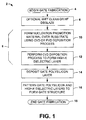
- an exemplary method 2 is illustrated for fabricating a transistor gate structure in accordance with one or more aspects of the present invention.
- the methods of the current invention involve the formation of a nucleation promotion layer on a semiconductor body or interface layer in order to enhance nucleation site density and thereby reduce surface roughness or non-uniformity in high-k dielectric material deposited over the nucleation promotion layer.
- the exemplary method 2 and other methods herein are illustrated and described below as a series of acts or events, it will be appreciated that the present invention is not limited by the illustrated ordering of such acts or events. For example, some acts may occur in different orders and/or concurrently with other acts or events apart from those illustrated and/or described herein, in accordance with the invention.
- Gate fabrication in the method 2 begins at 4, where a wet clean or HF deglaze operation may optionally be performed at 6 to remove any thin dielectric layers from the semiconductor body, such as silicon oxide (SiO), silicon nitride (SiN), or silicon oxynitride (SiON).
- a wet clean or HF deglaze operation may optionally be performed at 6 to remove any thin dielectric layers from the semiconductor body, such as silicon oxide (SiO), silicon nitride (SiN), or silicon oxynitride (SiON).
- wet cleaning operations can be performed at 6, or a dilute HF solution may be employed to deglaze the semiconductor body.
- a dilute HF solution may be employed to deglaze the semiconductor body.
- a dry process is employed comprising a mixture of anhydrous HF and isopropyl-alcohol to remove SiO.
- a gate dielectric is then processed at 8, including forming a nucleation promotion layer over the semiconductor body at 10, where the nucleation promotion layer comprises a metal, a metal silicide, or a metal silicate.
- the nucleation promotion layer may be formed at 10 using any appropriate material deposition technique, such as PVD, CVD, or others.
- a high-k dielectric layer is formed at 12 over the nucleation promotion layer using a chemical vapor deposition process.
- the invention may be employed in association with CVD deposition of any high-k dielectric layer material at 12 to any desired thickness, such as 10-100 ⁇ , for example 20-25 ⁇ , where the nucleation promotion layer may be formed at 10 over a silicon or other semiconductor substrate or any type of semiconductor body.
- the high-k dielectric layer comprises a high-k oxide, oxynitride, or nitride, such as hafnium oxide (HfO 2 ), hafnium oxynitride (HfON), hafnium silicon oxynitride (HfSiON) or others.
- HfO 2 hafnium oxide
- HfON hafnium oxynitride
- HfSiON hafnium silicon oxynitride
- High-k materials which may be deposited in association with the present invention may include, but are not limited to binary metal oxides including aluminum oxide (Al 2 O 3 ), zirconium oxide (ZrO 2 ), hafnium oxide (HfO 2 ), lanthanum oxide (La 2 O 3 ), yttrium oxide (Y 2 O 3 ), titanium oxide (TiO 2 ), as well as their silicates and aluminates; metal oxynitrides including aluminum oxynitride (AION), zirconium oxynitride (ZrON), hafnium oxynitride (HfON), lanthanum oxynitride (LaON), yttrium oxynitride (YON), as well as their silicates and aluminates such as ZrSiON, HfSiON, LaSiON, YsiON etc.; and perovskite-type oxides including a titanate system material such as barium titanate, strontium titan
- a gate contact layer such as metal, polysilicon, or equivalent, is then deposited at 14 over the high-k dielectric layer, and the gate contact layer and the high-k dielectric layer are patterned using any appropriate photolithographic techniques (e.g. , patterned etching, etc.) at 16 to form a gate structure, before the gate fabrication method 2 ends at 18.
- the method 2 facilitates reduction in the amount of roughness at the upper surface of the high-k dielectric material, which in turn facilitates EOT scaling, gate leakage current reduction, and increased device reliability through improved uniformity in electrical and material properties.
- the nucleation promotion layer formed at 10 may comprise any metal, metal silicate, or metal silicide in accordance with the present invention.
- the nucleation promotion layer preferably comprises the metal, a silicide of the metal, or a silicate of the metal.
- the nucleation promotion layer preferably comprises hafnium, a silicide of hafnium, or a silicate of hafnium.
- the employment of the same metal constituent in the nucleation promotion and high-k dielectric layers is believed to further enhance uniform nucleation of high-k precursor molecules, particularly in the initial stages of CVD deposition at 12, whereby upper surface roughness is reduced in the deposited high-k dielectric layer.
- the nucleation promotion layer is preferably thin, such as having a thickness of about 10 ⁇ or less.
- the nucleation promotion layer formed at 10 is a monolayer, for example, having an average thickness on the order of one or a few ⁇ .
- the nucleation promotion layer is a sub-monolayer.
- a sub-monolayer need not cover the entire surface of the semiconductor body.
- the sub-monolayer implementation does not provide nucleation promoting metal, metal silicide, or metal silicate over every portion of the semiconductor surface, the provision of some such molecules on the semiconductor body surface at 10 increases the nucleation site density and hence advantageously improves the nucleation of high-k material in the subsequent CVD high-k deposition at 12.
- the nucleation promotion layer may be formed at 10 using any appropriate material deposition technique, such as PVD, CVD, or others.
- the nucleation promotion layer and the high-k dielectric layer are both formed by CVD processing in-situ in a single chemical vapor deposition process chamber at 10 and 12.
- process pressures in the range of single digit mTorr up to tens of Torr may be employed, with lower pressure being preferable to facilitate control of the deposited material flux to the surface.
- One example is performed in an inert environment or an oxidizing environment (e.g. , Ar or Ar with O), and other implementations employ a reducing environment, such as hydrogen, ammonia, etc.
- a first step may employ essentially the same or similar process conditions at 10 as used for the bulk high-k deposition process at 12, but including only a hafnium precursor, for example, at 10.
- the process step at 10 may be continued to form a sub-monolayer, monolayer, or a thin film.
- a reducing or an oxidizing ambient may be provided (e.g. , by co-flowing appropriate hydrogen, ammonia, oxygen, etc.) to clean away all the ligands present on the precursor.
- the nucleation promotion layer is formed by PVD sputter processing at 10 using process pressures in the mTorr range using relatively low RF power, such as less than 100 W across an 8 inch wafer ( e.g. , power density of about 324 W/cm 2 or less) using an Ar process gas for sputtering a hafnium target.
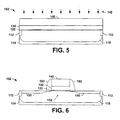
- an exemplary semiconductor device 102 is illustrated undergoing processing at various stages of manufacturing in accordance with various aspects of the invention, wherein the structures illustrated herein are not necessarily drawn to scale.
- the device 102 is illustrated comprising a wafer having a semiconductor body 104 therein, such as a silicon substrate or a layer of silicon overlying an insulator in an SOl device wafer, wherein the exemplary semiconductor body 104 is a lightly doped p-type silicon substrate.
- STI isolation structures 112 e.g. , SiO 2 are formed in the body 104 via an isolation process 114, which separate and provide electrical isolation between active areas, although other isolation structures may be provided, for example, using LOCOS techniques as are known.
- One or more p and/or n-type wells are then formed in the semiconductor body 104, including an n-well 118, and an optional wet clean or HF deglaze operation 116 may be performed to clean the top surface of the semiconductor body 104.
- an intentional interface layer (not shown) may optionally be formed over the semiconductor body 104 via any appropriate process steps before nucleation layer deposition.
- a PVD, CVD or other deposition process 122 is performed to deposit a thin nucleation promotion layer 120 comprising a metal, a metal silicide, or a metal silicate over all or a portion of the upper surface of the semiconductor body 104 (e.g., or over any intentional interface layer or layers, not shown).
- the nucleation promotion layer 120 is a thin hafnium film with a thickness less than about 10 ⁇ .
- Other examples include formation of a nucleation promotion monolayer 120, for example, having an average thickness on the order of one or a few ⁇ .
- the nucleation promotion layer 120 is a sub-monolayer, which need not cover the entire surface of the semiconductor body 104.
- a high-k dielectric layer 130 is deposited over the nucleation promotion layer 120 via a CVD deposition process 132 as described above, wherein the processes 122 and 132 may, but need not, be performed in-situ in a single CVD process chamber or tool.
- the high-k dielectric layer 130 comprises any appropriate high-k dielectric material, such as those mentioned above, formed to any desired thickness, such as 10-100 ⁇ , for example 20-25 ⁇ .
- a gate contact layer 140 such as metal, polysilicon or equivalent is deposited over the high-k material 130 via a deposition process 142. As illustrated in Fig. 5, the gate contact layer 140 and the high-k dielectric layer 130 are then patterned to form a transistor gate structure. Source/drain regions 150 are doped with p-type impurities on either side of a channel region 152 in the semiconductor body 104, and sidewall spacers 160 are formed along the sides of the patterned layers 120, 130, and 140 as illustrated in Fig. 8. Thereafter, interconnect processing (not shown) is performed to interconnect the illustrated MOS type transistor and other electrical components in the device 102.
- interconnect processing (not shown) is performed to interconnect the illustrated MOS type transistor and other electrical components in the device 102.
- FIG. 7 another aspect of the invention provides methods for fabricating a transistor gate structure, in which an intentional interface layer is formed over the semiconductor body, and a nucleation promotion layer is formed over the intentional interface layer prior to deposition of high-k gate dielectric material.
- the inventors have appreciated that forming a nucleation promotion layer over the intentional interface layer provides an increased number or higher density of nucleation sites for deposition of high-k material, thereby promoting uniform formation of high-k dielectric material without the degree of upper surface roughness found in conventional CVD processes.
- An exemplary method 202 is illustrated in Fig. 7 in accordance with this aspect of the invention.
- an intentional interface layer is formed at 206 over a substrate or other semiconductor body, using any appropriate materials and deposition or thermal growth techniques as are known. Moreover, the intentional interface may be formed to any desired thickness at 206 in accordance with the present invention.
- a gate dielectric is then created at 208 by forming a nucleation promotion layer over the semiconductor body at 210 and depositing high-k material using a CVD deposition process at 212.
- the nucleation promotion layer formed comprises a metal, a metal silicide, or a metal silicate, which may be formed at 210 using any appropriate material deposition technique, such as PVD, CVD, or others.
- the high-k dielectric layer comprises a high-k oxide, oxynitride, or nitride, such as hafnium oxide (HfO 2 ), hafnium oxynitride (HfON), hafnium silicon oxynitride (HfSiON) or others, although any of the above-mentioned high-k materials may be employed at 212.
- HfO 2 hafnium oxide
- HfON hafnium oxynitride
- HfSiON hafnium silicon oxynitride
- a gate contact layer such as metal, polysilicon, or equivalent, is then deposited at 214 over the high-k dielectric layer, and the gate contact layer and the high-k dielectric layer are patterned using any appropriate photolithographic techniques at 216 to form a gate structure, before the gate fabrication method 202 ends at 218.
- the exemplary method 202 facilitates reduction in the amount of roughness at the upper surface of the high-k dielectric material, which in turn facilitates EOT scaling, gate leakage current reduction, and increased device reliability through improved uniformity in electrical and material properties.
- the nucleation promotion layer formed at 210 may comprise any metal, metal silicate, or metal silicide in accordance with the present invention.
- the nucleation promotion layer preferably comprises the same metal, a silicide of the metal, or a silicate of the metal.
- the nucleation promotion layer preferably comprises hafnium, a silicide of hafnium, or a silicate of hafnium.
- the nucleation promotion layer is preferably thin, such as having a thickness of about 10 ⁇ or less.
- the nucleation promotion layer formed at 210 is a monolayer, for example, having an average thickness on the order of one or a few ⁇ .
- the nucleation promotion layer is a sub-monolayer.
- the nucleation promotion layer may be formed at 210 using any appropriate material deposition technique, such as PVD, CVD, or others.
- the nucleation promotion layer and the high-k dielectric layer are formed at 210 and 212 by CVD processing in-situ in a single chemical vapor deposition process chamber, such as using the process conditions described above.
Landscapes
- Insulated Gate Type Field-Effect Transistor (AREA)
- Thin Film Transistor (AREA)
- Formation Of Insulating Films (AREA)
Abstract
Description
Claims (9)
- A method of fabricating a transistor gate structure, comprising:forming a nucleation promotion layer over a semiconductor body, the nucleation promotion layer comprising a metal, a metal silicide, or a metal silicate;forming a high-k dielectric layer over the nucleation promotion layer using a chemical vapor deposition process;forming a gate contact layer over the high-k dielectric layer; andpatterning the gate contact layer and the high-k dielectric layer.
- The method of claim 1, wherein the nucleation promotion layer has a thickness of about 10 Å or less.
- The method of claim 2, wherein the nucleation promotion layer is a monolayer.
- The method of claim 2, wherein the nucleation promotion layer is a sub-monolayer.
- The method of any one of claims 1 to 3, wherein forming the nucleation promotion layer and forming the high-k dielectric layer are performed in-situ in a single chemical vapor deposition process chamber.
- The method of any one of claims 1 to 4, wherein forming the nucleation promotion layer comprises performing one of a chemical vapor deposition process and a physical vapor deposition process.
- The method of any one of claims 1 to 6, wherein the high-k dielectric layer is a compound material comprising a metal, and wherein the nucleation promotion layer comprises the metal, a silicide of the metal, or a silicate of the metal.
- The method of claim 7, wherein the metal is hafnium.
- A method of fabricating a transistor gate structure, comprising:forming at least one intentional interface layer over a semiconductor body;forming a nucleation promotion layer over the intentional interface layer, the nucleation promotion layer comprising a metal, a metal silicide, or a metal silicate;forming a high-k dielectric layer over the nucleation promotion layer using a chemical vapor deposition process;forming a gate contact layer over the high-k dielectric layer; andpatterning the gate contact layer and the high-k dielectric layer.
Applications Claiming Priority (2)
| Application Number | Priority Date | Filing Date | Title |
|---|---|---|---|
| US335557 | 1989-04-10 | ||
| US10/335,557 US6762114B1 (en) | 2002-12-31 | 2002-12-31 | Methods for transistor gate fabrication and for reducing high-k gate dielectric roughness |
Publications (2)
| Publication Number | Publication Date |
|---|---|
| EP1435649A2 true EP1435649A2 (en) | 2004-07-07 |
| EP1435649A3 EP1435649A3 (en) | 2005-01-05 |
Family
ID=32507394
Family Applications (1)
| Application Number | Title | Priority Date | Filing Date |
|---|---|---|---|
| EP03104979A Withdrawn EP1435649A3 (en) | 2002-12-31 | 2003-12-24 | Methods of forming a transistor gate |
Country Status (3)
| Country | Link |
|---|---|
| US (1) | US6762114B1 (en) |
| EP (1) | EP1435649A3 (en) |
| JP (1) | JP2004214661A (en) |
Families Citing this family (30)
| Publication number | Priority date | Publication date | Assignee | Title |
|---|---|---|---|---|
| US8026161B2 (en) | 2001-08-30 | 2011-09-27 | Micron Technology, Inc. | Highly reliable amorphous high-K gate oxide ZrO2 |
| US6767795B2 (en) * | 2002-01-17 | 2004-07-27 | Micron Technology, Inc. | Highly reliable amorphous high-k gate dielectric ZrOXNY |
| US7589029B2 (en) | 2002-05-02 | 2009-09-15 | Micron Technology, Inc. | Atomic layer deposition and conversion |
| US7160577B2 (en) | 2002-05-02 | 2007-01-09 | Micron Technology, Inc. | Methods for atomic-layer deposition of aluminum oxides in integrated circuits |
| US7221586B2 (en) | 2002-07-08 | 2007-05-22 | Micron Technology, Inc. | Memory utilizing oxide nanolaminates |
| US7192892B2 (en) * | 2003-03-04 | 2007-03-20 | Micron Technology, Inc. | Atomic layer deposited dielectric layers |
| CN100352017C (en) * | 2003-03-17 | 2007-11-28 | 富士通株式会社 | Semiconductor device and method for manufacturing semiconductor device |
| US7135369B2 (en) | 2003-03-31 | 2006-11-14 | Micron Technology, Inc. | Atomic layer deposited ZrAlxOy dielectric layers including Zr4AlO9 |
| US7183186B2 (en) | 2003-04-22 | 2007-02-27 | Micro Technology, Inc. | Atomic layer deposited ZrTiO4 films |
| US7049192B2 (en) * | 2003-06-24 | 2006-05-23 | Micron Technology, Inc. | Lanthanide oxide / hafnium oxide dielectrics |
| US7258895B2 (en) * | 2003-08-06 | 2007-08-21 | Micron Technology, Inc. | Methods of forming material on a substrate, and a method of forming a field effect transistor gate oxide on a substrate |
| US7115530B2 (en) * | 2003-12-03 | 2006-10-03 | Texas Instruments Incorporated | Top surface roughness reduction of high-k dielectric materials using plasma based processes |
| US7588988B2 (en) | 2004-08-31 | 2009-09-15 | Micron Technology, Inc. | Method of forming apparatus having oxide films formed using atomic layer deposition |
| US7235501B2 (en) | 2004-12-13 | 2007-06-26 | Micron Technology, Inc. | Lanthanum hafnium oxide dielectrics |
| US7560395B2 (en) | 2005-01-05 | 2009-07-14 | Micron Technology, Inc. | Atomic layer deposited hafnium tantalum oxide dielectrics |
| US7662729B2 (en) | 2005-04-28 | 2010-02-16 | Micron Technology, Inc. | Atomic layer deposition of a ruthenium layer to a lanthanide oxide dielectric layer |
| US7927948B2 (en) | 2005-07-20 | 2011-04-19 | Micron Technology, Inc. | Devices with nanocrystals and methods of formation |
| US8110469B2 (en) | 2005-08-30 | 2012-02-07 | Micron Technology, Inc. | Graded dielectric layers |
| US7410910B2 (en) | 2005-08-31 | 2008-08-12 | Micron Technology, Inc. | Lanthanum aluminum oxynitride dielectric films |
| US20070066021A1 (en) | 2005-09-16 | 2007-03-22 | Texas Instruments Inc. | Formation of gate dielectrics with uniform nitrogen distribution |
| US7972974B2 (en) | 2006-01-10 | 2011-07-05 | Micron Technology, Inc. | Gallium lanthanide oxide films |
| US7709402B2 (en) | 2006-02-16 | 2010-05-04 | Micron Technology, Inc. | Conductive layers for hafnium silicon oxynitride films |
| JP4868910B2 (en) * | 2006-03-30 | 2012-02-01 | 株式会社東芝 | Semiconductor device and manufacturing method thereof |
| US7759747B2 (en) | 2006-08-31 | 2010-07-20 | Micron Technology, Inc. | Tantalum aluminum oxynitride high-κ dielectric |
| US7544604B2 (en) | 2006-08-31 | 2009-06-09 | Micron Technology, Inc. | Tantalum lanthanide oxynitride films |
| US7432548B2 (en) | 2006-08-31 | 2008-10-07 | Micron Technology, Inc. | Silicon lanthanide oxynitride films |
| US7605030B2 (en) | 2006-08-31 | 2009-10-20 | Micron Technology, Inc. | Hafnium tantalum oxynitride high-k dielectric and metal gates |
| US7563730B2 (en) | 2006-08-31 | 2009-07-21 | Micron Technology, Inc. | Hafnium lanthanide oxynitride films |
| US7776765B2 (en) | 2006-08-31 | 2010-08-17 | Micron Technology, Inc. | Tantalum silicon oxynitride high-k dielectrics and metal gates |
| US8962078B2 (en) | 2012-06-22 | 2015-02-24 | Tokyo Electron Limited | Method for depositing dielectric films |
Family Cites Families (27)
| Publication number | Priority date | Publication date | Assignee | Title |
|---|---|---|---|---|
| JPS5861763A (en) * | 1981-10-09 | 1983-04-12 | 武笠 均 | Feel sensor fire fighting apparatus |
| US6320238B1 (en) | 1996-12-23 | 2001-11-20 | Agere Systems Guardian Corp. | Gate structure for integrated circuit fabrication |
| US6063698A (en) * | 1997-06-30 | 2000-05-16 | Motorola, Inc. | Method for manufacturing a high dielectric constant gate oxide for use in semiconductor integrated circuits |
| US6020243A (en) * | 1997-07-24 | 2000-02-01 | Texas Instruments Incorporated | Zirconium and/or hafnium silicon-oxynitride gate dielectric |
| US6451677B1 (en) | 1998-02-23 | 2002-09-17 | Texas Instruments Incorporated | Plasma-enhanced chemical vapor deposition of a nucleation layer in a tungsten metallization process |
| US6251761B1 (en) | 1998-11-24 | 2001-06-26 | Texas Instruments Incorporated | Process for polycrystalline silicon gates and high-K dielectric compatibility |
| US6303940B1 (en) | 1999-01-26 | 2001-10-16 | Agere Systems Guardian Corp. | Charge injection transistor using high-k dielectric barrier layer |
| US6060755A (en) * | 1999-07-19 | 2000-05-09 | Sharp Laboratories Of America, Inc. | Aluminum-doped zirconium dielectric film transistor structure and deposition method for same |
| US6297539B1 (en) * | 1999-07-19 | 2001-10-02 | Sharp Laboratories Of America, Inc. | Doped zirconia, or zirconia-like, dielectric film transistor structure and deposition method for same |
| US6207584B1 (en) * | 2000-01-05 | 2001-03-27 | International Business Machines Corp. | High dielectric constant material deposition to achieve high capacitance |
| US6448127B1 (en) | 2000-01-14 | 2002-09-10 | Advanced Micro Devices, Inc. | Process for formation of ultra-thin base oxide in high k/oxide stack gate dielectrics of mosfets |
| US6407435B1 (en) | 2000-02-11 | 2002-06-18 | Sharp Laboratories Of America, Inc. | Multilayer dielectric stack and method |
| US6271094B1 (en) | 2000-02-14 | 2001-08-07 | International Business Machines Corporation | Method of making MOSFET with high dielectric constant gate insulator and minimum overlap capacitance |
| KR20020094026A (en) * | 2000-05-09 | 2002-12-16 | 모토로라 인코포레이티드 | Amorphous metal oxide gate dielectric structure and method thereof |
| US6184072B1 (en) | 2000-05-17 | 2001-02-06 | Motorola, Inc. | Process for forming a high-K gate dielectric |
| US6444592B1 (en) | 2000-06-20 | 2002-09-03 | International Business Machines Corporation | Interfacial oxidation process for high-k gate dielectric process integration |
| US6380104B1 (en) | 2000-08-10 | 2002-04-30 | Taiwan Semiconductor Manufacturing Company | Method for forming composite gate dielectric layer equivalent to silicon oxide gate dielectric layer |
| US6495474B1 (en) * | 2000-09-11 | 2002-12-17 | Agere Systems Inc. | Method of fabricating a dielectric layer |
| US6939816B2 (en) | 2000-11-10 | 2005-09-06 | Texas Instruments Incorporated | Method to improve the uniformity and reduce the surface roughness of the silicon dielectric interface |
| US6927435B2 (en) * | 2001-01-16 | 2005-08-09 | Renesas Technology Corp. | Semiconductor device and its production process |
| US6524651B2 (en) * | 2001-01-26 | 2003-02-25 | Battelle Memorial Institute | Oxidized film structure and method of making epitaxial metal oxide structure |
| US6844604B2 (en) * | 2001-02-02 | 2005-01-18 | Samsung Electronics Co., Ltd. | Dielectric layer for semiconductor device and method of manufacturing the same |
| US6514828B2 (en) * | 2001-04-20 | 2003-02-04 | Micron Technology, Inc. | Method of fabricating a highly reliable gate oxide |
| US6709989B2 (en) * | 2001-06-21 | 2004-03-23 | Motorola, Inc. | Method for fabricating a semiconductor structure including a metal oxide interface with silicon |
| US6511925B1 (en) * | 2001-10-19 | 2003-01-28 | Lsi Logic Corporation | Process for forming high dielectric constant gate dielectric for integrated circuit structure |
| US6455330B1 (en) | 2002-01-28 | 2002-09-24 | Taiwan Semiconductor Manufacturing Company | Methods to create high-k dielectric gate electrodes with backside cleaning |
| US7449385B2 (en) * | 2002-07-26 | 2008-11-11 | Texas Instruments Incorporated | Gate dielectric and method |
-
2002
- 2002-12-31 US US10/335,557 patent/US6762114B1/en not_active Expired - Lifetime
-
2003
- 2003-12-24 EP EP03104979A patent/EP1435649A3/en not_active Withdrawn
- 2003-12-25 JP JP2003429603A patent/JP2004214661A/en not_active Abandoned
Also Published As
| Publication number | Publication date |
|---|---|
| EP1435649A3 (en) | 2005-01-05 |
| US20040127003A1 (en) | 2004-07-01 |
| JP2004214661A (en) | 2004-07-29 |
| US6762114B1 (en) | 2004-07-13 |
Similar Documents
| Publication | Publication Date | Title |
|---|---|---|
| US6762114B1 (en) | Methods for transistor gate fabrication and for reducing high-k gate dielectric roughness | |
| US6852645B2 (en) | High temperature interface layer growth for high-k gate dielectric | |
| US20040126944A1 (en) | Methods for forming interfacial layer for deposition of high-k dielectrics | |
| US7385265B2 (en) | High dielectric constant MOSFET device | |
| US6809370B1 (en) | High-k gate dielectric with uniform nitrogen profile and methods for making the same | |
| US6979623B2 (en) | Method for fabricating split gate transistor device having high-k dielectrics | |
| US7091119B2 (en) | Encapsulated MOS transistor gate structures and methods for making the same | |
| JP4002868B2 (en) | Dual gate structure and method of manufacturing integrated circuit having dual gate structure | |
| CN100416859C (en) | Method of forming metal/high-k gate stack with high mobility | |
| US8802519B2 (en) | Work function adjustment with the implant of lanthanides | |
| US20040070036A1 (en) | ULSI MOS with high dielectric constant gate insulator | |
| US9418853B1 (en) | Method for forming a stacked layer structure | |
| JPH11135774A (en) | High dielectric constant silicate gate dielectric | |
| JP4120938B2 (en) | Semiconductor device having high dielectric constant insulating film and manufacturing method thereof | |
| US7045431B2 (en) | Method for integrating high-k dielectrics in transistor devices | |
| US8633119B2 (en) | Methods for manufacturing high dielectric constant films | |
| US20120289052A1 (en) | Methods for Manufacturing High Dielectric Constant Films | |
| KR100598051B1 (en) | Manufacturing method of semiconductor device | |
| EP1863072A1 (en) | Method for modulating the effective work function | |
| US20250081498A1 (en) | Semiconductor structure | |
| US20060234436A1 (en) | Method of forming a semiconductor device having a high-k dielectric | |
| TW201301511A (en) | Metal gate and fabrication method thereof | |
| TWI473172B (en) | Metal gate with zirconium | |
| US20070232078A1 (en) | In situ processing for ultra-thin gate oxide scaling |
Legal Events
| Date | Code | Title | Description |
|---|---|---|---|
| PUAI | Public reference made under article 153(3) epc to a published international application that has entered the european phase |
Free format text: ORIGINAL CODE: 0009012 |
|
| AK | Designated contracting states |
Kind code of ref document: A2 Designated state(s): AT BE BG CH CY CZ DE DK EE ES FI FR GB GR HU IE IT LI LU MC NL PT RO SE SI SK TR |
|
| AX | Request for extension of the european patent |
Extension state: AL LT LV MK |
|
| PUAL | Search report despatched |
Free format text: ORIGINAL CODE: 0009013 |
|
| AK | Designated contracting states |
Kind code of ref document: A3 Designated state(s): AT BE BG CH CY CZ DE DK EE ES FI FR GB GR HU IE IT LI LU MC NL PT RO SE SI SK TR |
|
| AX | Request for extension of the european patent |
Extension state: AL LT LV MK |
|
| RIC1 | Information provided on ipc code assigned before grant |
Ipc: 7H 01L 21/28 B Ipc: 7H 01L 29/51 B Ipc: 7H 01L 21/336 A |
|
| AKX | Designation fees paid | ||
| REG | Reference to a national code |
Ref country code: DE Ref legal event code: 8566 |
|
| STAA | Information on the status of an ep patent application or granted ep patent |
Free format text: STATUS: THE APPLICATION IS DEEMED TO BE WITHDRAWN |
|
| 18D | Application deemed to be withdrawn |
Effective date: 20050606 |