EP1435648A1 - Process of making CMOS and drain extension MOS transistors with silicided gate - Google Patents
Process of making CMOS and drain extension MOS transistors with silicided gate Download PDFInfo
- Publication number
- EP1435648A1 EP1435648A1 EP02425807A EP02425807A EP1435648A1 EP 1435648 A1 EP1435648 A1 EP 1435648A1 EP 02425807 A EP02425807 A EP 02425807A EP 02425807 A EP02425807 A EP 02425807A EP 1435648 A1 EP1435648 A1 EP 1435648A1
- Authority
- EP
- European Patent Office
- Prior art keywords
- layer
- substrate
- forming
- drain
- low
- Prior art date
- Legal status (The legal status is an assumption and is not a legal conclusion. Google has not performed a legal analysis and makes no representation as to the accuracy of the status listed.)
- Withdrawn
Links
Images


Classifications
-
- H—ELECTRICITY
- H10—SEMICONDUCTOR DEVICES; ELECTRIC SOLID-STATE DEVICES NOT OTHERWISE PROVIDED FOR
- H10D—INORGANIC ELECTRIC SEMICONDUCTOR DEVICES
- H10D30/00—Field-effect transistors [FET]
- H10D30/01—Manufacture or treatment
- H10D30/021—Manufacture or treatment of FETs having insulated gates [IGFET]
- H10D30/0223—Manufacture or treatment of FETs having insulated gates [IGFET] having source and drain regions or source and drain extensions self-aligned to sides of the gate
- H10D30/0227—Manufacture or treatment of FETs having insulated gates [IGFET] having source and drain regions or source and drain extensions self-aligned to sides of the gate having both lightly-doped source and drain extensions and source and drain regions self-aligned to the sides of the gate, e.g. lightly-doped drain [LDD] MOSFET or double-diffused drain [DDD] MOSFET
-
- H—ELECTRICITY
- H10—SEMICONDUCTOR DEVICES; ELECTRIC SOLID-STATE DEVICES NOT OTHERWISE PROVIDED FOR
- H10D—INORGANIC ELECTRIC SEMICONDUCTOR DEVICES
- H10D30/00—Field-effect transistors [FET]
- H10D30/01—Manufacture or treatment
- H10D30/021—Manufacture or treatment of FETs having insulated gates [IGFET]
- H10D30/0221—Manufacture or treatment of FETs having insulated gates [IGFET] having asymmetry in the channel direction, e.g. lateral high-voltage MISFETs having drain offset region or extended-drain MOSFETs [EDMOS]
-
- H—ELECTRICITY
- H10—SEMICONDUCTOR DEVICES; ELECTRIC SOLID-STATE DEVICES NOT OTHERWISE PROVIDED FOR
- H10D—INORGANIC ELECTRIC SEMICONDUCTOR DEVICES
- H10D30/00—Field-effect transistors [FET]
- H10D30/60—Insulated-gate field-effect transistors [IGFET]
- H10D30/601—Insulated-gate field-effect transistors [IGFET] having lightly-doped drain or source extensions, e.g. LDD IGFETs or DDD IGFETs
- H10D30/603—Insulated-gate field-effect transistors [IGFET] having lightly-doped drain or source extensions, e.g. LDD IGFETs or DDD IGFETs having asymmetry in the channel direction, e.g. lateral high-voltage MISFETs having drain offset region or extended drain IGFETs [EDMOS]
-
- H—ELECTRICITY
- H10—SEMICONDUCTOR DEVICES; ELECTRIC SOLID-STATE DEVICES NOT OTHERWISE PROVIDED FOR
- H10D—INORGANIC ELECTRIC SEMICONDUCTOR DEVICES
- H10D84/00—Integrated devices formed in or on semiconductor substrates that comprise only semiconducting layers, e.g. on Si wafers or on GaAs-on-Si wafers
- H10D84/01—Manufacture or treatment
- H10D84/0123—Integrating together multiple components covered by H10D12/00 or H10D30/00, e.g. integrating multiple IGBTs
- H10D84/0126—Integrating together multiple components covered by H10D12/00 or H10D30/00, e.g. integrating multiple IGBTs the components including insulated gates, e.g. IGFETs
- H10D84/0165—Integrating together multiple components covered by H10D12/00 or H10D30/00, e.g. integrating multiple IGBTs the components including insulated gates, e.g. IGFETs the components including complementary IGFETs, e.g. CMOS devices
- H10D84/017—Manufacturing their source or drain regions, e.g. silicided source or drain regions
-
- H—ELECTRICITY
- H10—SEMICONDUCTOR DEVICES; ELECTRIC SOLID-STATE DEVICES NOT OTHERWISE PROVIDED FOR
- H10D—INORGANIC ELECTRIC SEMICONDUCTOR DEVICES
- H10D84/00—Integrated devices formed in or on semiconductor substrates that comprise only semiconducting layers, e.g. on Si wafers or on GaAs-on-Si wafers
- H10D84/01—Manufacture or treatment
- H10D84/0123—Integrating together multiple components covered by H10D12/00 or H10D30/00, e.g. integrating multiple IGBTs
- H10D84/0126—Integrating together multiple components covered by H10D12/00 or H10D30/00, e.g. integrating multiple IGBTs the components including insulated gates, e.g. IGFETs
- H10D84/0165—Integrating together multiple components covered by H10D12/00 or H10D30/00, e.g. integrating multiple IGBTs the components including insulated gates, e.g. IGFETs the components including complementary IGFETs, e.g. CMOS devices
- H10D84/0172—Manufacturing their gate conductors
- H10D84/0174—Manufacturing their gate conductors the gate conductors being silicided
-
- H—ELECTRICITY
- H10—SEMICONDUCTOR DEVICES; ELECTRIC SOLID-STATE DEVICES NOT OTHERWISE PROVIDED FOR
- H10D—INORGANIC ELECTRIC SEMICONDUCTOR DEVICES
- H10D84/00—Integrated devices formed in or on semiconductor substrates that comprise only semiconducting layers, e.g. on Si wafers or on GaAs-on-Si wafers
- H10D84/01—Manufacture or treatment
- H10D84/02—Manufacture or treatment characterised by using material-based technologies
- H10D84/03—Manufacture or treatment characterised by using material-based technologies using Group IV technology, e.g. silicon technology or silicon-carbide [SiC] technology
- H10D84/038—Manufacture or treatment characterised by using material-based technologies using Group IV technology, e.g. silicon technology or silicon-carbide [SiC] technology using silicon technology, e.g. SiGe
-
- H—ELECTRICITY
- H10—SEMICONDUCTOR DEVICES; ELECTRIC SOLID-STATE DEVICES NOT OTHERWISE PROVIDED FOR
- H10D—INORGANIC ELECTRIC SEMICONDUCTOR DEVICES
- H10D64/00—Electrodes of devices having potential barriers
- H10D64/01—Manufacture or treatment
- H10D64/013—Manufacture or treatment of electrodes having a conductor capacitively coupled to a semiconductor by an insulator
- H10D64/01302—Manufacture or treatment of electrodes having a conductor capacitively coupled to a semiconductor by an insulator the insulator being formed after the semiconductor body, the semiconductor being silicon
- H10D64/01304—Manufacture or treatment of electrodes having a conductor capacitively coupled to a semiconductor by an insulator the insulator being formed after the semiconductor body, the semiconductor being silicon characterised by the conductor
- H10D64/01318—Manufacture or treatment of electrodes having a conductor capacitively coupled to a semiconductor by an insulator the insulator being formed after the semiconductor body, the semiconductor being silicon characterised by the conductor the conductor comprising a layer of alloy material, compound material or organic material contacting the insulator, e.g. TiN
- H10D64/0132—Manufacture or treatment of electrodes having a conductor capacitively coupled to a semiconductor by an insulator the insulator being formed after the semiconductor body, the semiconductor being silicon characterised by the conductor the conductor comprising a layer of alloy material, compound material or organic material contacting the insulator, e.g. TiN the conductor being a metallic silicide
Definitions
- the present invention relates to a process for forming, on a common semiconductor substrate, a number of components, among which CMOS transistors, vertical or lateral drain-extension MOS transistors, and LDMOS (Lateral Double-diffused MOS) transistors, in particular by dedicated silicidation techniques.
- CMOS transistors vertical or lateral drain-extension MOS transistors
- LDMOS Layer Double-diffused MOS
- the invention relates to a process for forming, on a common semiconductor substrate, CMOS transistors and drain-extension MOS transistors on at least first and second substrate portions, respectively, the process comprising the following steps:
- the invention relates, in particular, to a process for forming CMOS transistors by a self-aligned silicidation technique to form source and drain active areas and low-resistance polysilicon gate electrodes, and for forming drain-extension MOS transistors with a gate region which is silicided by means of a different technique.
- CMOS transistors by a self-aligned silicidation technique to form source and drain active areas and low-resistance polysilicon gate electrodes
- drain-extension MOS transistors with a gate region which is silicided by means of a different technique.
- MOS transistor 1 comprising a substrate 1, e.g. of the P + type, on which an epitaxial layer 2, of the same species as the substrate but less doped, is formed.
- a first N + surface region 4 is formed between the epitaxial layer 2 and the sinker region 3.
- a second N + region 5 is formed in the substrate 1.
- a third, lightly doped N - region 6 is formed between the first and second region.
- the third region 6 lies adjacent to the second region 5, but out of contact with the first region 4.
- the third, lightly doped N- region 6 provides the drift region for the drain-extension MOS transistor.
- a gate electrode G is formed on the layer 2, between the first and third regions 4 and 6, the electrode G being isolated by means of an oxide layer 7.
- the gate electrode G comprises a polysilicon layer 8 overlain by a silicide layer 9.
- the drain-extension MOS device is provided with contacts 10, 11 and 12 to drain, body and source regions, respectively.
- the source contact 12 may be either provided on the back side of the substrate 1, as shown in Figure 1, or on the body contact 11.
- Drain-extension MOS devices for RF applications further require a short gate electrode G but with low resistance, thus capped with a silicide layer 9, so that devices having a high cutoff frequency (Ft) can be obtained, which reach a high oscillation frequency (fmax).
- Ft cutoff frequency
- fmax high oscillation frequency
- a prior method for integrating CMOS transistors and drain-extension MOS transistors on the same substrate comprises additional steps for forming the MOS devices.
- standard dielectrics s deposited and patterned to protect the drift region from the standard silicidation technique.
- this first method has a drawback in that it significantly increases the resistivity of the gate electrode by reason of the protective layers that overlie the gate electrode reducing the amount of area that has to be covered with a silicide layer.
- the underlying technical problem of this invention is to provide a process for integrating CMOS and drain-extension MOS devices, having appropriate structural and functional features so as to optimize the performance of the individual devices, thereby overcoming the limitations of prior art devices.
- the resolvent idea on which this invention stands is a process which can be compatible with a standard VLSI CMOS process allowing to realize drain-extension MOS transistors having fully silicided gates and not silicised portions of adjacent lightly doped active regions
- the regions that are not to be silicided are screened off by means of layers already provided in the standard process for making CMOS devices.
- a first dielectric layer 14 and first semiconductor material layer 15 are provided on a semiconductor substrate S which includes a first portion A where CMOS devices are to be formed, a second portion B providing separation, and a third portion C where drain-extension MOS devices are to be formed.
- the first layer 16 is removed from the third portion C of the substrate 1 by a photolithographic operation followed by etching.
- the first dielectric layer 14 is an oxide layer from which the gate oxide layer of the CMOS transistors is formed
- the first layer 15 of semiconductor material is a polysilicon layer from which the layer POLY1 of the CMOS transistors is formed.
- a cascade formation, on the whole device, of a stack structure comprising a second dielectric layer 16, e.g. silicon oxide, a second semiconductor material layer 17, e.g. polysilicon, and a low-resistivity layer 18, e.g. comprising tungsten.
- a second dielectric layer 16 e.g. silicon oxide
- a second semiconductor material layer 17 e.g. polysilicon
- a low-resistivity layer 18 e.g. comprising tungsten.
- First openings 19 are provided in portion C, in both the semiconductor material layer 17 and low resistivity layer 18, to define a gate region 20 of the RF application devices.
- the second semiconductor material layer 17 and low-resistivity layer 18 are removed from portion A completely.
- the dielectric layer 16 formed on the first polysilicon layer 15 is utilized as a screen during removal of the second semiconductor material layer 17 in the portion C of the substrate 14.
- portion B which isolates the substrate portion A, where the CMOS devices are to be formed, from the substrate portion C where the RF application devices are to be formed.
- openings 22' are made to define gate regions 22 of the CMOS transistors in the portion A of the substrate 14, as shown in Figure 4.
- the substrate is then implanted with first LDD (Lightly Doped Drain) regions 23 to provide source and drain regions of the CMOS transistors.
- LDD Lightly Doped Drain
- drain regions 24 of the drain-extension MOS transistors are also formed during this process step.
- the drain region 24 includes a lightly doped drift region adjacent to the gate region 20.
- spacers 25 are then applied to form spacers 25 on the sidewalls of the gate regions 20 of the RF devices, and on those of the division structure 21 and the gate regions 22 of the CMOS transistors.
- second heavily doped implanted regions 26 are provided to complete the source and drain regions of the CMOS transistors, and the body and drain regions of the drain-extension MOS transistors.
- a protective layer 27 is deposited onto the whole device. This protective layer 27 is removed from the substrate portion A completely to expose the substrate S.
- the protective layer 27 is provided with openings 28 in the body and drain regions of the drain-extension MOS transistor.
- the protective layer 27 may be a dielectric layer.
- a metal layer is formed on the whole device. This metal layer may be formed with a transition metal.
- the device is then subjected to a thermal process, so that the metal layer reacts with the substrate which is not covered by the protective layer 27 and forms a silicide layer 29.
- a first dielectric layer 14a, first semiconductor material layer 15a, and second dielectric layer 16a, e.g. silicon oxide, are provided on a semiconductor substrate S which includes a first portion A, second portion B, and third portion C.
- the second dielectric layer 16a is removed from the third portion C of the substrate 1 where the RF devices are to be formed, and from a portion of the second portion B adjacent to the third portion C, by a photolithographic operation followed by etching.
- the first dielectric layer 14a is an oxide layer with which the gate oxide layer of the CMOS transistors and the drain-extension MOS transistors is formed
- the first layer 15a of semiconductor material is a polysilicon layer by means of which the layer POLY1 of the CMOS transistors and a first portion of the gate region of the drain-extension MOS transistor are formed.
- First openings 19a are provided in the portion C, in the first semiconductor material layer 16a, in the second semiconductor material layer 17a, and in the low resistivity layer 18a, to define a gate region 20a for the RF application devices.
- the second semiconductor material layer 17a and the low-resistivity layer 18 are fully removed from the substrate portion A where the CMOS devices are to be formed.
- the second dielectric layer 16a formed on the first polysilicon layer 15a is utilized as a screen during removal of the first and second semiconductor material layers 15a and 17a from the portion C of the substrate S to produce the ports 19a.
- a structure 21a is defined in portion B to isolate the substrate portion A where the CMOS devices are to be formed from the substrate portion C where the RF application devices are to be formed.
- gate regions 22a of the CMOS transistors are defined in the portion A of the substrate 14a, as shown in Figure 4.
- first LDD implanted regions 23a are then formed so as to provide source and drain regions for the CMOS transistors.
- drift regions 24a of the drain-extension MOS transistors are also formed during this process step.
- spacers 25a are then applied to form spacers 25a on the sidewalls of the gate regions 20a of the RF devices, and on those of the division structure 21a and the gate regions 22a of the CMOS transistors.
- second heavily doped implanted regions 26a are provided to complete the source and drain regions of the CMOS transistors, and to complete the body and drain regions of the drain-extension MOS transistors.
- a protective layer 27a is then deposited onto the whole device. This protective layer 27a is removed from the substrate portion A completely to expose the substrate S.
- the protective layer 27a is provided with openings 28a at the body and drain regions of the drain-extension MOS transistor.
- a metal layer is formed on the whole device.
- the device is then subjected to a thermal process so that the metal layer reacts with the uncovered substrate by the protective layer 27a and forms a silicide layer 29a.
- the method of the invention allows high-density high-performance CMOS structures to be integrated on a common substrate along with high- performance drain-extension MOS structures, without introducing any dedicated process steps to make either structures.
- the gate region 20 of the drain-extension MOS transistor is provided with a low-resistance layer 18 by depositing the low-resistance layer 18 onto the polysilicon layer 17, while the heavily doped regions 26 of the CMOS transistors and the drain-extension MOS transistors are silicided in a self-aligned silicidation process that will also silicide the gate regions 22 of the CMOS transistors.
Landscapes
- Metal-Oxide And Bipolar Metal-Oxide Semiconductor Integrated Circuits (AREA)
Abstract
Description
- The present invention relates to a process for forming, on a common semiconductor substrate, a number of components, among which CMOS transistors, vertical or lateral drain-extension MOS transistors, and LDMOS (Lateral Double-diffused MOS) transistors, in particular by dedicated silicidation techniques.
- Specifically, the invention relates to a process for forming, on a common semiconductor substrate, CMOS transistors and drain-extension MOS transistors on at least first and second substrate portions, respectively, the process comprising the following steps:
- in said first portion, forming at least one CMOS transistor having a first gate region projecting from the substrate, and having respective source and drain regions formed in the substrate, each one of them including a first, lightly doped portion adjacent to the gate region, and including a second, heavily doped portion within said first lightly doped portion; and
- in said second portion, forming at least one drain-extension MOS transistor having a gate region projecting from the substrate, a source region including a first, heavily doped portion aligned to said gate region, and a drain region formed in the substrate and comprising a first, lightly doped portion adjacent to the gate region, and a second, heavily doped portion within said first lightly doped portion.
- Although not limited to, the invention relates, in particular, to a process for forming CMOS transistors by a self-aligned silicidation technique to form source and drain active areas and low-resistance polysilicon gate electrodes, and for forming drain-extension MOS transistors with a gate region which is silicided by means of a different technique. The following description will cover this field of application for convenience of explanation only.
- As it is well known, high-efficiency power transistors integrated on a silicon substrate, e.g. drain-extension MOS transistors for radio frequency power applications, are widely employed in such portable devices as mobile phones.
- For these devices to perform as expected with respect to RF and power, they must be formed with dedicated processes that are complicated.
- With reference to Figure 1, a conventional drain-
extension MOS transistor 1 will now be described, comprising asubstrate 1, e.g. of the P+ type, on which anepitaxial layer 2, of the same species as the substrate but less doped, is formed. - A
sinker region 3, of the same species as thesubstrate 1 but more doped, is then formed in thesubstrate 1 and theepitaxial layer 2. - A first N+ surface region 4 is formed between the
epitaxial layer 2 and thesinker region 3. A second N+ region 5 is formed in thesubstrate 1. - A third, lightly doped N- region 6 is formed between the first and second region. In particular, the
third region 6 lies adjacent to thesecond region 5, but out of contact with the first region 4. The third, lightly doped N-region 6 provides the drift region for the drain-extension MOS transistor. - A gate electrode G is formed on the
layer 2, between the first andthird regions 4 and 6, the electrode G being isolated by means of anoxide layer 7. The gate electrode G comprises apolysilicon layer 8 overlain by asilicide layer 9. - Conventionally, the drain-extension MOS device is provided with
contacts source contact 12 may be either provided on the back side of thesubstrate 1, as shown in Figure 1, or on thebody contact 11. - Drain-extension MOS devices for RF applications further require a short gate electrode G but with low resistance, thus capped with a
silicide layer 9, so that devices having a high cutoff frequency (Ft) can be obtained, which reach a high oscillation frequency (fmax). Thedrift region 6 of such transistors, being lightly doped, can sustain a high drain voltage in power applications. - The processing of such devices is not compatible with the processes for fabricating VLSI CMOS devices in which the self-aligned silicidation technique is extensively employed to form source and drain active areas and low-resistance polysilicon gate electrodes. High-density high-performance CMOS structures can be fabricated with this technique.
- A prior method for integrating CMOS transistors and drain-extension MOS transistors on the same substrate comprises additional steps for forming the MOS devices. In particular, standard dielectrics s deposited and patterned to protect the drift region from the standard silicidation technique.
- While being advantageous from several points of view, this first method has a drawback in that it significantly increases the resistivity of the gate electrode by reason of the protective layers that overlie the gate electrode reducing the amount of area that has to be covered with a silicide layer.
- The underlying technical problem of this invention is to provide a process for integrating CMOS and drain-extension MOS devices, having appropriate structural and functional features so as to optimize the performance of the individual devices, thereby overcoming the limitations of prior art devices.
- The resolvent idea on which this invention stands is a process which can be compatible with a standard VLSI CMOS process allowing to realize drain-extension MOS transistors having fully silicided gates and not silicised portions of adjacent lightly doped active regions Advantageously, the regions that are not to be silicided are screened off by means of layers already provided in the standard process for making CMOS devices.
- On the basis of this idea, the technical problem is solved by a process as described here below by way of example, and as set forth in
Claims - The features and advantages of the process according to the invention should become apparent from the following description of an embodiment thereof, given by way of non-limitative example with reference to the accompanying drawings.
- In the drawings:
- Figure 1 is a sectional view of a drain-extension MOS transistor according to the prior art;
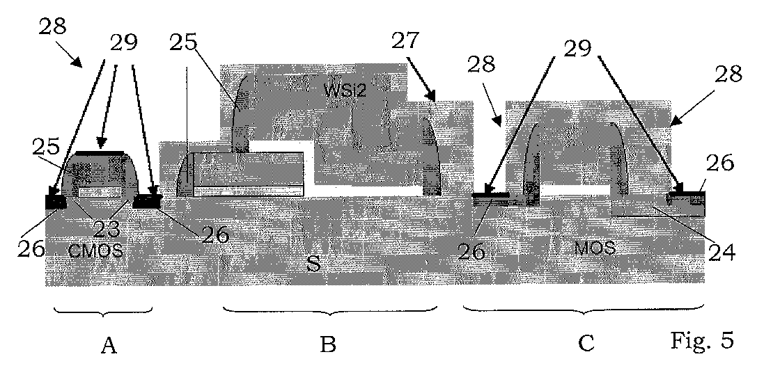
- Figures 2 to 5 are sectional views, drawn to an enlarged scale, of a portion of a semiconductor substrate during fabrication steps according to a first embodiment of the inventive process; and
- Figures 6 to 9 are enlarged sectional views, drawn to an enlarged scale, of a portion of a semiconductor substrate during fabrication steps according to a second embodiment of the inventive process.
- Referring to Figures 2 to 5, a first embodiment of the process for forming silicided CMOS transistors and MOS transistors on a common semiconductor substrate in accordance with this invention will now be described.
- The processing steps described here below are not exhaustive of a complete process for fabricating integrated circuits. This invention can be practiced along with integrated circuit fabrication techniques conventionally employed, and only conventional process steps, necessary for the understanding of the invention. will be described.
- Perspective views of portions of an integrated circuit during its fabrication are not drawn to scale, but rather to emphasize major features of the invention.
- In particular, a first
dielectric layer 14 and firstsemiconductor material layer 15 are provided on a semiconductor substrate S which includes a first portion A where CMOS devices are to be formed, a second portion B providing separation, and a third portion C where drain-extension MOS devices are to be formed. - The
first layer 16 is removed from the third portion C of thesubstrate 1 by a photolithographic operation followed by etching. - Advantageously, the first
dielectric layer 14 is an oxide layer from which the gate oxide layer of the CMOS transistors is formed, and thefirst layer 15 of semiconductor material is a polysilicon layer from which the layer POLY1 of the CMOS transistors is formed. - There is then a cascade formation, on the whole device, of a stack structure comprising a second
dielectric layer 16, e.g. silicon oxide, a secondsemiconductor material layer 17, e.g. polysilicon, and a low-resistivity layer 18, e.g. comprising tungsten. -
First openings 19 are provided in portion C, in both thesemiconductor material layer 17 andlow resistivity layer 18, to define agate region 20 of the RF application devices. - The second
semiconductor material layer 17 and low-resistivity layer 18 are removed from portion A completely. - Advantageously, the
dielectric layer 16 formed on thefirst polysilicon layer 15 is utilized as a screen during removal of the secondsemiconductor material layer 17 in the portion C of thesubstrate 14. - Thus, a
structure 21 is defined in portion B, which isolates the substrate portion A, where the CMOS devices are to be formed, from the substrate portion C where the RF application devices are to be formed. - Through a conventional photolithography technique followed by etching, openings 22' are made to define
gate regions 22 of the CMOS transistors in the portion A of thesubstrate 14, as shown in Figure 4. - The substrate is then implanted with first LDD (Lightly Doped Drain)
regions 23 to provide source and drain regions of the CMOS transistors. - Advantageously, drain
regions 24 of the drain-extension MOS transistors are also formed during this process step. - In particular, the
drain region 24 includes a lightly doped drift region adjacent to thegate region 20. - Conventional techniques are then applied to form
spacers 25 on the sidewalls of thegate regions 20 of the RF devices, and on those of thedivision structure 21 and thegate regions 22 of the CMOS transistors. - Thereafter, second heavily doped implanted
regions 26 are provided to complete the source and drain regions of the CMOS transistors, and the body and drain regions of the drain-extension MOS transistors. - A
protective layer 27 is deposited onto the whole device. Thisprotective layer 27 is removed from the substrate portion A completely to expose the substrate S. Theprotective layer 27 is provided withopenings 28 in the body and drain regions of the drain-extension MOS transistor. - The
protective layer 27 may be a dielectric layer. - A metal layer is formed on the whole device. This metal layer may be formed with a transition metal. The device is then subjected to a thermal process, so that the metal layer reacts with the substrate which is not covered by the
protective layer 27 and forms asilicide layer 29. - A second embodiment of the process according to the invention will now be described with reference to Figures 6 to 9.
- A
first dielectric layer 14a, firstsemiconductor material layer 15a, and seconddielectric layer 16a, e.g. silicon oxide, are provided on a semiconductor substrate S which includes a first portion A, second portion B, and third portion C. - The
second dielectric layer 16a is removed from the third portion C of thesubstrate 1 where the RF devices are to be formed, and from a portion of the second portion B adjacent to the third portion C, by a photolithographic operation followed by etching. - Advantageously, the first
dielectric layer 14a is an oxide layer with which the gate oxide layer of the CMOS transistors and the drain-extension MOS transistors is formed, and thefirst layer 15a of semiconductor material is a polysilicon layer by means of which the layer POLY1 of the CMOS transistors and a first portion of the gate region of the drain-extension MOS transistor are formed. - There is then a cascade formation, on the whole device, of a stack structure comprising a second
semiconductor material layer 17a, e.g. polysilicon, and a low-resistivity layer 18a, e.g. tungsten. -
First openings 19a are provided in the portion C, in the firstsemiconductor material layer 16a, in the secondsemiconductor material layer 17a, and in thelow resistivity layer 18a, to define agate region 20a for the RF application devices. - The second
semiconductor material layer 17a and the low-resistivity layer 18 are fully removed from the substrate portion A where the CMOS devices are to be formed. - Advantageously, the
second dielectric layer 16a formed on thefirst polysilicon layer 15a is utilized as a screen during removal of the first and secondsemiconductor material layers ports 19a. - Thus, a
structure 21a is defined in portion B to isolate the substrate portion A where the CMOS devices are to be formed from the substrate portion C where the RF application devices are to be formed. - Through a conventional photolithography technique followed by etching, gate regions 22a of the CMOS transistors are defined in the portion A of the
substrate 14a, as shown in Figure 4. - In the substrate first LDD implanted
regions 23a are then formed so as to provide source and drain regions for the CMOS transistors. - Advantageously, drift
regions 24a of the drain-extension MOS transistors are also formed during this process step. - Conventional techniques are then applied to form
spacers 25a on the sidewalls of thegate regions 20a of the RF devices, and on those of thedivision structure 21a and the gate regions 22a of the CMOS transistors. - Thereafter, second heavily doped implanted
regions 26a are provided to complete the source and drain regions of the CMOS transistors, and to complete the body and drain regions of the drain-extension MOS transistors. - A protective layer 27a is then deposited onto the whole device. This protective layer 27a is removed from the substrate portion A completely to expose the substrate S. The protective layer 27a is provided with
openings 28a at the body and drain regions of the drain-extension MOS transistor. - A metal layer is formed on the whole device. The device is then subjected to a thermal process so that the metal layer reacts with the uncovered substrate by the protective layer 27a and forms a
silicide layer 29a. - To summarize, the method of the invention allows high-density high-performance CMOS structures to be integrated on a common substrate along with high- performance drain-extension MOS structures, without introducing any dedicated process steps to make either structures.
- In particular, the
gate region 20 of the drain-extension MOS transistor is provided with a low-resistance layer 18 by depositing the low-resistance layer 18 onto thepolysilicon layer 17, while the heavily dopedregions 26 of the CMOS transistors and the drain-extension MOS transistors are silicided in a self-aligned silicidation process that will also silicide thegate regions 22 of the CMOS transistors.
Claims (9)
- A process for forming, on a common semiconductor substrate (S), CMOS transistors and drain-extension MOS transistors on at least first and second portions (A,C), respectively, of the substrate (S), the process comprising the following steps:the process being characterized in that it comprises the following steps:in said first portion (A), forming at least one CMOS transistor having a first gate region (22,22a) projecting from the substrate (S), and having respective source and drain regions formed in the substrate (S), each one including a first, lightly doped portion (23,23a) adjacent to the gate region (22,22a), and including a second, heavily doped portion (26,26a) within said first lightly doped portion (23,23a); andin said second portion (C), forming at least one drain-extension MOS transistor having a gate region (20,20a) projecting from the substrate (S), a source region including a first, heavily doped portion (26,26a) aligned to said gate region (20,20a), and a drain region formed in the substrate (S) and including a first, lightly doped portion (24,24a) adjacent to the gate region (20,20a), and a second, heavily doped portion (28,26a) within said first lightly doped portion (24,24a).forming a low-resistance layer (18,18a) on said gate region (20,20a) of the drain-extension MOS transistor;forming a protective layer (27,27a) on said gate region (20,20a) and said second lightly doped portion (24,24a) of the drain-extension MOS transistor;forming a metal layer over said second heavily doped portions (26,26a) of said CMOS transistor and said drain-extension MOS transistor, and on said gate region (22,22a) of said CMOS transistor; andoperating a thermal treatment so as make said metal layer react with the substrate (S) and the gate region (22) of said CMOS transistor, andform a silicide layer (29).
- A process according to Claim 1, characterized in that said CMOS transistor and said drain-extension MOS transistor are formed by the following steps:forming a first dielectric layer (14) on the whole substrate (S);forming a first semiconductor material layer (15) on said first dielectric layer (14) in said at least one first portion (A);forming, over the whole substrate (S), a stack structure comprising a second dielectric layer (16), second semiconductor layer (17), and low-resistance layer (18);defining first openings (19) in said second semiconductor layer (17) and said low-resistance layer (18) to provide said gate regions (20) of the drain-extension MOS transistors;completely removing said second semiconductor layer (17) and said low-resistance layer (19) from said first portion (A) of the substrate (S) by using said second dielectric layer (16) as a screen; anddefining second openings (22') in said second dielectric layer (16) and in said second semiconductor layer (15) to provide said gate regions (22) of the CMOS transistors.
- A process according to Claim 1, characterized in that said CMOS transistor and said drain-extension MOS transistor are formed by the following steps:forming, on the whole substrate (S), a stack structure comprising a first dielectric layer (14a), and a first semiconductor material layer (15a);forming a second dielectric layer (16a) in said at least one first portion (A);forming, on the whole substrate (S), a stack structure comprising a second semiconductor layer (17a) and a first low-resistance layer (18a);defining first openings (19a) in said first low-resistance layer (18a), said second semiconductor layer (17a), and said first semiconductor material layer (15a) to provide said gate regions (20a) of the vertical or lateral MOS transistors;completely removing said second semiconductor layer (17a) and said first low-resistance layer (18a) from said first portion (A) of the substrate (S) by using said second dielectric layer (16a) as a screen; anddefining second openings (22b) in said second dielectric layer (16a) and said second semiconductor layer (15a) to provide said gate regions (22a) of the CMOS transistors.
- A process according to Claim 1, characterized in that the step of forming said low-resistance layer (29a) is preceded by the following steps:implanting, in the substrate (S), said first lightly doped implanted regions (23,24) adjacent to said gate regions (20,22) of both the CMOS and the vertical or lateral MOS transistors;defining spacers (25) on the sidewalls of said gate regions (20,22); andimplanting, in the substrate (S), second heavily doped implanted regions (26) aligned to said spacers (25).
- A process according to either Claim 2 or 3, characterized in that said dielectric layers (14,16;14a,16a) are silicon oxide layers.
- A process according to either Claim 2 or 3, characterized in that said semiconductor layers (15,17;15a,17a) are polysilicon layers.
- A process according to Claim 1, characterized in that said first low-resistance layer (18;18a) comprises tungsten.
- A process according to Claim 1, characterized in that said metal layer comprises at least one transition metal.
- A process according to either Claim 2 or 3, characterized in that the substrate (S) has a second portion (B) extending between said first portion (A) and said second portion (C) where an division structure (21,21a) is provided between said first portion (A) and said second portion (C).
Priority Applications (2)
| Application Number | Priority Date | Filing Date | Title |
|---|---|---|---|
| EP02425807A EP1435648A1 (en) | 2002-12-30 | 2002-12-30 | Process of making CMOS and drain extension MOS transistors with silicided gate |
| US10/746,881 US7005336B2 (en) | 2002-12-30 | 2003-12-23 | Process for forming CMOS transistors and MOS transistors of the drain extension type, with a low gate region resistance, in the same semiconductor substrate |
Applications Claiming Priority (1)
| Application Number | Priority Date | Filing Date | Title |
|---|---|---|---|
| EP02425807A EP1435648A1 (en) | 2002-12-30 | 2002-12-30 | Process of making CMOS and drain extension MOS transistors with silicided gate |
Publications (1)
| Publication Number | Publication Date |
|---|---|
| EP1435648A1 true EP1435648A1 (en) | 2004-07-07 |
Family
ID=32479860
Family Applications (1)
| Application Number | Title | Priority Date | Filing Date |
|---|---|---|---|
| EP02425807A Withdrawn EP1435648A1 (en) | 2002-12-30 | 2002-12-30 | Process of making CMOS and drain extension MOS transistors with silicided gate |
Country Status (2)
| Country | Link |
|---|---|
| US (1) | US7005336B2 (en) |
| EP (1) | EP1435648A1 (en) |
Families Citing this family (5)
| Publication number | Priority date | Publication date | Assignee | Title |
|---|---|---|---|---|
| EP1915783A2 (en) * | 2005-08-10 | 2008-04-30 | Nxp B.V. | Ldmos transistor |
| JP4970185B2 (en) * | 2007-07-30 | 2012-07-04 | 株式会社東芝 | Semiconductor device and manufacturing method thereof |
| US10134641B2 (en) * | 2015-05-21 | 2018-11-20 | CoolStar Technology, Inc. | Enhanced integration of DMOS and CMOS semiconductor devices |
| US10950720B2 (en) * | 2017-10-23 | 2021-03-16 | Texas Instruments Incorporated | Electrostatic discharge guard ring with complementary drain extended devices |
| CN112331558B (en) * | 2020-10-23 | 2023-09-15 | 杭州芯迈半导体技术有限公司 | LDMOS transistor and manufacturing method |
Citations (6)
| Publication number | Priority date | Publication date | Assignee | Title |
|---|---|---|---|---|
| EP0928030A1 (en) * | 1997-12-31 | 1999-07-07 | STMicroelectronics S.r.l. | High voltage field-effect transistor and corresponding manufacturing method |
| EP0954029A1 (en) * | 1997-12-31 | 1999-11-03 | STMicroelectronics S.r.l. | An electronic structure comprising high and low voltage transistors, and a corresponding manufacturing method |
| EP0962982A1 (en) * | 1998-06-03 | 1999-12-08 | STMicroelectronics S.r.l. | Byte-switch structure for EEPROM memories |
| US6037222A (en) * | 1998-05-22 | 2000-03-14 | Taiwan Semiconductor Manufacturing Company | Method for fabricating a dual-gate dielectric module for memory embedded logic using salicide technology and polycide technology |
| US20020084492A1 (en) * | 2000-09-01 | 2002-07-04 | Jun Osanai | Complementary MOS semiconductor device and method of manufacturing the same |
| US20020098703A1 (en) * | 2001-01-19 | 2002-07-25 | Sun-Chieh Chien | Method for fabricating a MOS transistor of an embedded memory |
Family Cites Families (5)
| Publication number | Priority date | Publication date | Assignee | Title |
|---|---|---|---|---|
| US5030585A (en) * | 1990-03-22 | 1991-07-09 | Micron Technology, Inc. | Split-polysilicon CMOS DRAM process incorporating selective self-aligned silicidation of conductive regions and nitride blanket protection of N-channel regions during P-channel gate spacer formation |
| KR960001611B1 (en) * | 1991-03-06 | 1996-02-02 | 가부시끼가이샤 한도다이 에네르기 겐뀨쇼 | Insulated gate field effect semiconductor device and fabrication method thereof |
| US5665993A (en) * | 1994-09-29 | 1997-09-09 | Texas Instruments Incorporated | Integrated circuit including a FET device and Schottky diode |
| US6303479B1 (en) * | 1999-12-16 | 2001-10-16 | Spinnaker Semiconductor, Inc. | Method of manufacturing a short-channel FET with Schottky-barrier source and drain contacts |
| US6528850B1 (en) * | 2000-05-03 | 2003-03-04 | Linear Technology Corporation | High voltage MOS transistor with up-retro well |
-
2002
- 2002-12-30 EP EP02425807A patent/EP1435648A1/en not_active Withdrawn
-
2003
- 2003-12-23 US US10/746,881 patent/US7005336B2/en not_active Expired - Lifetime
Patent Citations (6)
| Publication number | Priority date | Publication date | Assignee | Title |
|---|---|---|---|---|
| EP0928030A1 (en) * | 1997-12-31 | 1999-07-07 | STMicroelectronics S.r.l. | High voltage field-effect transistor and corresponding manufacturing method |
| EP0954029A1 (en) * | 1997-12-31 | 1999-11-03 | STMicroelectronics S.r.l. | An electronic structure comprising high and low voltage transistors, and a corresponding manufacturing method |
| US6037222A (en) * | 1998-05-22 | 2000-03-14 | Taiwan Semiconductor Manufacturing Company | Method for fabricating a dual-gate dielectric module for memory embedded logic using salicide technology and polycide technology |
| EP0962982A1 (en) * | 1998-06-03 | 1999-12-08 | STMicroelectronics S.r.l. | Byte-switch structure for EEPROM memories |
| US20020084492A1 (en) * | 2000-09-01 | 2002-07-04 | Jun Osanai | Complementary MOS semiconductor device and method of manufacturing the same |
| US20020098703A1 (en) * | 2001-01-19 | 2002-07-25 | Sun-Chieh Chien | Method for fabricating a MOS transistor of an embedded memory |
Non-Patent Citations (1)
| Title |
|---|
| TSUI P G Y ET AL: "Integration of power LDMOS into a low-voltage 0.5 mu m BiCMOS technology", ELECTRON DEVICES MEETING, 1992. TECHNICAL DIGEST., INTERNATIONAL SAN FRANCISCO, CA, USA 13-16 DEC. 1992, NEW YORK, NY, USA,IEEE, US, 13 December 1992 (1992-12-13), pages 27 - 30, XP010106441, ISBN: 0-7803-0817-4 * |
Also Published As
| Publication number | Publication date |
|---|---|
| US20040229438A1 (en) | 2004-11-18 |
| US7005336B2 (en) | 2006-02-28 |
Similar Documents
| Publication | Publication Date | Title |
|---|---|---|
| US6630720B1 (en) | Asymmetric semiconductor device having dual work function gate and method of fabrication | |
| US6864135B2 (en) | Semiconductor fabrication process using transistor spacers of differing widths | |
| KR101113009B1 (en) | Method and apparatus for forming an ??? body-contacted transistor | |
| US6107160A (en) | MOSFET having buried shield plate for reduced gate/drain capacitance | |
| JP4971593B2 (en) | Manufacturing method of semiconductor device | |
| EP1103074A2 (en) | Mosfet having self-aligned gate and buried shield and method of making same | |
| US8748277B2 (en) | Method for fabricating a MOS transistor with reduced channel length variation | |
| EP0954029A1 (en) | An electronic structure comprising high and low voltage transistors, and a corresponding manufacturing method | |
| US7005336B2 (en) | Process for forming CMOS transistors and MOS transistors of the drain extension type, with a low gate region resistance, in the same semiconductor substrate | |
| US6762468B2 (en) | Semiconductor device and method of manufacturing the same | |
| US8076703B2 (en) | Semiconductor device and methods for fabricating same | |
| JPH10261789A (en) | Electrode structure for semiconductor device | |
| JP2005228906A (en) | Semiconductor device and manufacturing method thereof | |
| US7364959B2 (en) | Method for manufacturing a MOS transistor | |
| JP3926964B2 (en) | Semiconductor device and manufacturing method thereof | |
| US7638837B2 (en) | Stress enhanced semiconductor device and methods for fabricating same | |
| JP4965072B2 (en) | Manufacturing method of SOI semiconductor device | |
| JPH11238817A (en) | Semiconductor device and its manufacture | |
| US6949803B2 (en) | Manufacturing process for a high voltage transistor integrated on a semiconductor substrate with non-volatile memory cells and corresponding transistor | |
| JPH08250726A (en) | Insulated gate type field effect transistor and manufacturing method thereof | |
| JPH06204255A (en) | Manufacture of semiconductor device | |
| JPH0786423A (en) | Manufacture of mis type semiconductor integrated circuit device | |
| JP2007067438A (en) | Semiconductor device and manufacturing method thereof | |
| JPH02138747A (en) | Semiconductor device and its manufacturing method |
Legal Events
| Date | Code | Title | Description |
|---|---|---|---|
| PUAI | Public reference made under article 153(3) epc to a published international application that has entered the european phase |
Free format text: ORIGINAL CODE: 0009012 |
|
| AK | Designated contracting states |
Kind code of ref document: A1 Designated state(s): AT BE BG CH CY CZ DE DK EE ES FI FR GB GR IE IT LI LU MC NL PT SE SI SK TR |
|
| AX | Request for extension of the european patent |
Extension state: AL LT LV MK RO |
|
| 17P | Request for examination filed |
Effective date: 20050103 |
|
| AKX | Designation fees paid |
Designated state(s): DE FR GB IT |
|
| 17Q | First examination report despatched |
Effective date: 20050613 |
|
| 17Q | First examination report despatched |
Effective date: 20050613 |
|
| 17Q | First examination report despatched |
Effective date: 20050613 |
|
| STAA | Information on the status of an ep patent application or granted ep patent |
Free format text: STATUS: THE APPLICATION IS DEEMED TO BE WITHDRAWN |
|
| 18D | Application deemed to be withdrawn |
Effective date: 20080603 |